SkatterBencher #86: Intel Graphics (Arrow Lake) Overclocked to 3100 MHz

We overclock and undervolt the Intel Graphics (Arrow Lake) to 3100 MHz with the ASUS ROG Maximus Z890 Apex motherboard and custom loop liquid cooling.
We do this by exploring several of the Arrow Lake overclocking tools which I previously covered on this channel.
In this guide, I break down the Intel Graphics tuning process into five unique overclocking strategies for beginners and advanced overclockers.
- First, we enabled 200S Boost and ASUS MCE,
- Second, we overclock the integrated graphics without voltage adjustments,
- Third, we tune the memory subsystem performance,
- Fourth, we push the integrated graphics with voltage adjustments,
- And, finally, we use BCLK overclocking to maximize performance.
However, before we jump into overclocking, let us quickly review the hardware and benchmarks used in this guide.
Intel Graphics (Arrow Lake): Introduction
Intel Graphics is the official product name of the Arrow Lake IGP. It is the successor to the Intel UHD Graphics 770 integrated in the Core i9-14900K and Core i9-13900K. We overclocked that IGP in SkatterBencher #57 up to 2500 MHz.
The Arrow Lake integrated graphics features 4 Xe-LPG cores. This is an improved version of the Xe-LP cores from Raptor Lake as we get double the Execution Units. However, it still only features the Alchemist architecture as opposed to Lunar Lake’s Battlemage.
The 4 Xe-cores consist of 64 execution units and 512 shader units. The maximum boost frequency is 2000 MHz, which is 350 MHz higher than the boost frequency of the UHD 770.
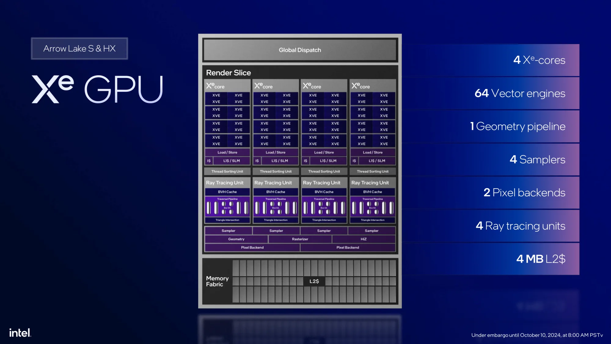
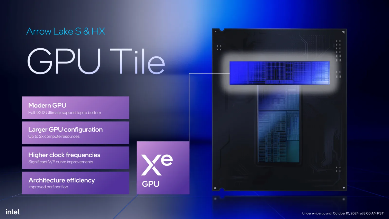
Another big change with Arrow Lake is its tile-based architecture. The Arrow Lake integrated graphics cores are located on the Graphics Tile and thus disconnected from the other Compute IP blocks, including the last-level cache. Furthermore, the graphics tile only includes the GPU cores, not any of the other media and display IP blocks.
Platform Overview
The system we’re overclocking today consists of the following hardware.
| Item | SKU | Price (USD) |
|---|---|---|
| CPU | Intel Core Ultra 9 285K | 640 |
| Motherboard | ASUS ROG Maximus Z890 Apex | 714 |
| CPU Cooling | EK-Quantum Velocity2 EK-Quantum Kinetic FLT 240 D5 EK-Quantum Surface P480M – Black EK-Furious Meltemi 120 (x4) | 150 240 150 |
| Memory | Corsair Vengeance RGB 48GB DDR5-8000 CUDIMM | 300 |
| Power Supply | Enermax Revolution ATX 3.0 1200W | 200 |
| Storage | AGI 512GB NVMe M.2 Gen3 | 75 |
| Chassis | Open Benchtable V2 | 200 |
| Telemetry | BENCHLAB | 200 |
Benchmark Software
We use Windows 11 and the following benchmark applications to measure performance and ensure system stability.
Intel Graphics (Arrow Lake): Stock Performance
Before starting overclocking, we must check the system performance at default settings.
In the past, there was some confusion about what constitutes default settings for Intel processors. For Arrow Lake, Intel spent extra resources clarifying to industry and media partners what constitutes default settings.
Intel Arrow Lake Default Settings
Intel defines three power profiles for the Arrow Lake processors: baseline, performance, and extreme.
- The Baseline profile is provided for systems or motherboards with inadequate power delivery requirements to meet the performance profile. You can typically find it referenced as “Intel Default Baseline Profile.”
- The Performance profile is recommended by Intel as the default profile for most systems. In particular, high-end motherboards or gaming systems. You can typically find it referenced as “Intel Default Performance Profile.”
- The Extreme profile is provided as guidance to system designers or motherboards that intend to support overclocking. This profile is not validated by Intel and, when used, may void warranty terms.

The default settings must be in place on the first boot, after a BIOS update, or when a new CPU is installed. When users change the default settings, there should be a BIOS warning informing the users that the settings deviate from the Intel default settings.
For the purpose of this guide, we follow Intel’s direction and rely on the Performance profile for the default settings.
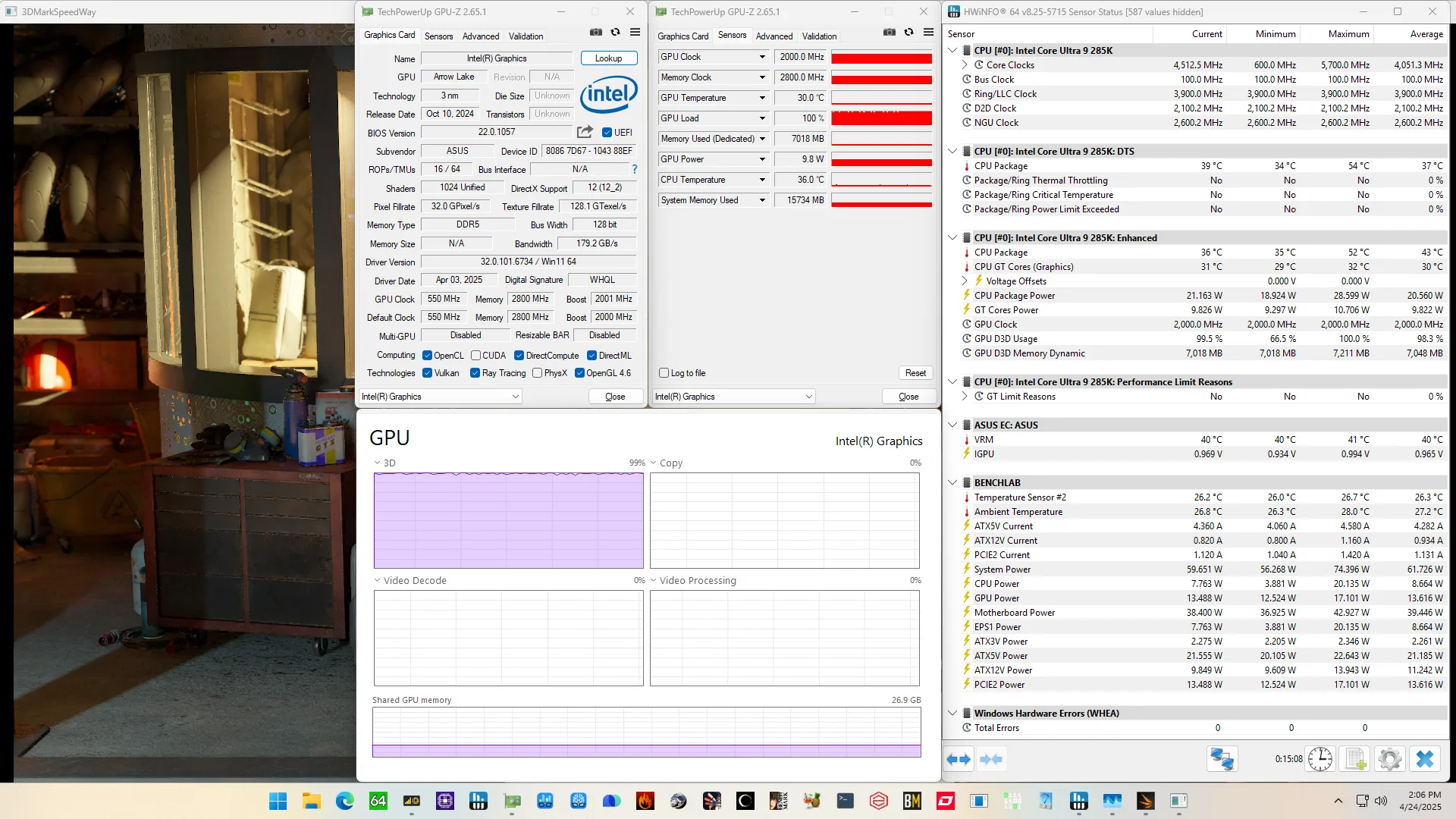
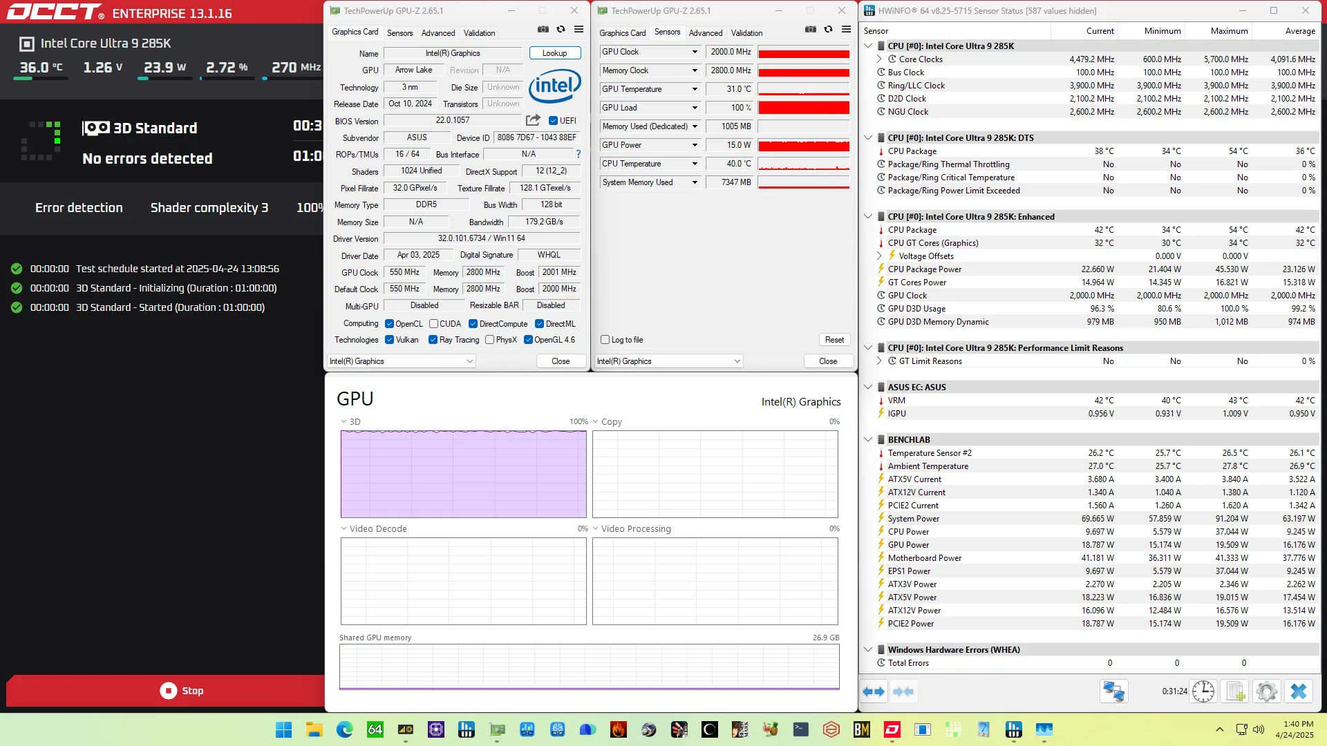
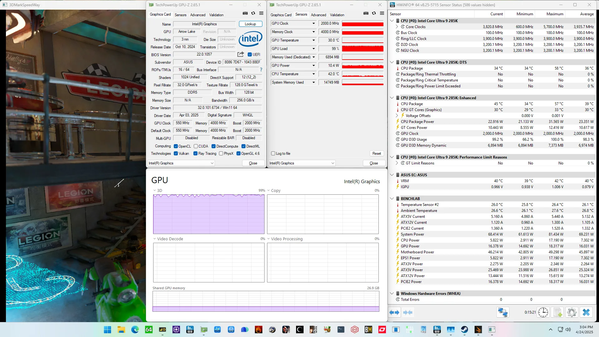
Here is the benchmark performance at stock
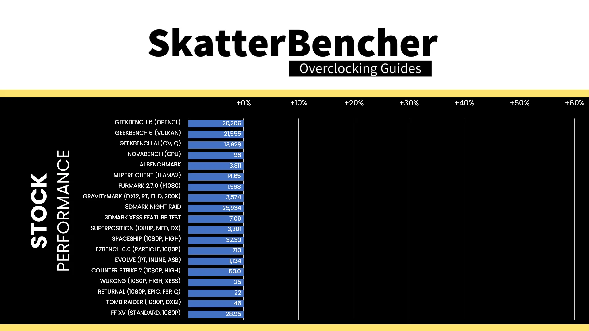
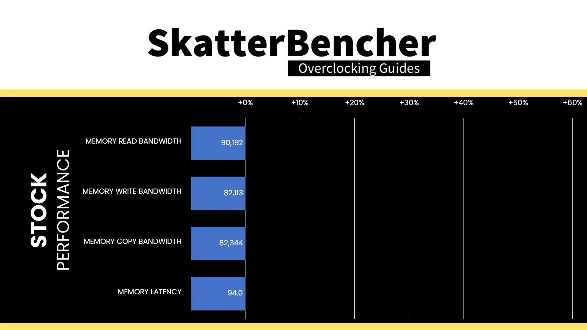
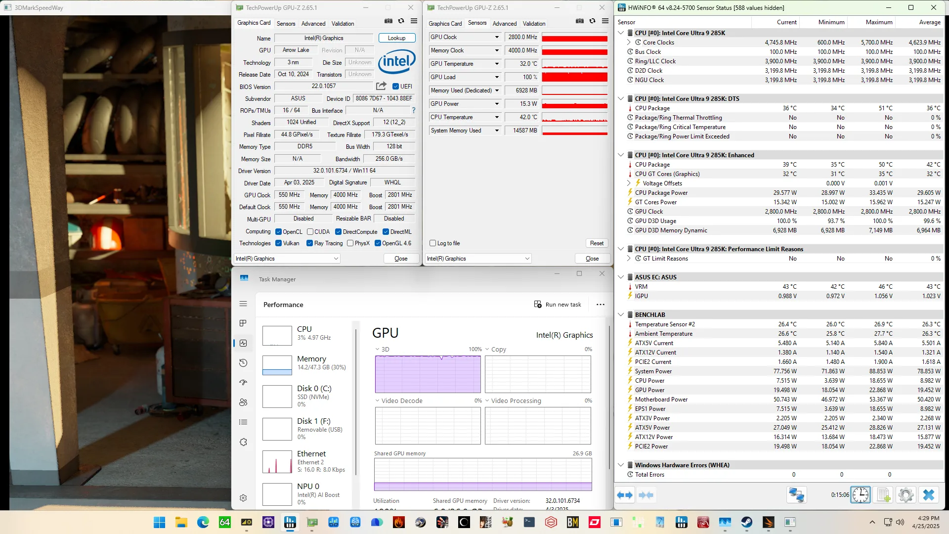
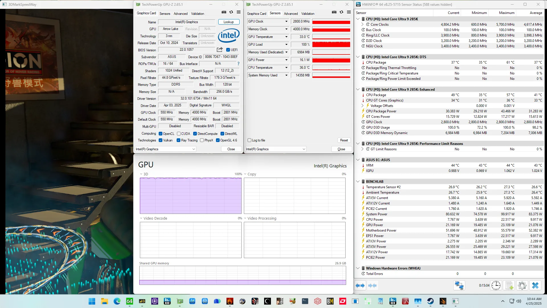
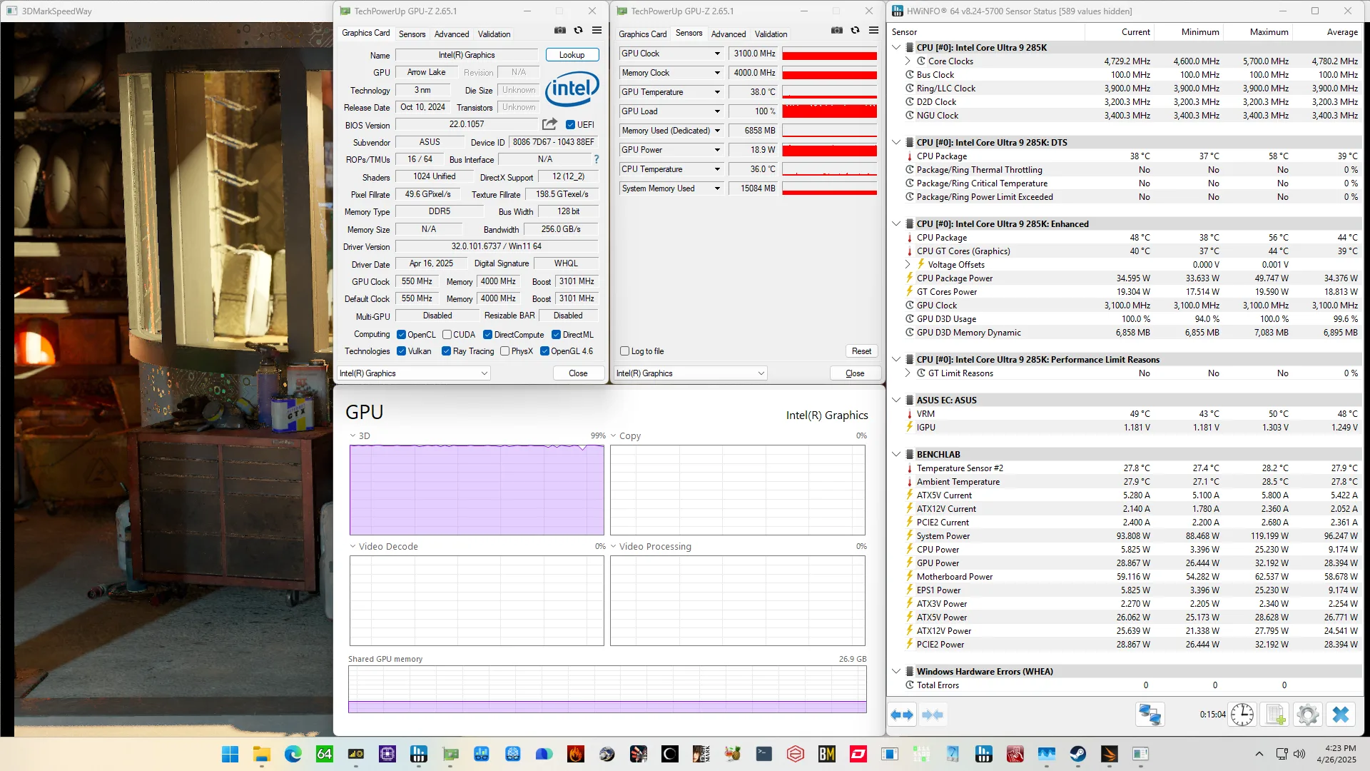
When running the 3DMark Speed Way Stability Test, the average GPU clock is 2000 MHz with 0.965 volts. The GPU memory clock is 2800 MHz. The average GPU Temperature is 30 degrees Celsius, and the average GPU Cores Power is 9.8 watts.
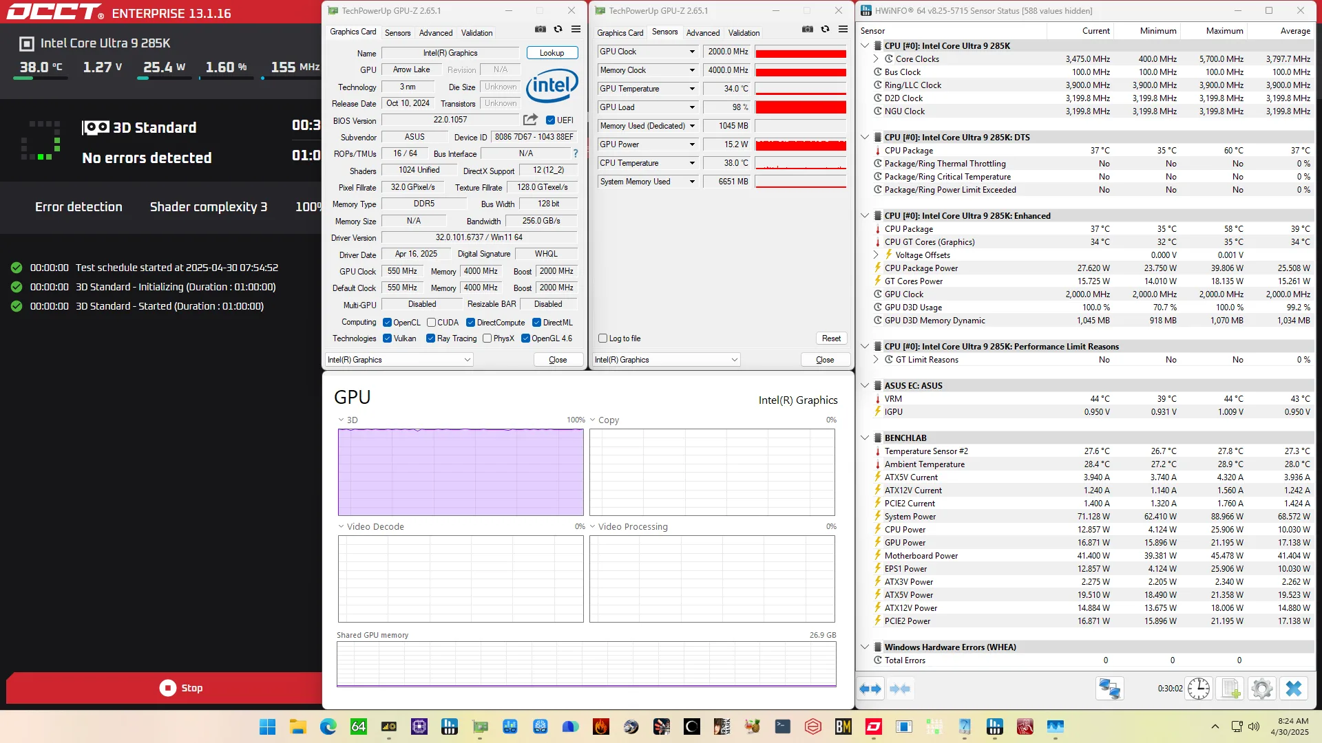
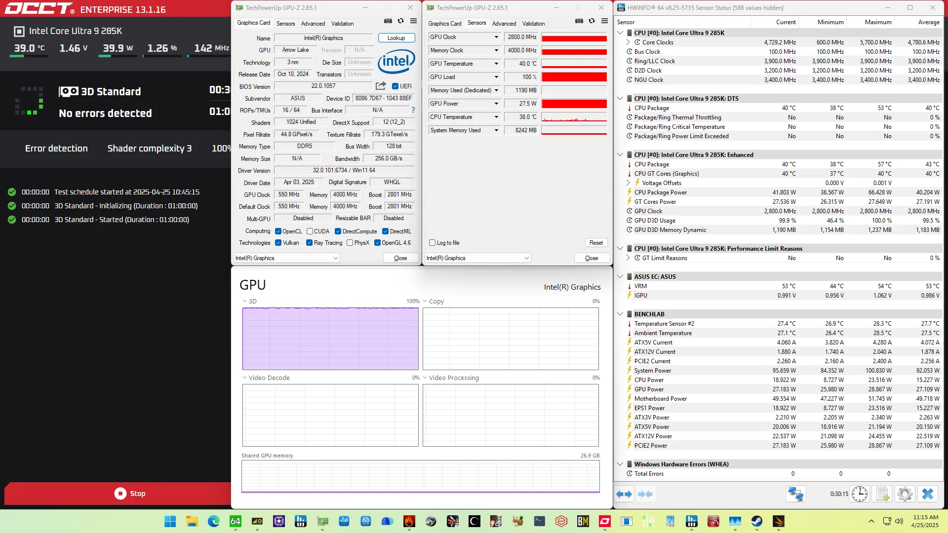
When running the OCCT 3D Standard Stress Test, the average GPU clock is 2000 MHz with 0.950 volts. The GPU memory clock is 2800 MHz. The average GPU Temperature is 32 degrees Celsius, and the average GPU Cores Power is 15.3 watts.
Of course, we can increase the maximum power consumption limit using Intel Turbo Boost Power Limits. That’s what we’ll do in our first overclocking strategy.
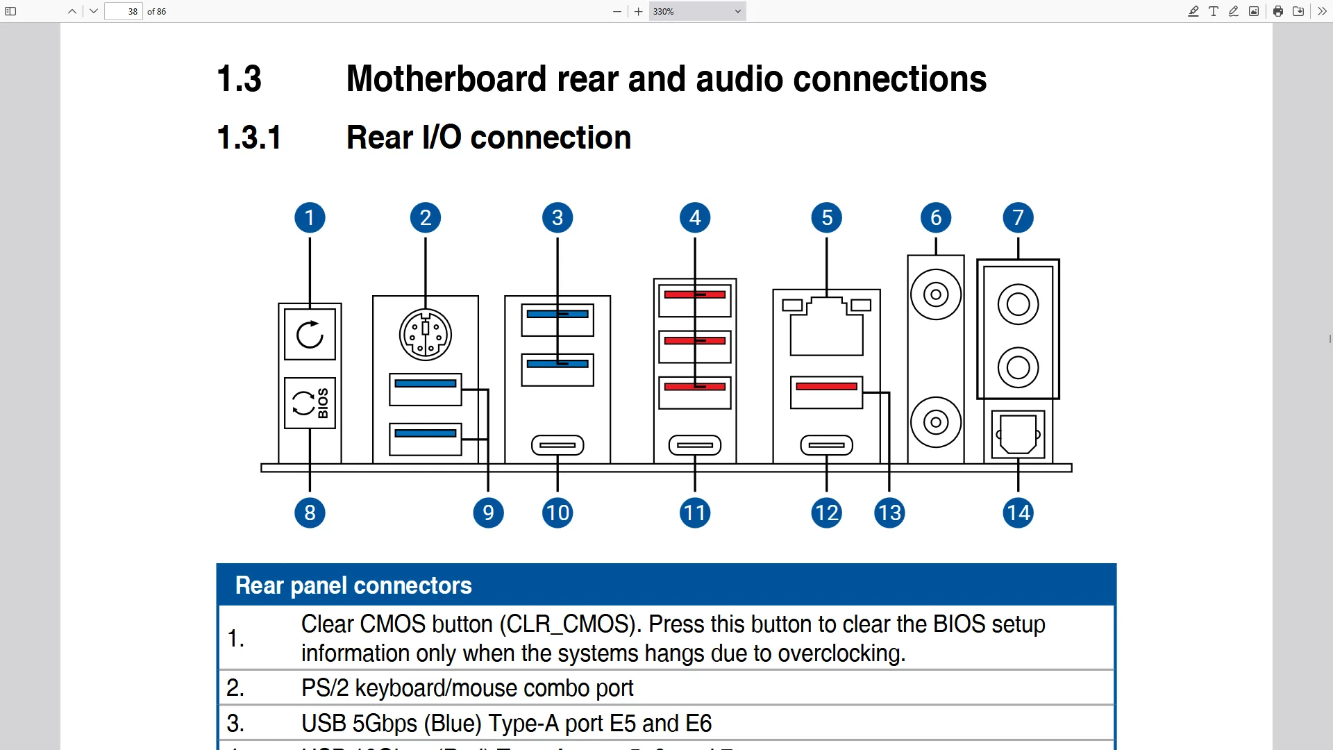
However, before we get going, make sure to locate the CMOS Clear button. Pressing the Clear CMOS button will reset all your BIOS settings to default, which is helpful if you want to start your BIOS configuration from scratch. The Clear CMOS button is located on the back I/O of the motherboard.
OC Strategy #1: 200S Boost + MCE
In our first overclocking strategy, we simply take advantage of enabling Intel 200S Boost and optimizing Intel Turbo Boost 2.0 power limits.
Intel 200S Boost
Intel 200S Boost is an Intel overclocking technology that enables NGU, D2D, and memory overclocking on Arrow Lake K-SKU processors without voiding warranty.
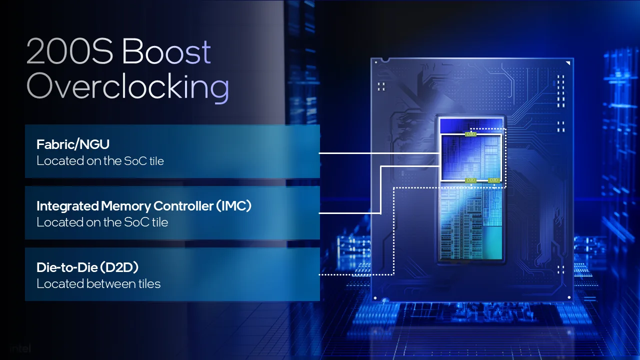
The 200S Boost program specifically enables for the creation of a motherboard BIOS option or profile that loads an OEM/ODM-tested set of “up to” values geared towards increasing performance on their platform. The “up to” values include restrictions on the voltage and frequency for the DRAM, D2D, and NGU.
Practically, 200S Boost is an easy way to enable XMP 3.0 without voiding the warranty because, yes, enabling XMP still technically voids warranty.
Intel Turbo Boost 2.0 Power Limits
Intel Turbo Boost 2.0 Technology allows the processor cores to run faster than the base operating frequency if the processor is operating below rated power, temperature, and current specification limits. The ultimate advantage is opportunistic performance improvements in both multi-threaded and single-threaded workloads.
The turbo boost algorithm works according to an EWMA formula. This stands for Exponentially Weighted Moving Average. There are three main parameters to consider: PL1, PL2, and Tau.

- Power Limit 1, or PL1, is the threshold that the average power will not exceed. Historically, this has always been set equal to Intel’s advertised TDP. Very importantly, PL1 should not be set higher than the thermal solution cooling limits.
- Power Limit 2, or PL2, is the maximum power the processor is allowed to use for a limited amount of time.
- Tau is a weighing constant used in the algorithm to calculate the moving average power consumption. Tau, in seconds, is the time window for calculating the average power consumption. If the average power consumed is higher than PL1 the CPU will reduce the CPU frequency.
Turbo Boost 2.0 Technology has evolved over the past years to incorporate a lot of power, thermal, and electrical performance limiters, including PL3, PL4, IccMax, TCC_Offset, VR_TDC, RATL, Pmax, and many more. It includes package-wide as well as IP-specific power management parameters. So, the integrated graphics has specific limits constraining its performance.
The only relevant Turbo Boost 2.0 performance limiters for Intel Graphics on Arrow Lake desktop CPUs is the ICCMax and the maximum voltage. The ICCMax is set to 40A by default and the voltage limit to approximately 1.05V. We’ll cover this in the upcoming overclocking strategies.
An easy ASUS MultiCore Enhancement option on ASUS motherboards allows you to unleash the Turbo Boost power limits. Set the option to Enabled – Remove All Limits and enjoy maximum performance.
BIOS Settings & Benchmark Results
Upon entering the BIOS
- Go to the Extreme Tweaker menu
- Set Performance Preferences to Intel Default
- Set Intel Default Settings to Performance
- Set Intel 200S Boost to Enabled
- Set ASUS MultiCore Enhancement to Enabled – Remove All Limits
Then save and exit the BIOS.
We re-ran the benchmarks and checked the performance increase compared to the default operation.


As expected, increasing the performance of the memory subsystem through overclocking of the system memory and NGU has a positive impact on the IGP performance. This is not dissimilar to other integrated graphics we’ve overclocked on this channel. The Geomean performance improvement is +6.37%, and we get a maximum improvement of +14.99% in Furmark.
When running the 3DMark Speed Way Stability Test, the average GPU clock is 2000 MHz with 0.979 volts. The GPU memory clock is 4000 MHz. The average GPU Temperature is 30 degrees Celsius, and the average GPU Cores Power is 10.6 watts.
When running the OCCT 3D Standard Stress Test, the average GPU clock is 2000 MHz with 0.950 volts. The GPU memory clock is 4000 MHz. The average GPU Temperature is 34 degrees Celsius, and the average GPU Cores Power is 15.3 watts.
OC Strategy #2: GPU Overclock
In our second overclocking strategy, we overclock the Intel Graphics without adjusting the operating voltage. For this, we must abandon the Intel 200S Boost program and configure the settings manually with ASUS Advanced OC Profile and XMP 3.0.
ASUS Advanced OC Profile
As I mentioned earlier, Intel has clarified the rules of engagement by defining what constitutes default settings. In doing so, it created stricter rules for default BIOS settings but also opened up new avenues for innovation. One such innovation is the ASUS Advanced OC Profile.
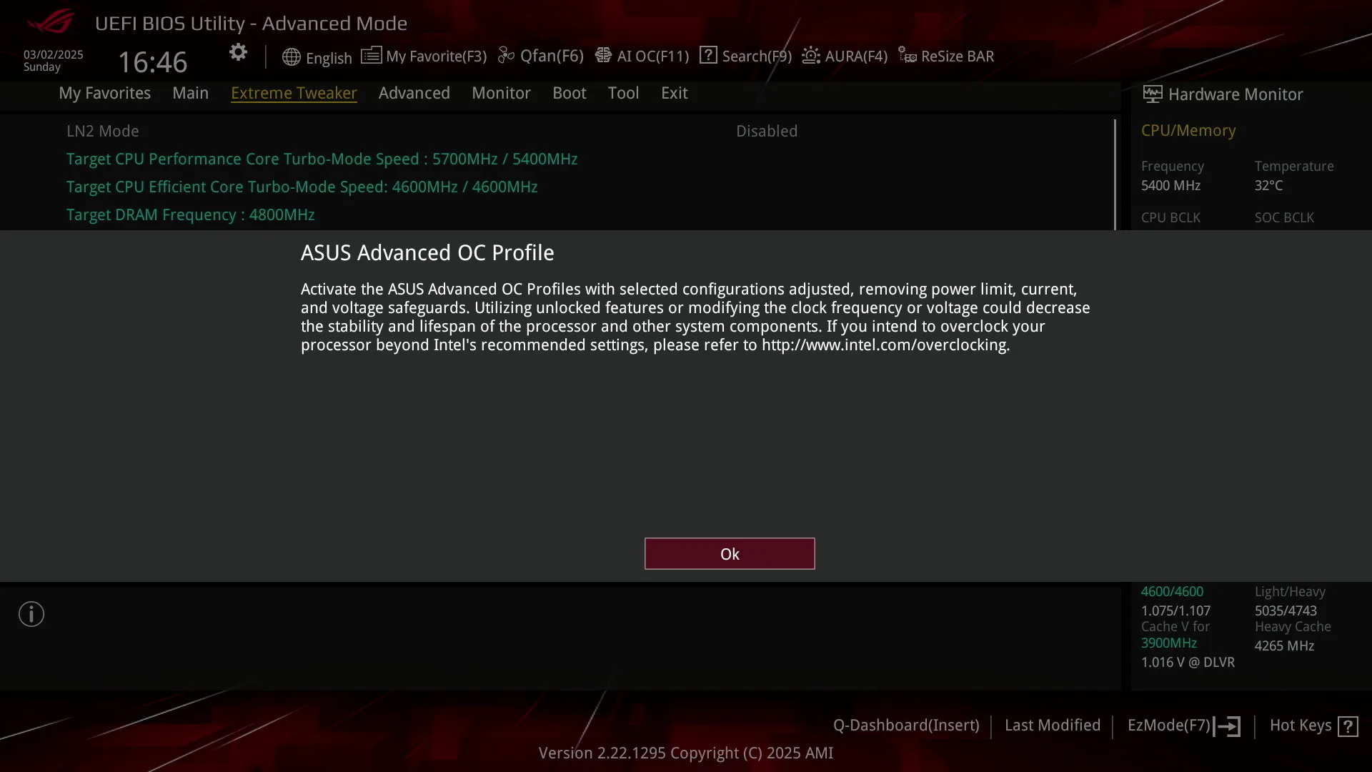
In essence, the ASUS Advanced OC Profile sets up the BIOS so it’s ready for overclocking. Not only does it reconfigure some of the parameters included in the definition of Intel’s Default Profiles, but it also configures a number of other settings related to power-saving and performance limiters.
By modifying those parameters, it’s possible to improve the system performance. Most importantly for our guide, however, is that you’re required to switch to the Advanced OC Profile for any kind of overclocking.
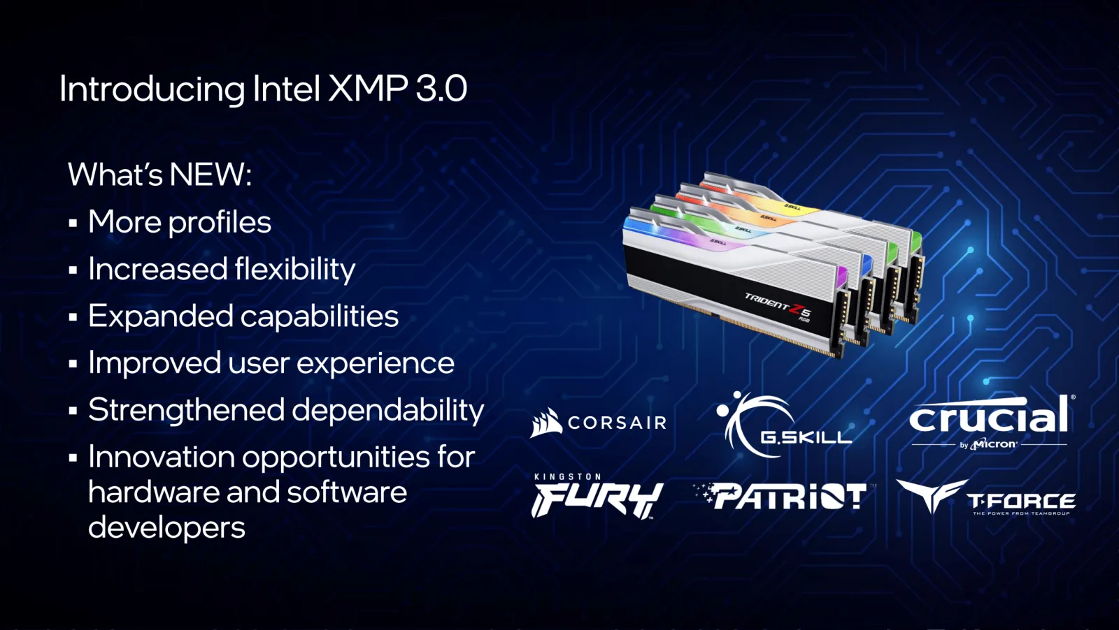
Intel Extreme Memory Profile 3.0
Intel Extreme Memory Profile 3.0 is the new XMP standard for DDR5 memory and is the successor to XMP 2.0 for DDR4 memory. It was introduced together with the Alder Lake processors in 2021. It is largely based on the XMP 2.0 standard but has additional functionality.
The XMP 3.0 standard is designed with six sections. One global section describes the generic data that is used across all profiles. The other five sections are designed for five profiles, respectively.
- Profile 1 is meant for the performance profile (this is the standard XMP as we know it)
- Profile 2 is designed for the extreme settings (this could be a higher frequency at higher voltage)
- Profile 3 is designed for the fastest settings (this could be tighter timings at higher voltage)
- Profiles 4 and 5 are rewritable and meant for user custom settings
Each profile has a wide range of configurable fields related to voltage, frequency, and memory timings, including:
- Voltage: Module VPP, VDD, VDDQ, Memory Controller Voltage
- Primary Timings: tCL, tRCD, tRP, tRAS, Command Rate
- Secondary Timings: tRC, tWR, tRFC1, tRFC2, tRFCsb
- Miscellaneous: Dynamic Memory Boost support, Real-Time Memory Frequency OC support, Vendor ID
XMP allows memory vendors such as Corsair to program higher performance settings onto the memory sticks. If the motherboard supports XMP, you can enable higher performance with a single BIOS setting. So, it saves you lots of manual configuration.
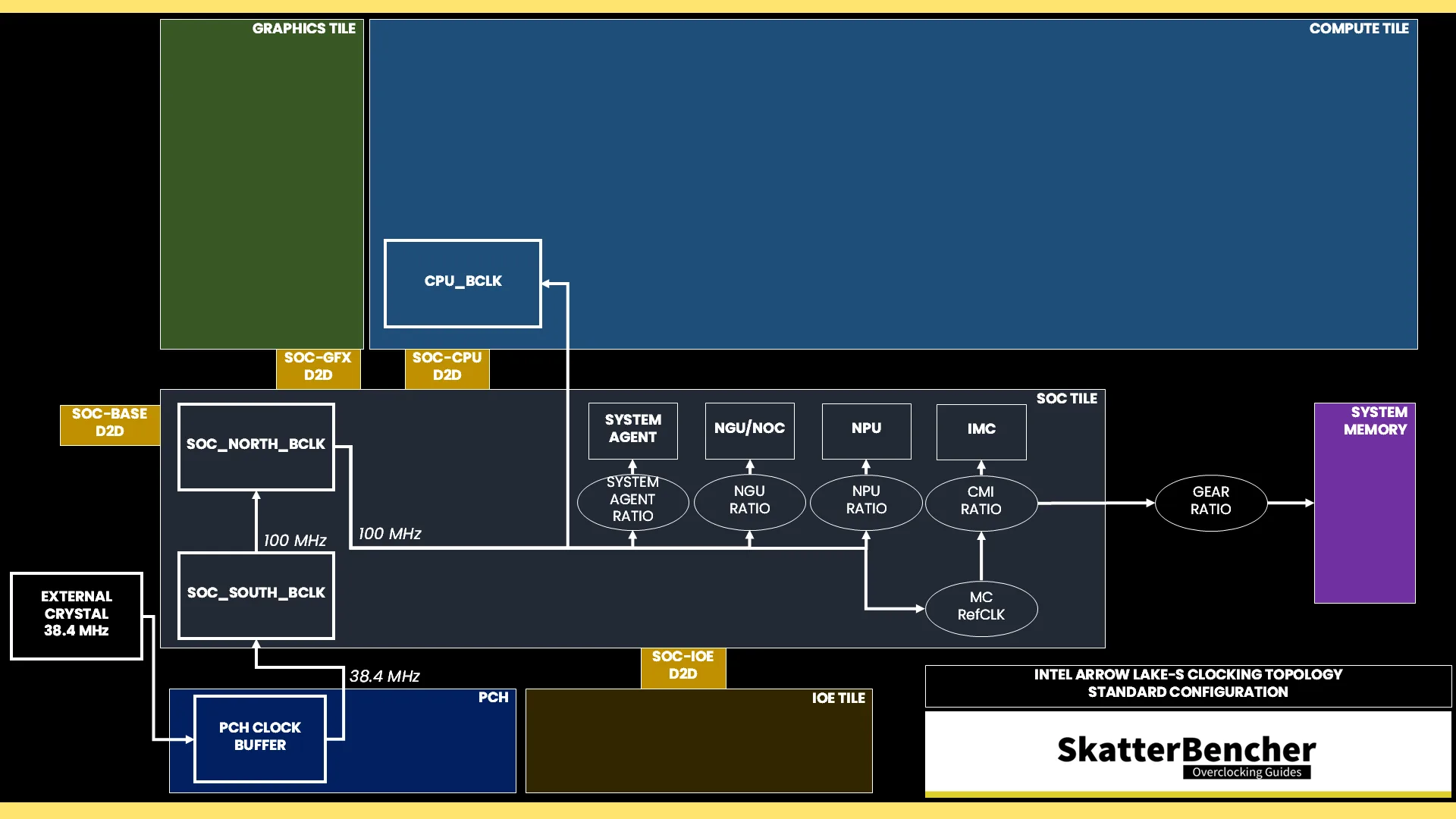
Intel Graphics (Arrow Lake) Clocking Topology
The clocking of the Arrow Lake integrated graphics is similar to previous architectures: a reference clock is multiplied with a graphics ratio to achieve the eventual operating frequency.
Reference Clock
The 100 MHz reference clock is generated internally by the SoC PLL. However, it can also be clocked with an external clock generator. I’ll cover this in more detail in the final overclocking strategy. The 100 MHz reference clock is divided by two (2) to achieve a 50 MHz base clock frequency for the integrated graphics. This can be a little confusing because the graphics ratio in the BIOS may not match the ratio displayed in XTU.
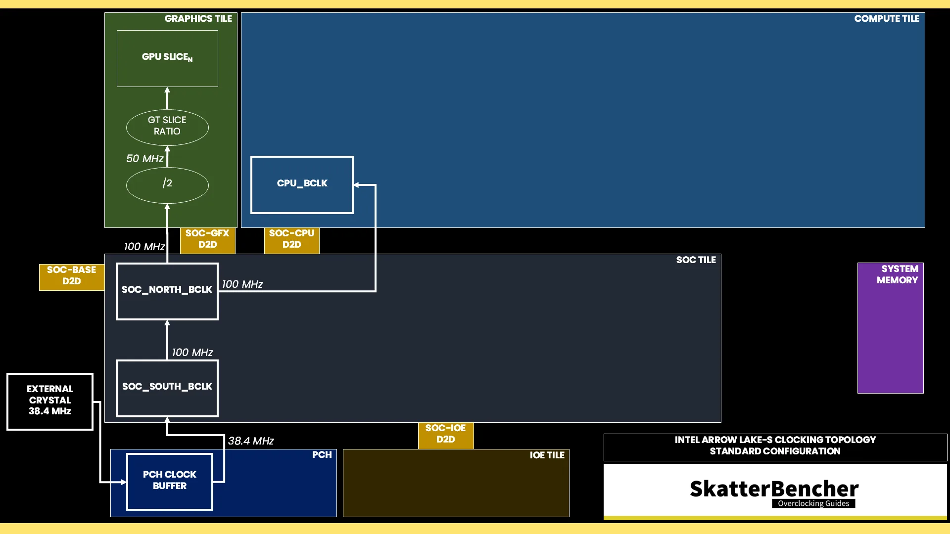
GT Ratio
The reference clock is multiplied by the GT ratio to achieve the final clock frequency. The GT Ratio is determined by the graphics voltage-frequency curve which I’ll cover next. Effectively, the GT ratio configured in the BIOS acts as a frequency ceiling or target frequency as it’s still subject to a variety of performance limiters.
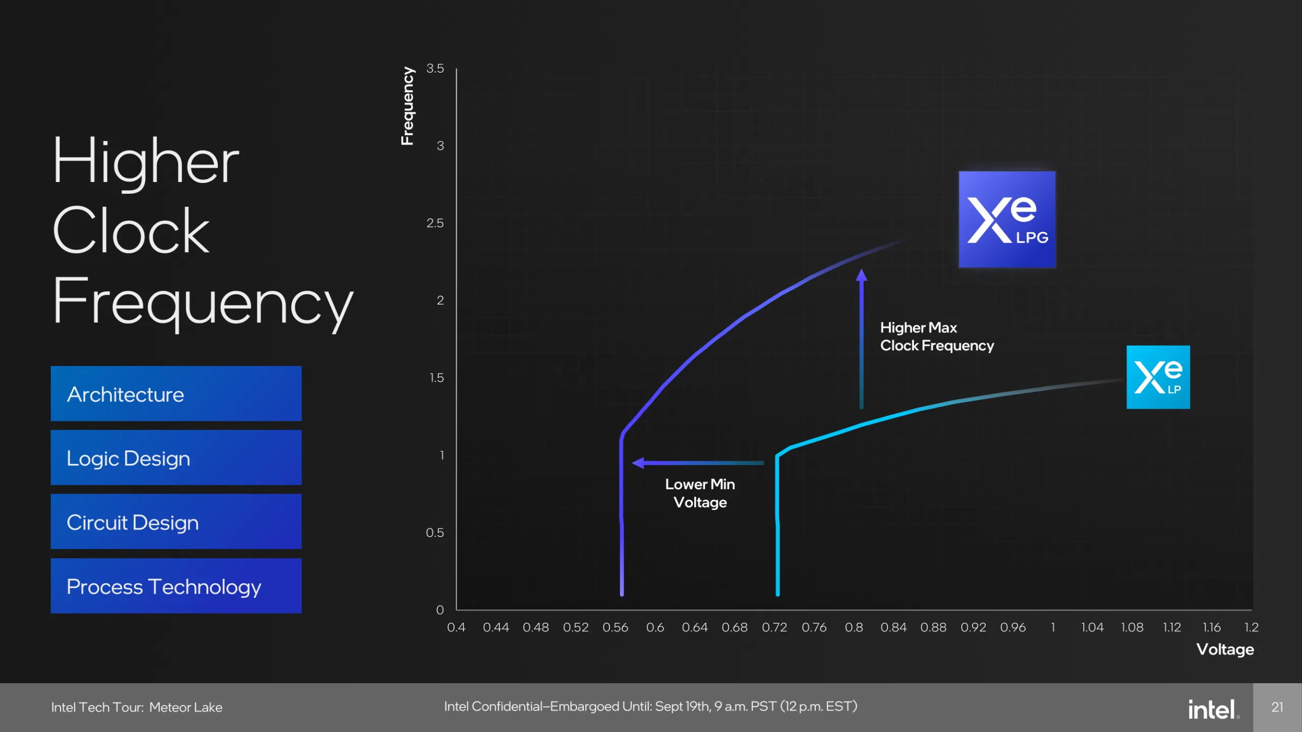
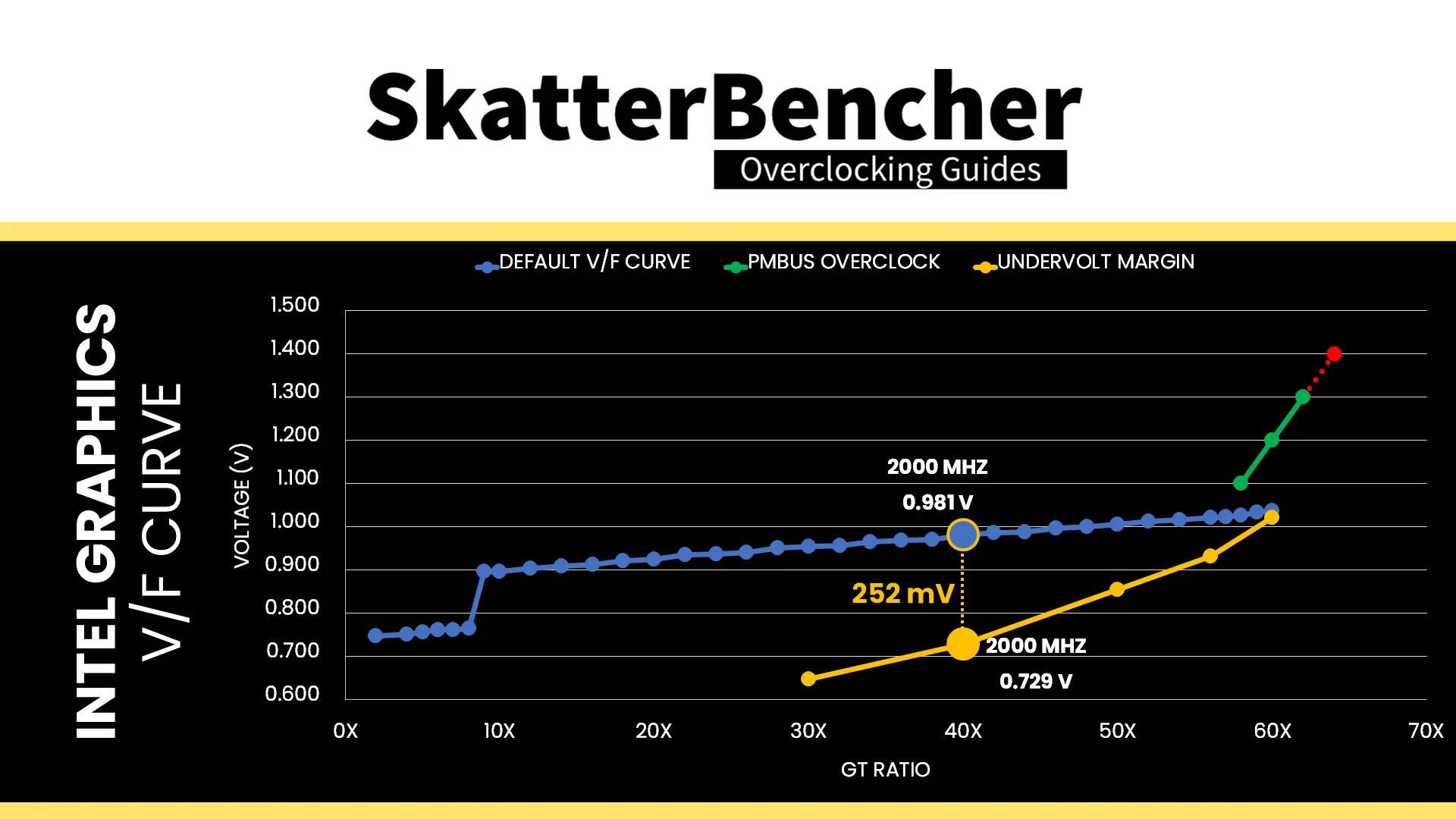
V/F Curve
The V/F curve for the Intel Graphics for Arrow Lake doesn’t quite follow the same rules as it did for previous generations’ integrated graphics. Rather than having a defined maximum turbo frequency with an associated maximum voltage, it seems the V/F curve is defined for many points beyond the default maximum boost frequency. Therefore, it resembles Arc discrete graphics cards more.
Here’s the manually traced V/F curve for this particular integrated graphics. The voltage starts at 748 mV for 100 MHz, and gradually goes up to 765mV at 400 MHz. Then, it takes a big jump to 897mV for 450 MHz. Finally, it increases nearly linearly to 1.04V for 3000 MHz.
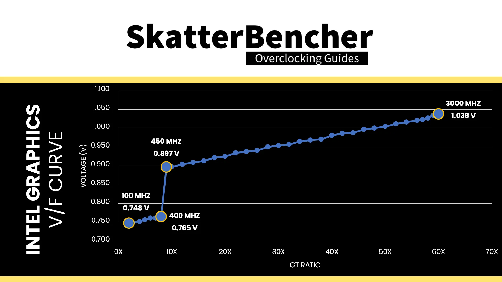
It’s possible the V/F curve extends beyond 3 GHz. However, unfortunately, we run into the voltage limiter causing the frequency to throttle in a similar way we saw with the discrete Arc graphics cards. I’ll discuss this in greater detail in OC Strategy #4 when we start playing around with voltage configuration.
Intel Graphics (Arrow Lake) Overclocking Process
The overclocking process for Intel Graphics is pretty straight-forward: we can use XTU to adjust the GT ratio in the operating system and check for stability.
Two notes to the overclocking process:
First, the graphics ratio in XTU is different from the BIOS. That’s perhaps because the XTU team wanted to make it more user-friendly to beginner overclockers since not everyone’s aware that the graphics base clock is 50 MHz rather than 100 MHz. So, when you know the maximum frequency in XTU just multiple the ratio by two for BIOS configuration.
Second, for me, the limiting workload was not the traditional heavy workloads like Furmark or OCCT, or even a modern 3DMark like Speed Way. Instead, 3DMark Night Raid was the most sensitive to overclocking and was the first to show signs of instability with higher frequencies (even though Night Raid uses a lot less power than a Furmark or OCCT). This is another good reminder that you always need to use a variety of workloads when checking for stability while overclocking.
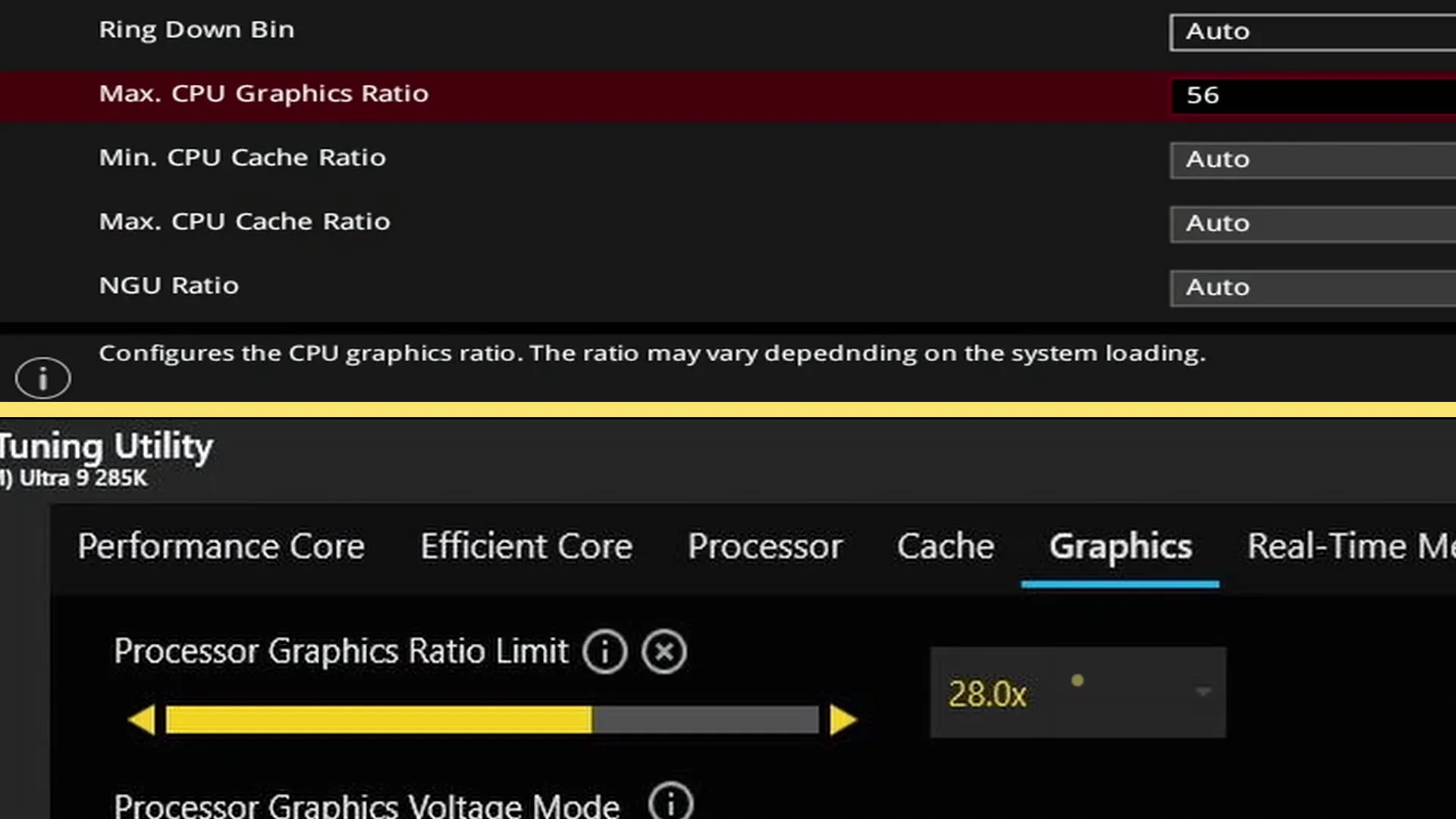
BIOS Settings & Benchmark Results
Upon entering the BIOS
- Go to the Extreme Tweaker menu
- Set Performance Preferences to ASUS Advanced OC Profile
- Set Ai Overclock Tuner to XMP I
- Set ASUS MultiCore Enhancement to Enabled – Remove All Limits
- Set Max. CPU Graphics Ratio to 56
- Set NGU Ratio to 32
- Set CPU System Agent Voltage to Manual Mode
- Set CPU System Agent Voltage Override to 1.200
Then save and exit the BIOS.
We re-ran the benchmarks and checked the performance increase compared to the default operation.
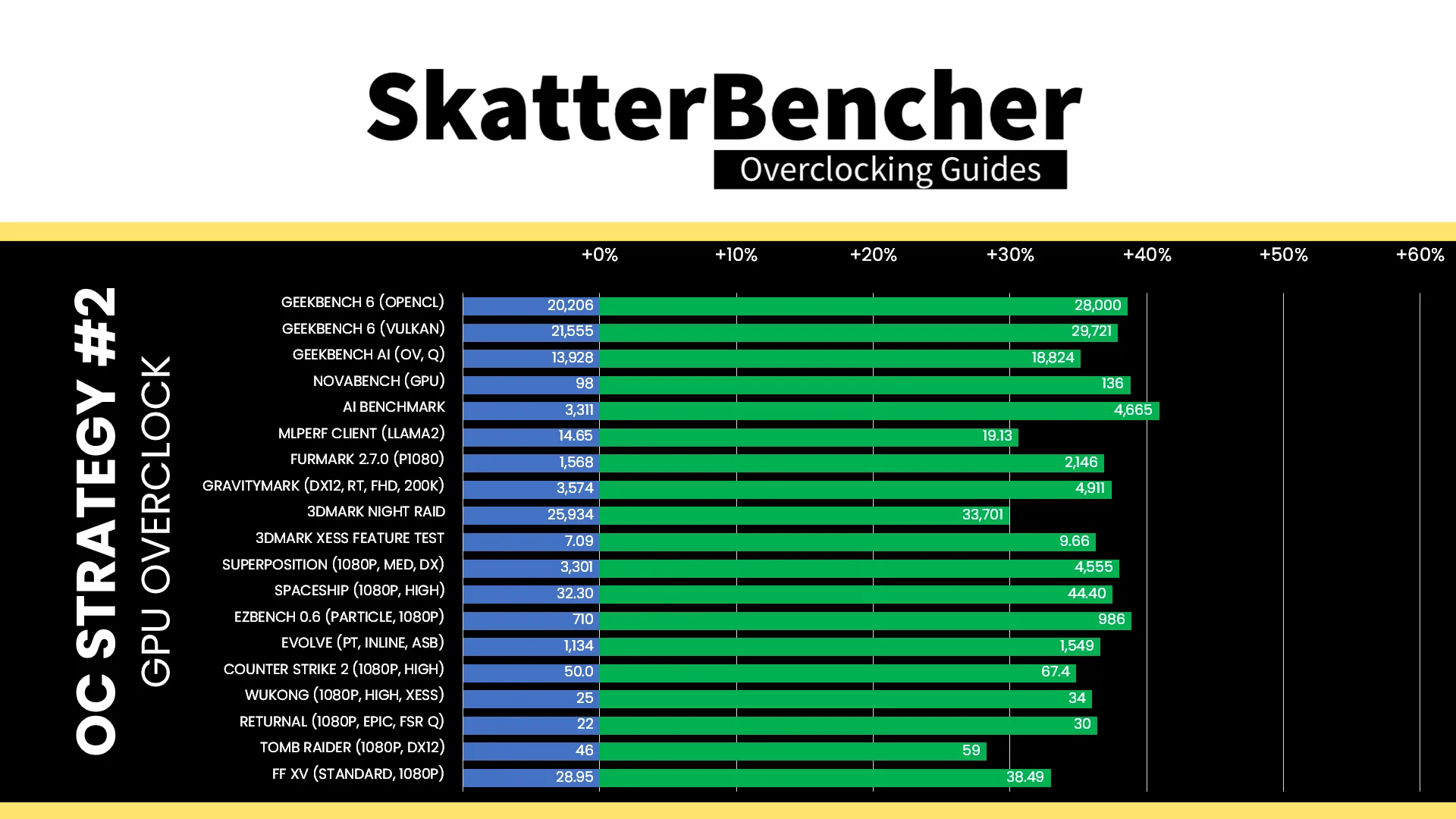
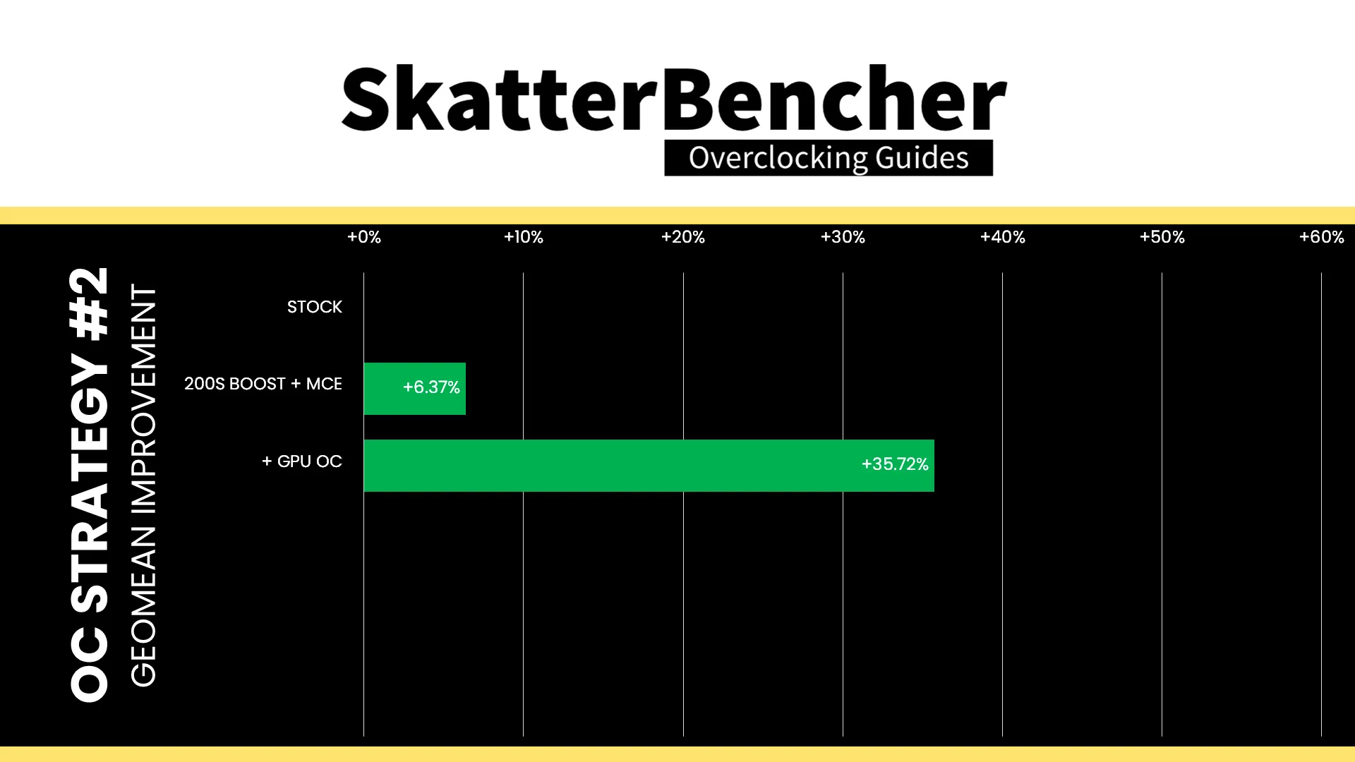
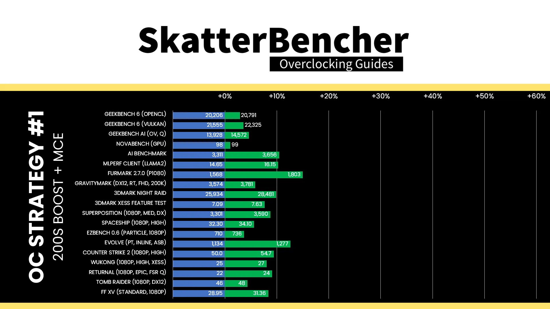
Overclocking the graphics core will, of course, significantly improve the benchmark performance. Perhaps surprisingly, we find that the performance improvement is pretty uniform across the entire benchmark stack. Compute workloads and different types of 3D engines all improve by about 30 to 40%. The Geomean performance improves by nearly 30 percentage points from the previous OC Strategy, and we get a maximum improvement of +40.89% in AI Benchmark.
When running the 3DMark Speed Way Stability Test, the average GPU clock is 2800 MHz with 1.023 volts. The GPU memory clock is 4000 MHz. The average GPU Temperature is 32 degrees Celsius, and the average GPU Cores Power is 15.2 watts.
When running the OCCT 3D Standard Stress Test, the average GPU clock is 2800 MHz with 0.986 volts. The GPU memory clock is 4000 MHz. The average GPU Temperature is 39 degrees Celsius, and the average GPU Cores Power is 27.3 watts.
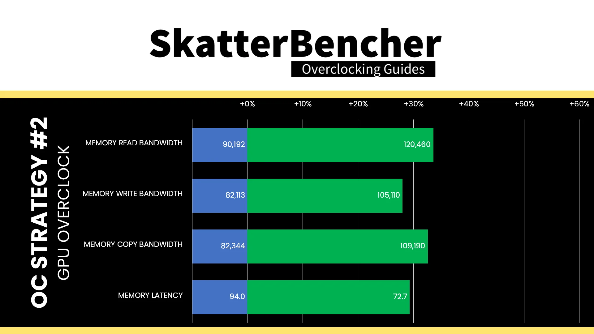
OC Strategy #3: Data Fabric and Memory Subsystem Tuned
In our third overclocking strategy, we delve into tuning the memory subsystem performance.
On Intel Arrow Lake processors, the data fabric and memory subsystem consist of the Ring, the NGU, the D2D interfaces, and the system memory. However, since Arrow Lake introduces the concept of tile-based architecture, we only have to look at the NGU and system memory.
Let me elaborate.
The Ring is integrated on the Compute tile together with the P-cores, E-cores, and last-level cache. Unlike previous architectures, the integrated graphics are no longer connected to the Ring data bus, as the graphics tile is connected to the NGU via a D2D interface.
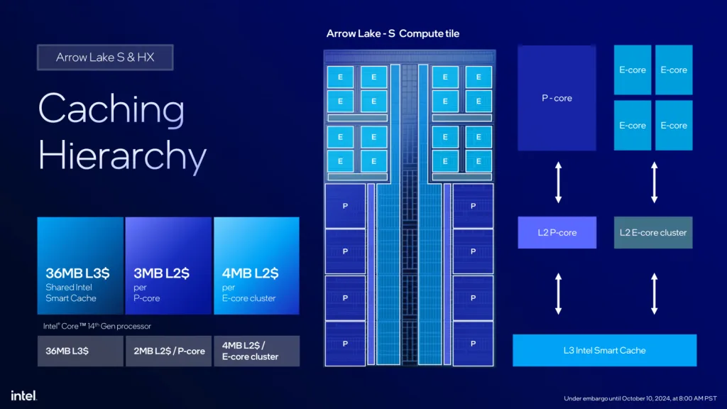
Speaking of which, the graphics tile D2D interface is different from the compute tile D2D interface. Not only is it using a different data protocol (CXL instead of IDI), but its frequency can also not be adjusted by the end-user. As we’ve learned in SkatterBencher #84 when we overclocked the Core Ultra 9 285K, only the CPU D2D interface can be overclocked.
So, we’re left with the NGU and System Memory tuning options.
NGU / NoC
NGU stands for “Next Generation Uncore” and is the successor to the uncore we know from previous generation Intel processors. The NGU fabric – sometimes called sub-system – includes several sub-components such as the network on chip (NoC) and UFI bridges. It’s located on the SoC tile.
On Arrow Lake-S, NGU overclocking is essentially NoC overclocking. The NOC fabric is the primary communication bridge between the various IP blocks on the chip such as the memory controller, the CPU cores (via D2D), and graphics (via D2D).
NGU Clocking Topology
The NGU reference clock frequency is generated internally by the SoC PLL. However, it can also be clocked with an external clock generator providing the reference clock for the SoC PLL. This clock affects nearly all the IP blocks of Arrow Lake, except for those in the Compute Tile (in asynchronous mode) and the PCIe/DMI links.
The reference clock is multiplied by the NGU ratio to achieve the final clock frequency. The default ratio is 26X, which yields a 2.6 GHz operating frequency.
NGU Voltage Topology
The external VccSA MBVR powers several parts of the SOC dielet, including the NGU. Unlike Compute IP, the parts of the SOC dielet are not powered using DLVR. So, power delivery is identical to previous architectures.
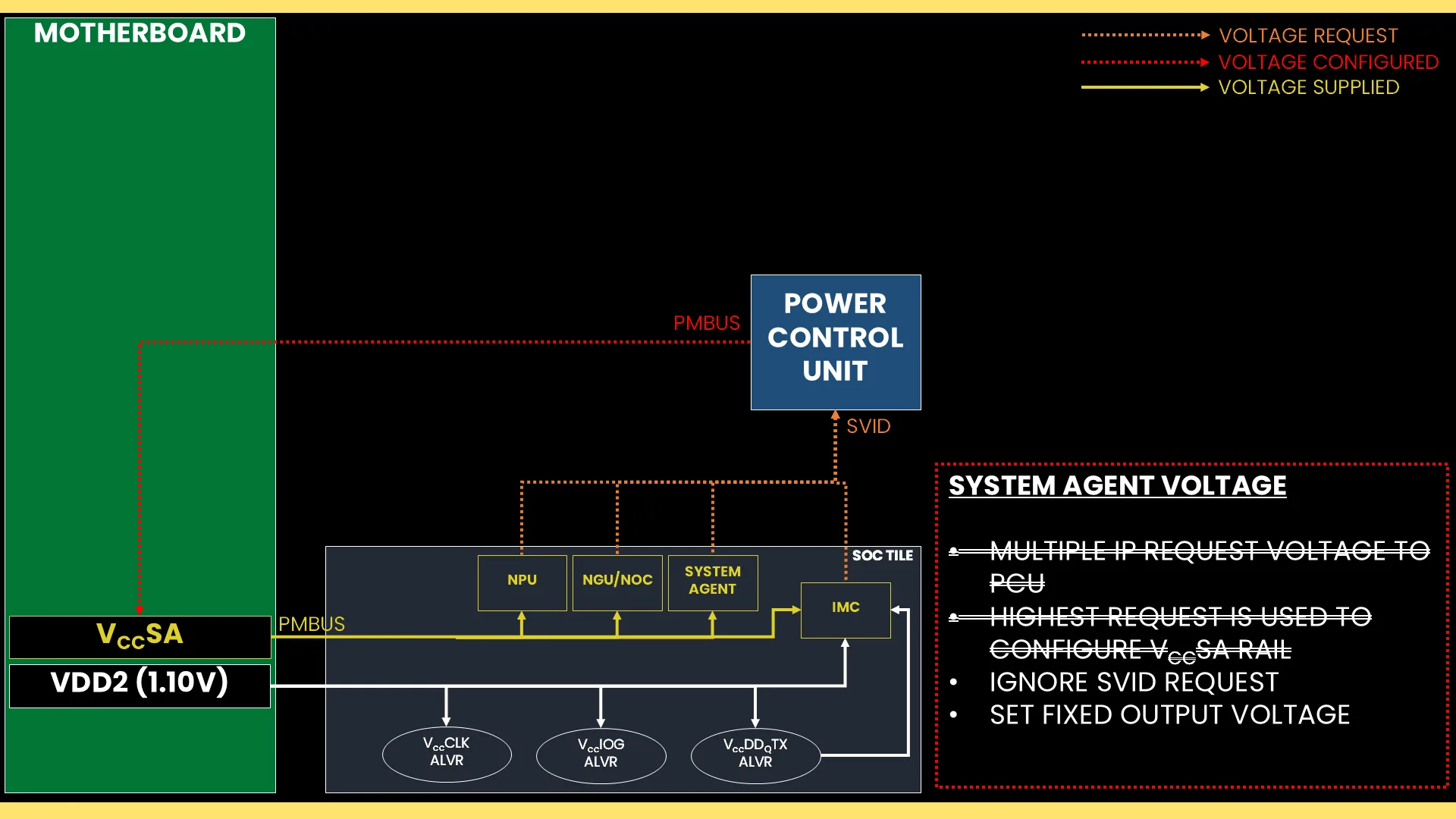
The most relevant parts powered by the VccSA voltage rail are the system agent, the NoC, the NPU, and the memory controller. The voltage configuration of the VccSA voltage rail is rather complicated. Since multiple IP domains share the voltage rail, the VccSA voltage is set based on the highest requested voltage from the various connected IP blocks.
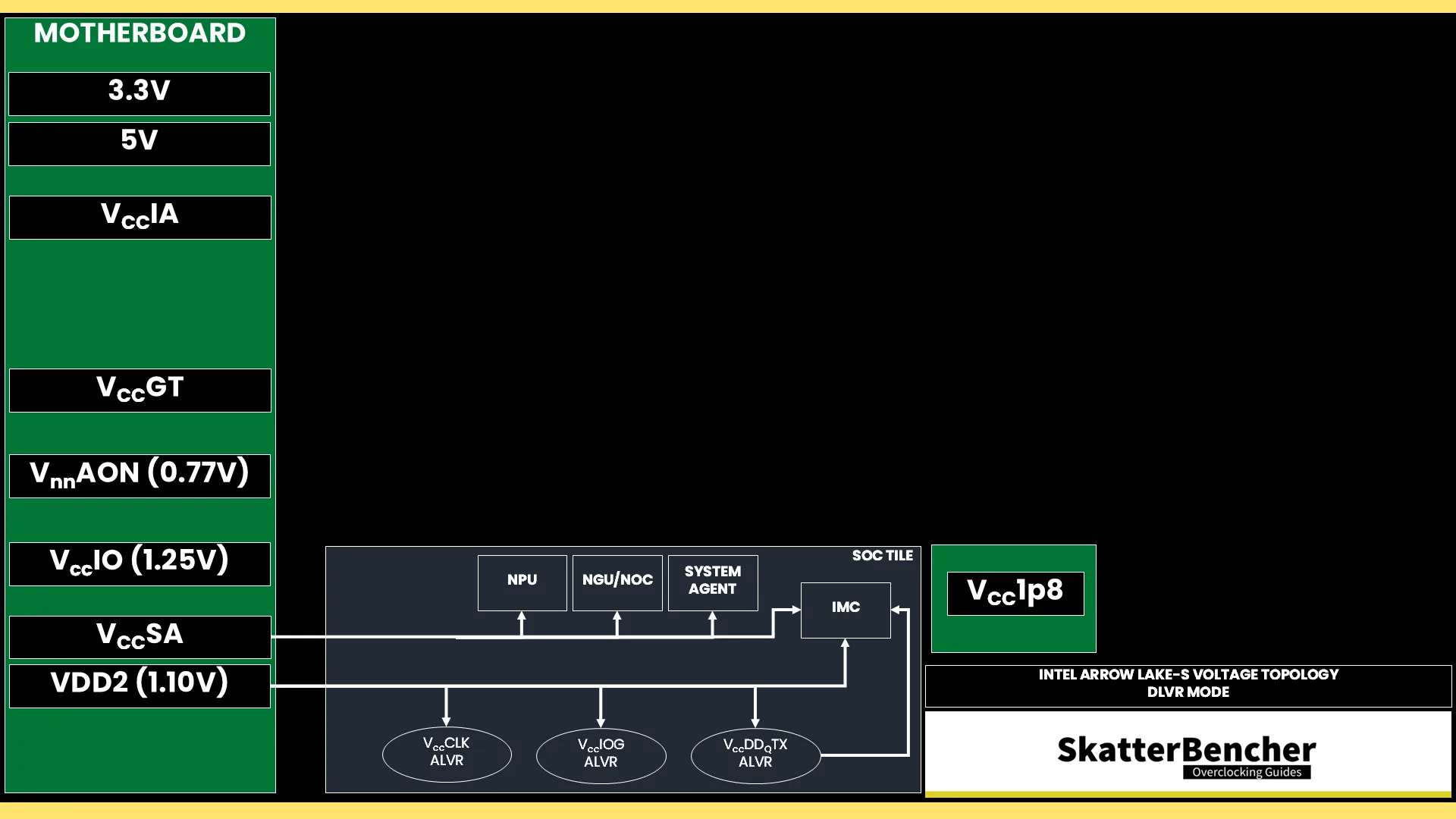
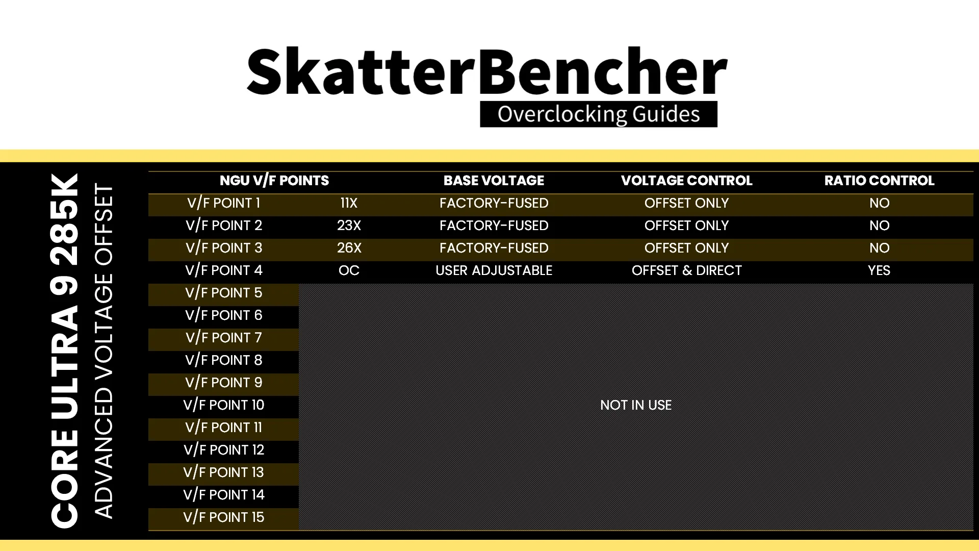
The NoC has its own V/F curve which is defined by up to four (4) V/F work points. The first three (3) V/F points (at 11X, 23X, and 26X) are factory-fused and the last point is mapped to the “OC Ratio.” Based on the work points, the NGU requests an operating voltage from the VccSA voltage rail using the SVID protocol.
However, there is a second way to voltage configuration: ignore the SVID voltage requests and calculations, and program the VccSA voltage regulator directly over PMBus. This process effectively allows us to take full control over the voltage set by the VccSA voltage rail.
System Memory Timings Tuning
The last piece of the memory subsystem performance tuning is the memory timings. For this part, I rely on ASUS’ Memory Presets technology.
ASUS Memory Presets
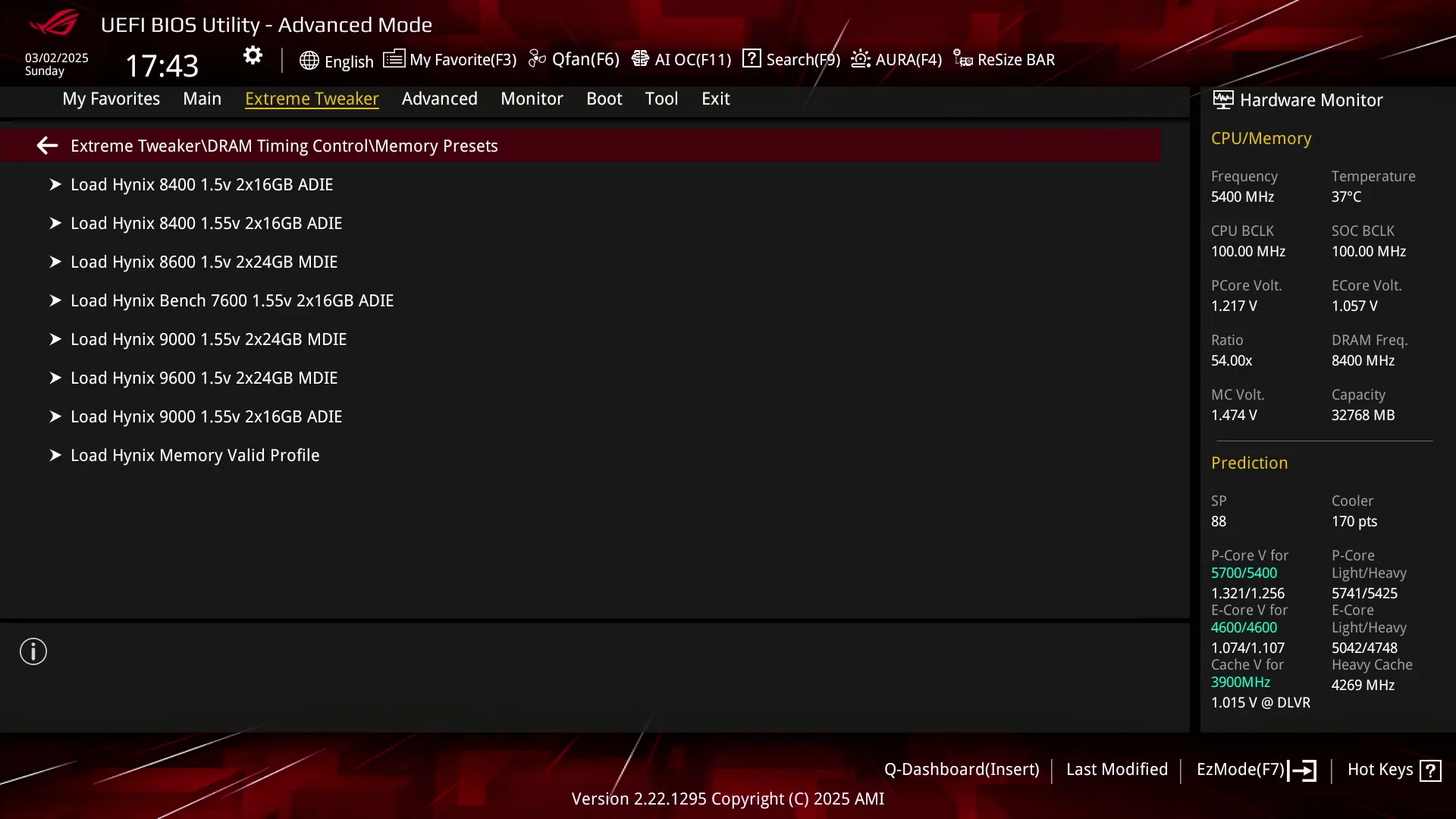
ASUS Memory Presets is an ASUS overclocking technology that provides a selection of memory-tuning presets for specific memory ICs. The presets will adjust the memory timings and voltages. On the ASUS ROG Z890 Apex motherboard (BIOS 0041) there are 8 presets available for Hynix 2x16GB and 2x24GB memory. I loaded the Hynix 8600 2x24GB profile for my testing.
This memory profile also sets the memory voltage to 1.5V, which would fall outside the 200S Boost specification. So, to maintain the configuration from the previous OC Strategy, I set the DRAM VDD and VDDQ voltage back to 1.4V. Fortunately, the memory preset worked straight out of the box and no further adjustments were required to achieve stability.
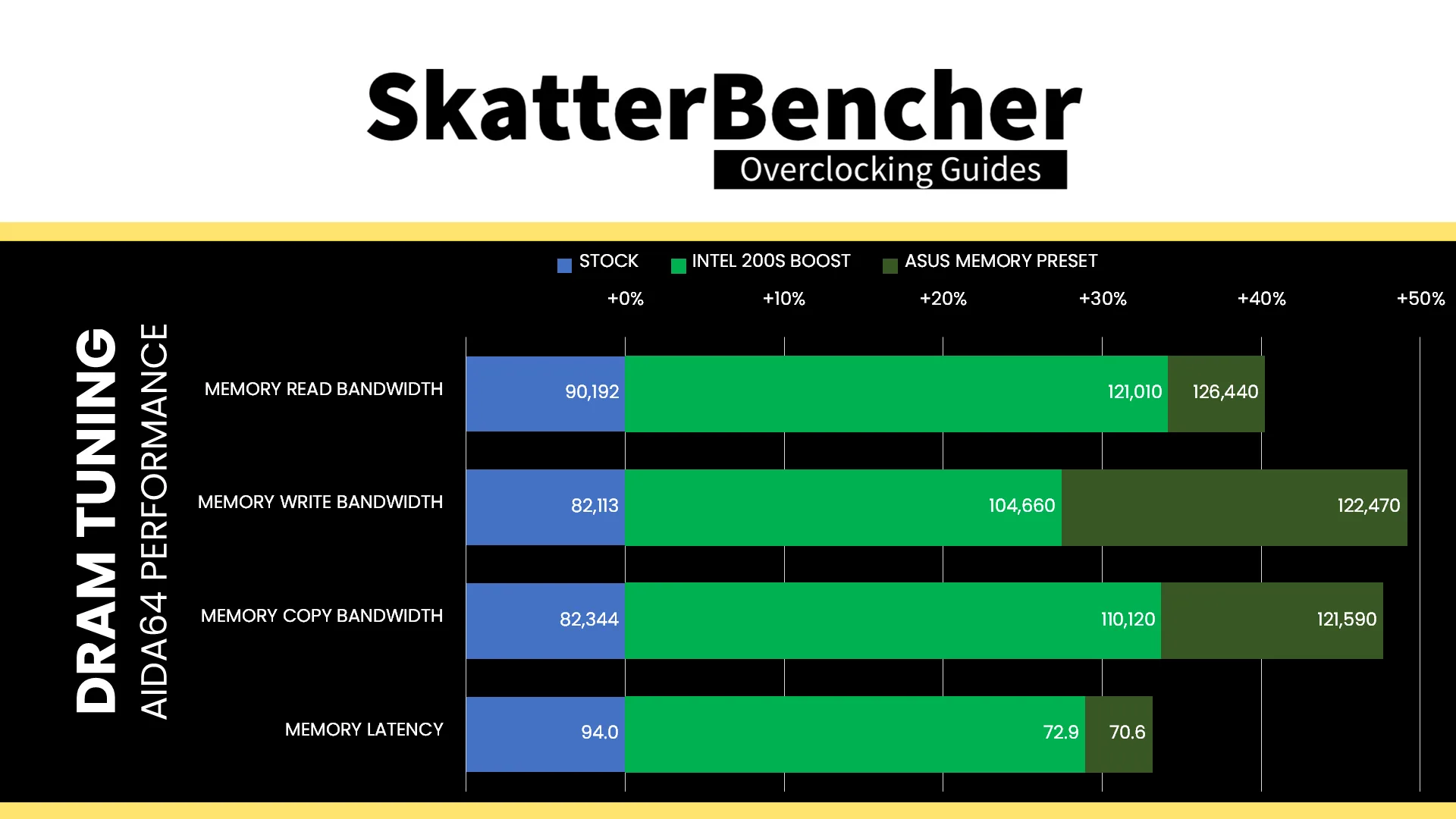
After the tuning, our AIDA64 performance improved quite significantly. We got about +30% extra bandwidth and lower latency by enabling Intel 200S Boost. The ASUS Memory Preset tuning then added another 5-20% on top of that.
BIOS Settings & Benchmark Results
Upon entering the BIOS
- Go to the Extreme Tweaker menu
- Set Performance Preferences to ASUS Advanced OC Profile
- Set Ai Overclock Tuner to XMP I
- Set ASUS MultiCore Enhancement to Enabled – Remove All Limits
- Enter the DRAM Timing Control submenu
- Enter the Memory Presets submenu
- Load the Hynix 8600 1.5v 2x24GB MDIE profile
- Leave the Memory Presets submenu
- Enter the Memory Presets submenu
- Leave the DRAM Timing Control submenu
- Set Max. CPU Graphics Ratio to 56
- Set NGU Ratio to 34
- Set CPU System Agent Voltage to Manual Mode
- Set CPU System Agent Voltage Override to 1.300
- Set DRAM VDD to 1.400
- Set DRAM VDDQ to 1.400
Then save and exit the BIOS.
We re-ran the benchmarks and checked the performance increase compared to the default operation.
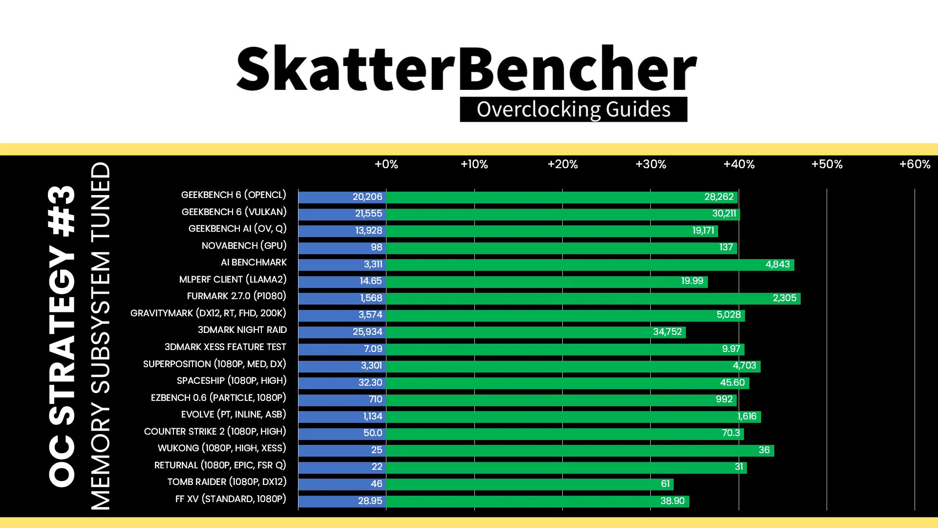
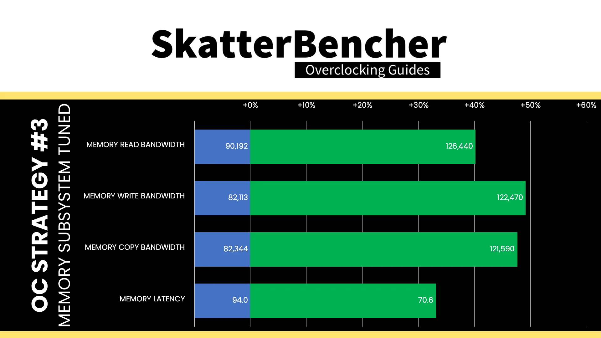
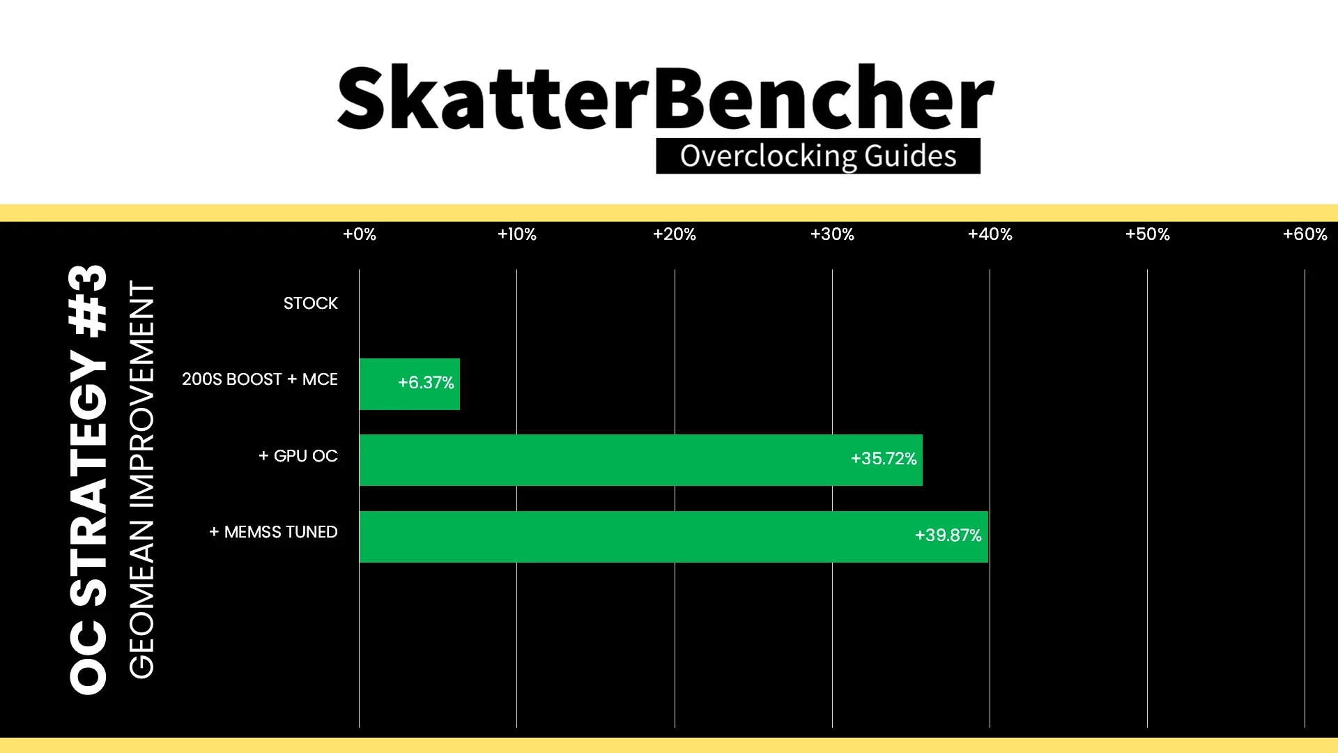
Similar to what we’ve seen with other modern integrated graphics, the memory sub-timings can have a small but noticeable impact on compute performance. Especially in workloads that are memory-intensive like modern games and machine learning. The Geomean performance improves another four percentage points, and we get a maximum improvement of +47.00% in Furmark.
When running the 3DMark Speed Way Stability Test, the average GPU clock is 2800 MHz with 1.023 volts. The GPU memory clock is 4000 MHz. The average GPU Temperature is 33 degrees Celsius, and the average GPU Cores Power is 15.6 watts.
When running the OCCT 3D Standard Stress Test, the average GPU clock is 2800 MHz with 0.986 volts. The GPU memory clock is 4000 MHz. The average GPU Temperature is 40 degrees Celsius, and the average GPU Cores Power is 27.2 watts.
OC Strategy #4: GPU PMBUS Mode
In the fourth overclocking strategy, we look to maximize the GPU overclock by increasing the operating voltage. But that’s not without problems and we must switch from SVID to PMBus mode to avoid any performance throttling.
Before we jump into the nitty gritty of PMBus mode, let’s have a closer look at the Intel Graphics voltage topology.
Intel Graphics (Arrow Lake) Voltage Topology
The external VccGT MBVR exclusively provides the voltage rail for Arrow Lake integrated graphics. Unlike the Compute IP blocks, the integrated graphics doesn’t use DLVR. So, the power delivery is identical to the previous architecture: straight from the VccGT rail to the graphics cores. We can refer to it as Power Gate (PG) mode.

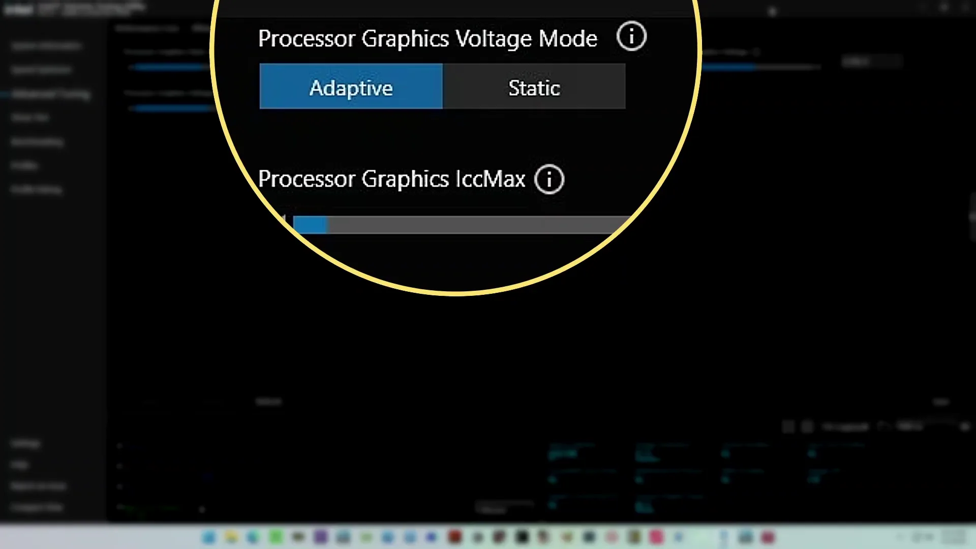
VccGT Power Gate SVID Mode
Based on its V/F curve, the integrated graphics request an operating voltage using the SVID protocol from the CPU Power Control Unit (PCU). The PCU in turn configures the VccGT voltage rail. There are two ways to configure the graphics voltage:
- Adaptive mode (+offset)
- Override mode (+offset)
The way these options work for Intel Graphics on Arrow Lake CPUs is, unfortunately, completely different than prior generation Intel integrated graphics. As I mentioned earlier in the guide – the behavior resembles Arc discrete graphics.
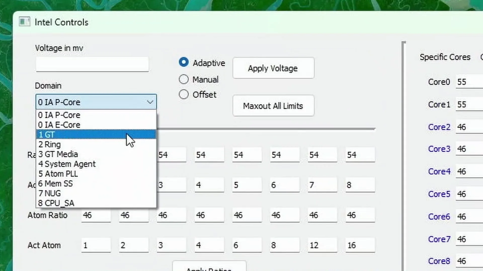
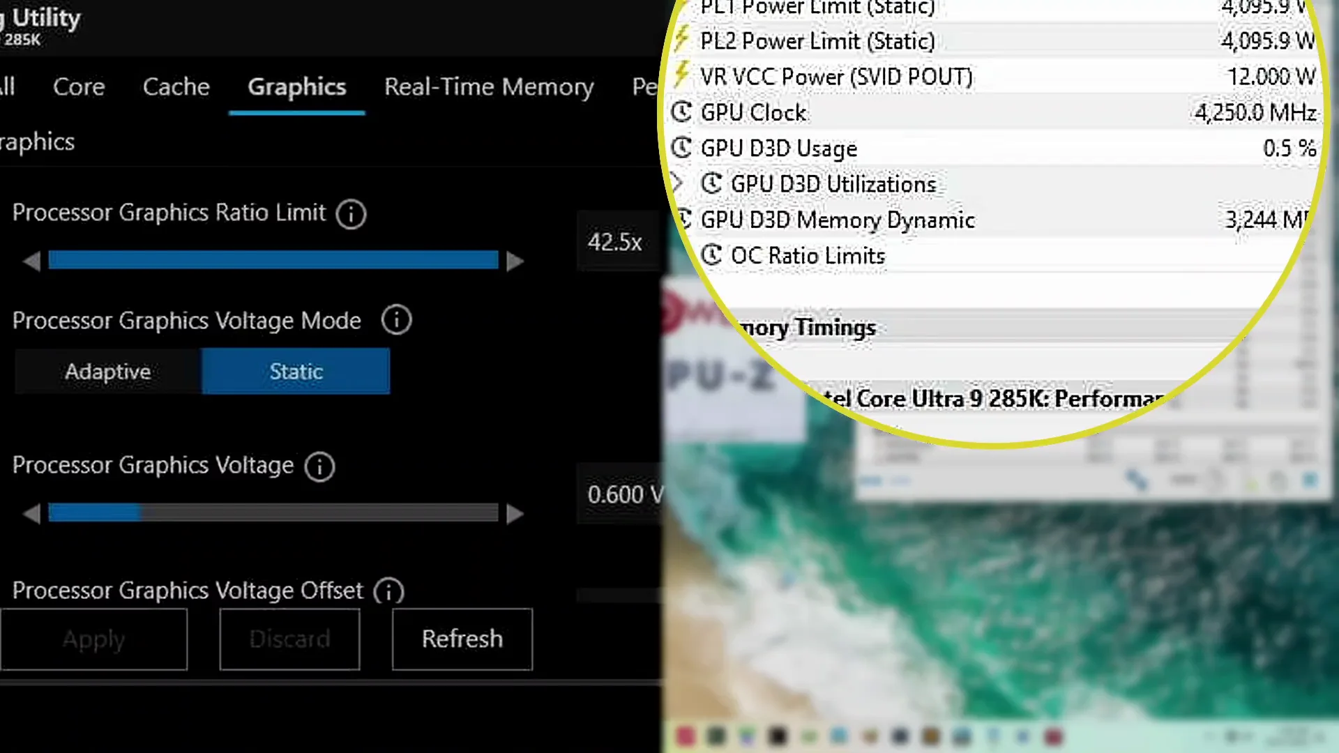
Also, the VccGT SVID configuration options are not available in the ASUS ROG BIOS. However, you can still access it using Shamino’s OC tool or Intel Extreme Tuning Utility.
Under- and Overvolting
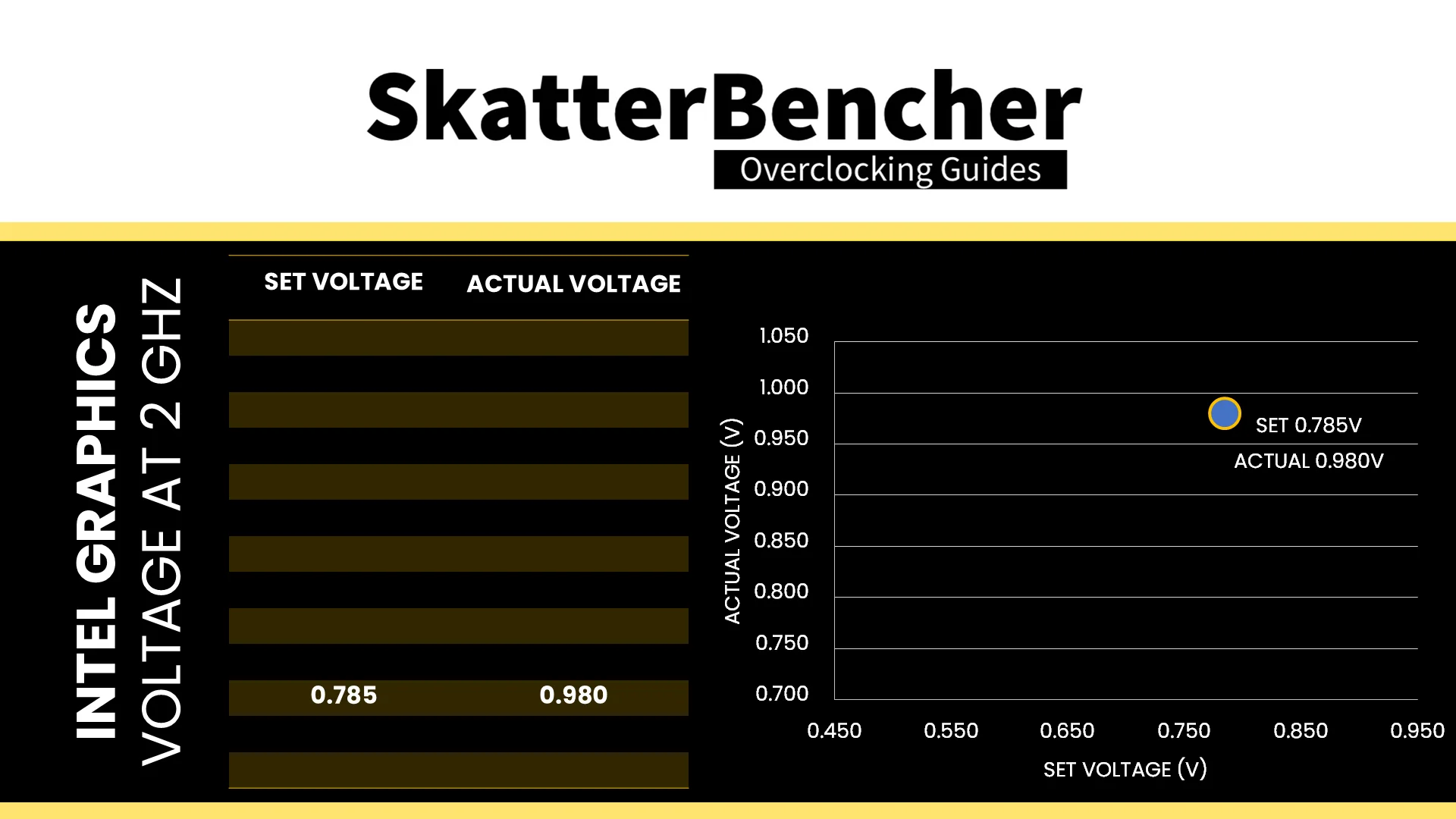
As you may remember from SkatterBencher #64 in which I overclocked the Arc A770, the voltage set doesn’t match the actual voltage. And that’s the same for our Alchemist-based Intel Graphics for Arrow Lake. In XTU we find the “set” voltage to be 785 mV. However, the actual voltage at 2 GHz is 980 mV – about 200 mV higher.
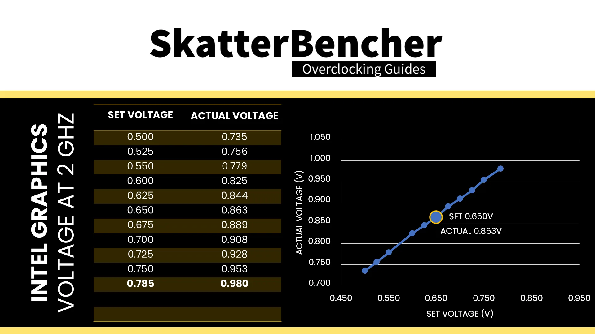
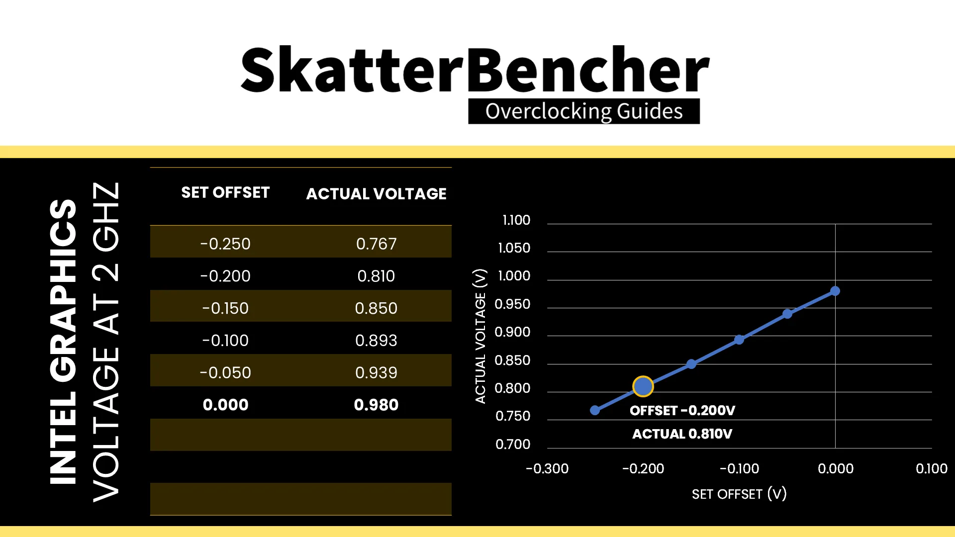
By reducing the set voltage, we effectively undervolt the entire voltage-frequency curve. For example, setting 650 mV yields an effective voltage of 863 mV at 2 GHz. Strangely enough, we can also undervolt the V/F curve by using the voltage offset tool. For example, undervolting by 200 mV gives us an effective voltage of 810 mV.
Using the same tools, we can also overvolt – which is what we’re interested in to squeeze higher performance. But, again, we run into a similar problem to the Arc A770: GPU Voltage Frequency Throttling.
GPU Voltage Frequency Throttling
Similar to Arc A770 and Arc A380, there’s a maximum allowed voltage for the Intel Graphics. For the A770 it was 1.2V, for the Arc A380 it was 1.175V, but for Intel Graphics it’s only about 1.050V. I can easily demonstrate this by switching the voltage to static mode and tracking the GPU frequency as we increase the voltage.
Up until a set voltage of 800 mV, which gives an effective voltage of 1.02V, the frequency is stable at 2500 MHz. But once we go beyond that set voltage, the frequency gradually starts dropping until we reach 100 MHz.
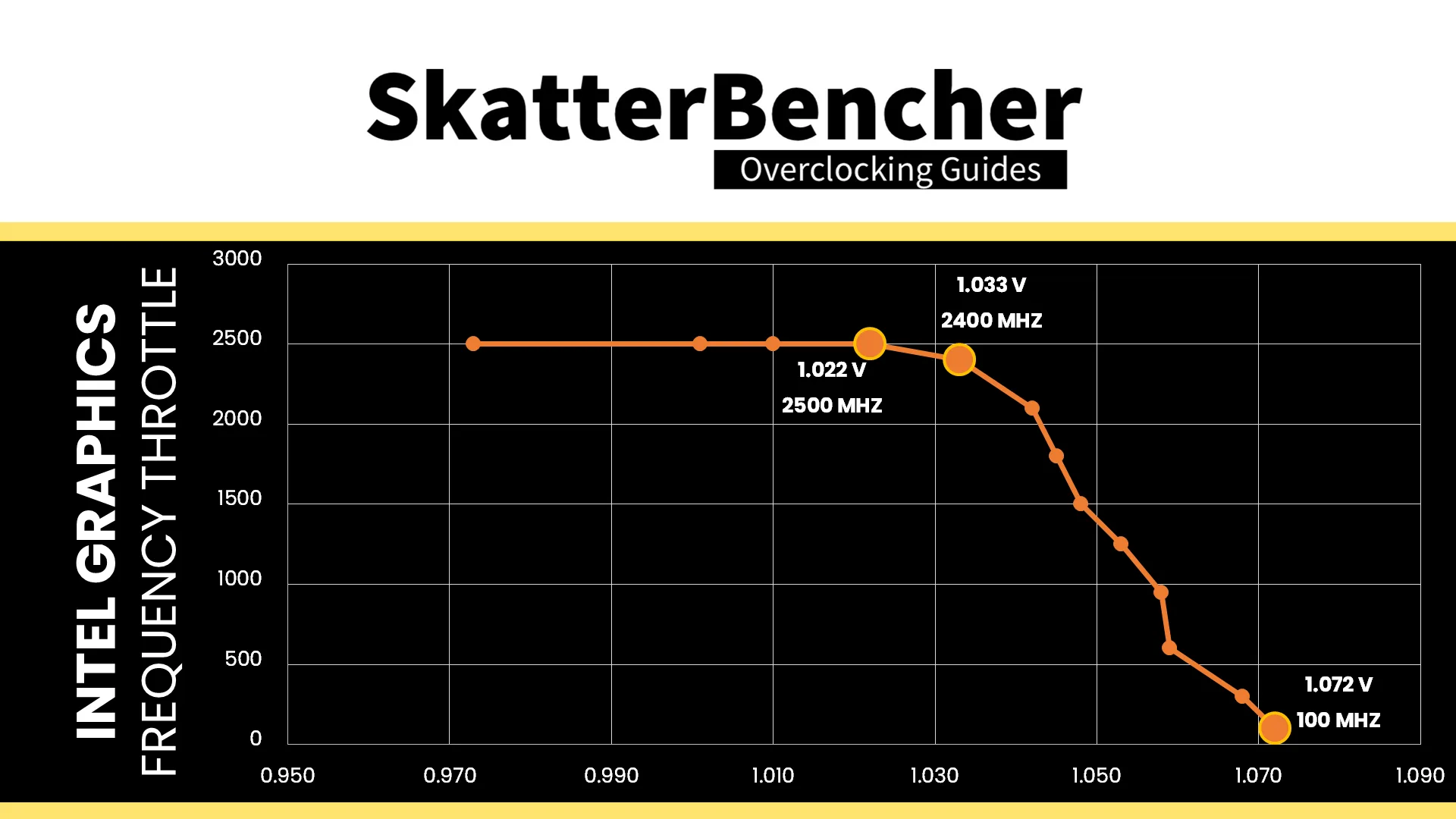
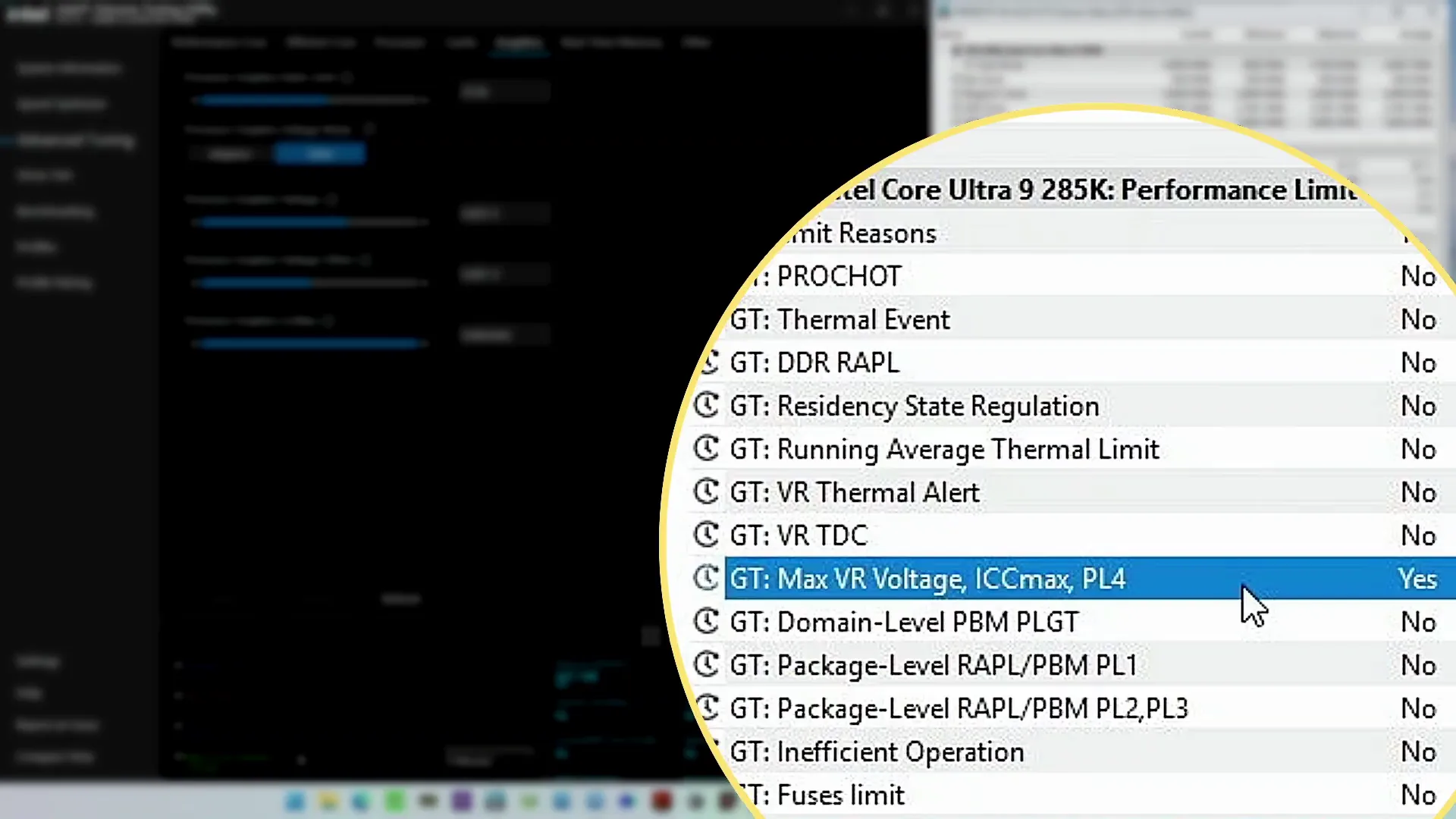
You can also check the HWiNFO GT Limit Reasons. When the frequency is capped due to the voltage limit, it’ll flag the Max VR Voltage limiter.
VccGT Power Gate PMBus Mode
As mentioned, the VccGT SVID mode configuration is not available in the ASUS ROG BIOS. And even if it was, we’d run into performance limiter issues.
However, that doesn’t mean we can’t configure the graphics voltage as, fortunately, there’s a second way to approach Power Gate Mode voltage configuration: ignore the SVID voltage requests and calculations, and program the VccGT voltage regulator directly over PMBus. This process effectively allows us to take full control over the voltage set by the VccGT voltage rail.

This approach is a very traditional way of overclocking whereby you set a fixed output voltage and then use an appropriate VRM load line setting – if available – to reduce the operating voltage in higher load scenarios. The load line configuration isn’t particularly useful for integrated graphics.
A key advantage of using PMBus mode is that we completely ignore the SVID voltage request to manage the operating voltage, however we don’t disable the SVID functionality. That means we can force the SVID voltage to be configured to a really low value while maintaining a high output voltage. This effectively works around any performance limiter that relies on SVID information. Normally, we’d need to set the SVID manually to a low value, but for the Z890 Apex motherboard that’s already a BIOS auto-rule.

Now we can freely increase the VccGT voltage as high as we want to maximize our overclock.
Intel Graphics (Arrow Lake) PMBus Overclocking Process
Using the same process from OC Strategy #2 we can figure out what’s the highest possible frequency with elevated voltages.
I first tried 1.3V which yielded a stable frequency of 3100 MHz. That’s surprisingly poor voltage scaling considering 2.8 GHz was stable at about 1V. Higher voltage also didn’t seem to yield much higher frequency – even 1.4V wasn’t enough to run 3.2 GHz. So, I stuck with 1.3V for this overclocking strategy.
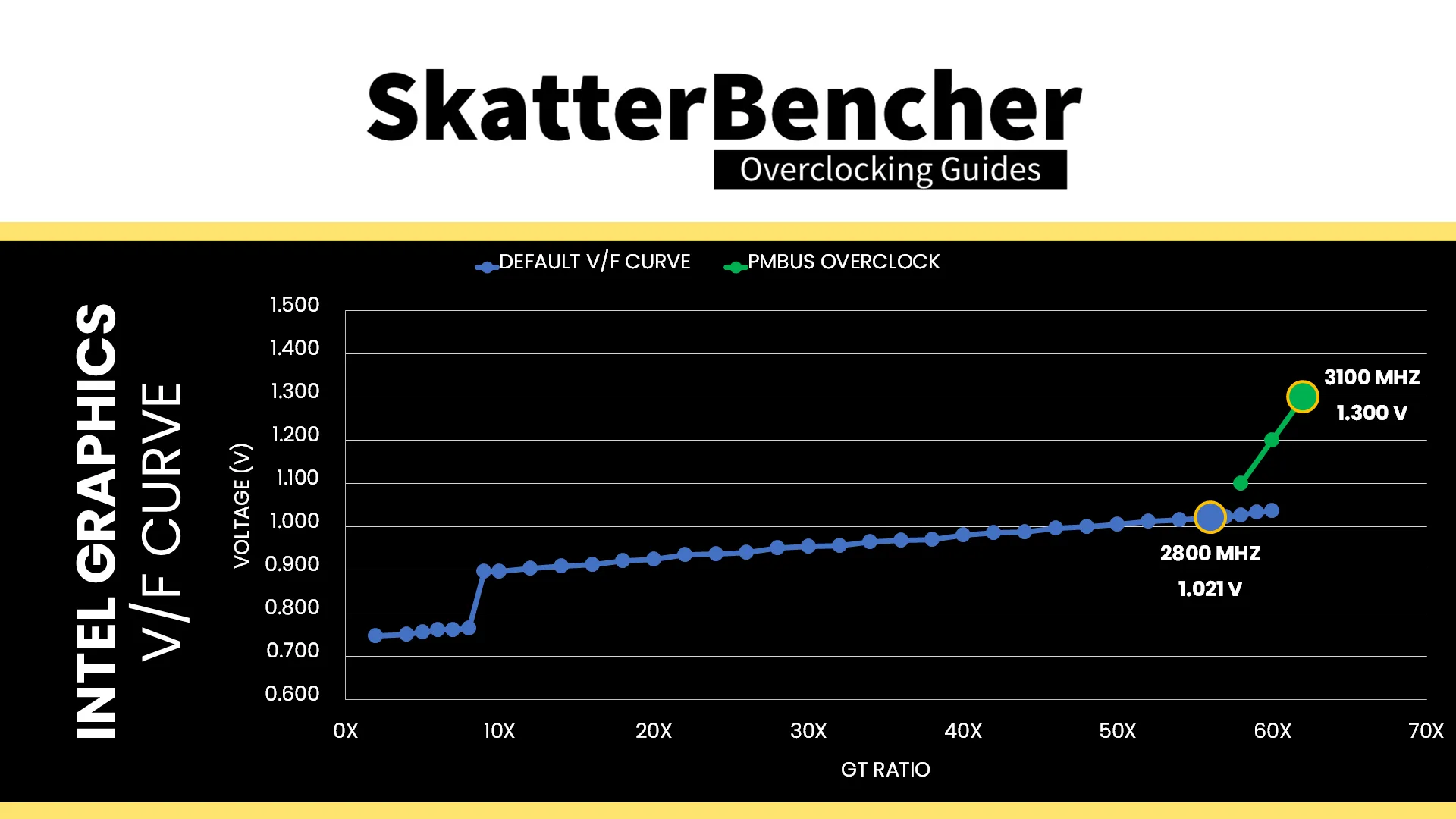
Plotting the PMBus overclocking results next to the default V/F curve graph, it seems almost impossible that the voltage scaling is this poor. But the default V/F curve is deceptive because, as it turns out, it’s far from an optimized curve.
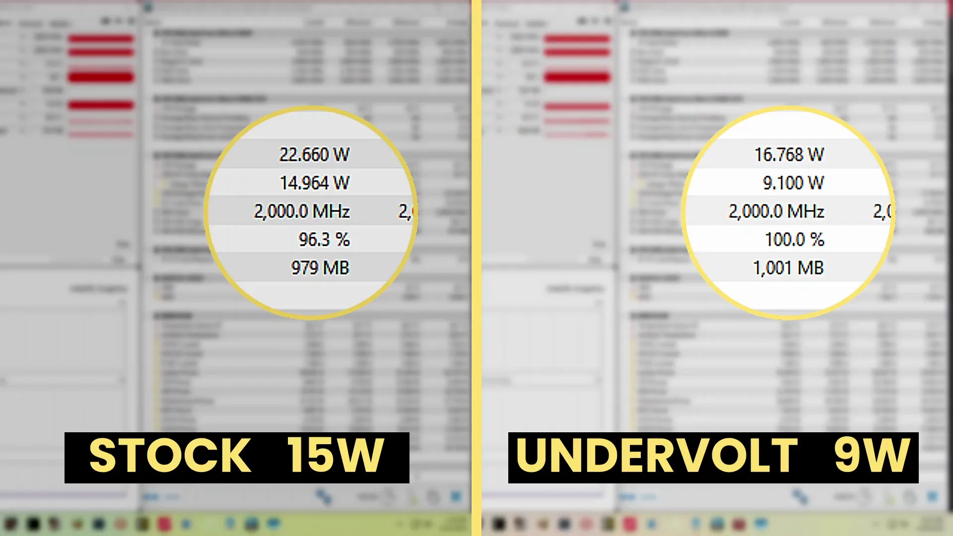
Playing around with the undervolting capabilities, I quickly found that there’s an incredible amount of undervolting headroom around the stock operating frequency. In fact, about 250 mV headroom at 2 GHz. And if we plot a couple additional data points, it becomes much more understandable why we’re seeing such poor voltage scaling beyond 3 GHz as our manual voltage control results fall in line with the undervolted V/F curve.
I don’t want to dwell on this too much but the undervolting headroom is pretty astonishing. Out of curiosity I also ran the OCCT stress test with a big 20% undervolt. The result: a 40% reduction in power consumption from about 15W to 9W.
BIOS Settings & Benchmark Results
Upon entering the BIOS
- Go to the Extreme Tweaker menu
- Set Performance Preferences to ASUS Advanced OC Profile
- Set Ai Overclock Tuner to XMP I
- Set ASUS MultiCore Enhancement to Enabled – Remove All Limits
- Enter the DRAM Timing Control submenu
- Enter the Memory Presets submenu
- Load the Hynix 8600 1.5v 2x24GB MDIE profile
- Leave the Memory Presets submenu
- Enter the Memory Presets submenu
- Leave the DRAM Timing Control submenu
- Set Max. CPU Graphics Ratio to 62
- Set NGU Ratio to 34
- Set CPU Graphics Voltage to Manual Mode
- Set CPU Graphics Voltage Override to 1.300
- Set CPU System Agent Voltage to Manual Mode
- Set CPU System Agent Voltage Override to 1.300
- Set DRAM VDD to 1.400
- Set DRAM VDDQ to 1.400
Then save and exit the BIOS.
We re-ran the benchmarks and checked the performance increase compared to the default operation.
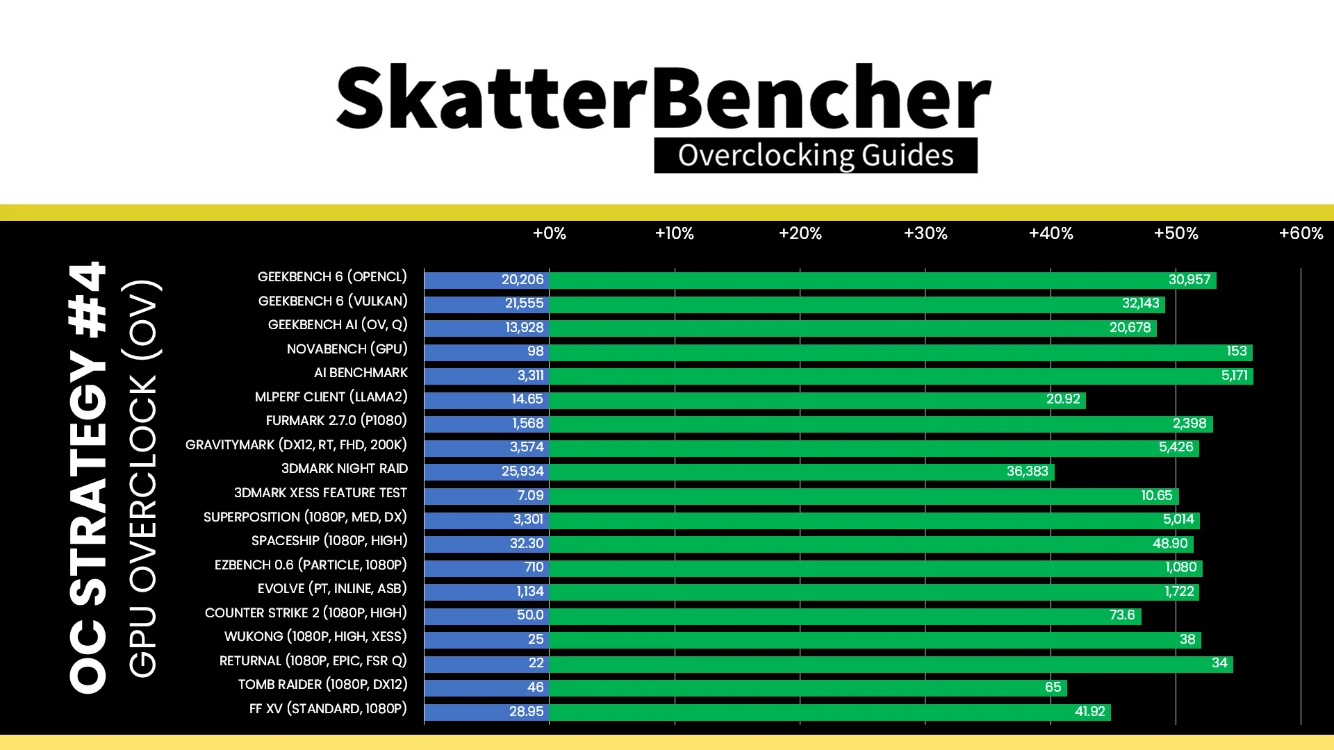

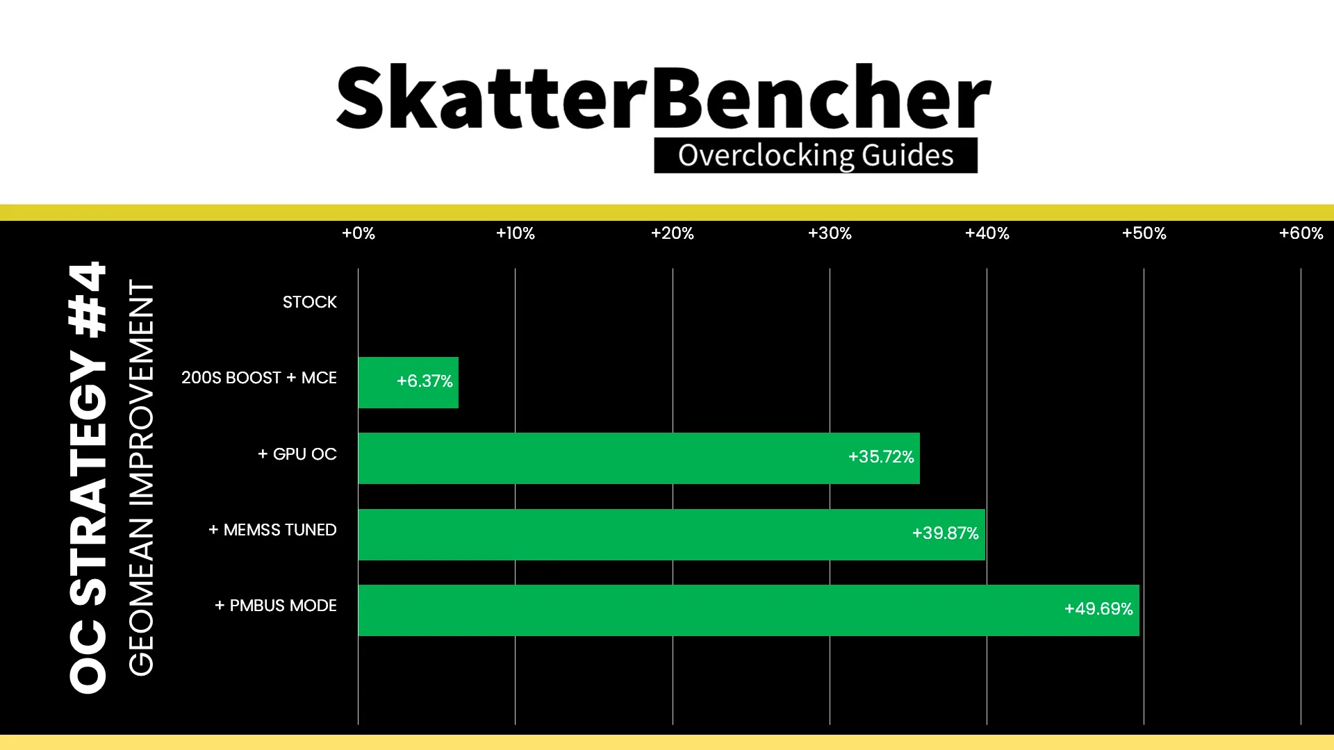
With the help of the increased voltage, we’re able to further increase the GPU overclock by another 10%. That translates into another significant performance uplift across the board. The Geomean performance improves ten percentage points to +49.69% over stock, and we get a maximum improvement of +56.18% in AI Benchmark.
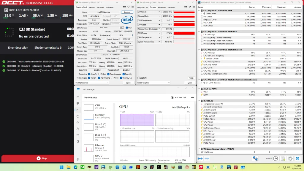
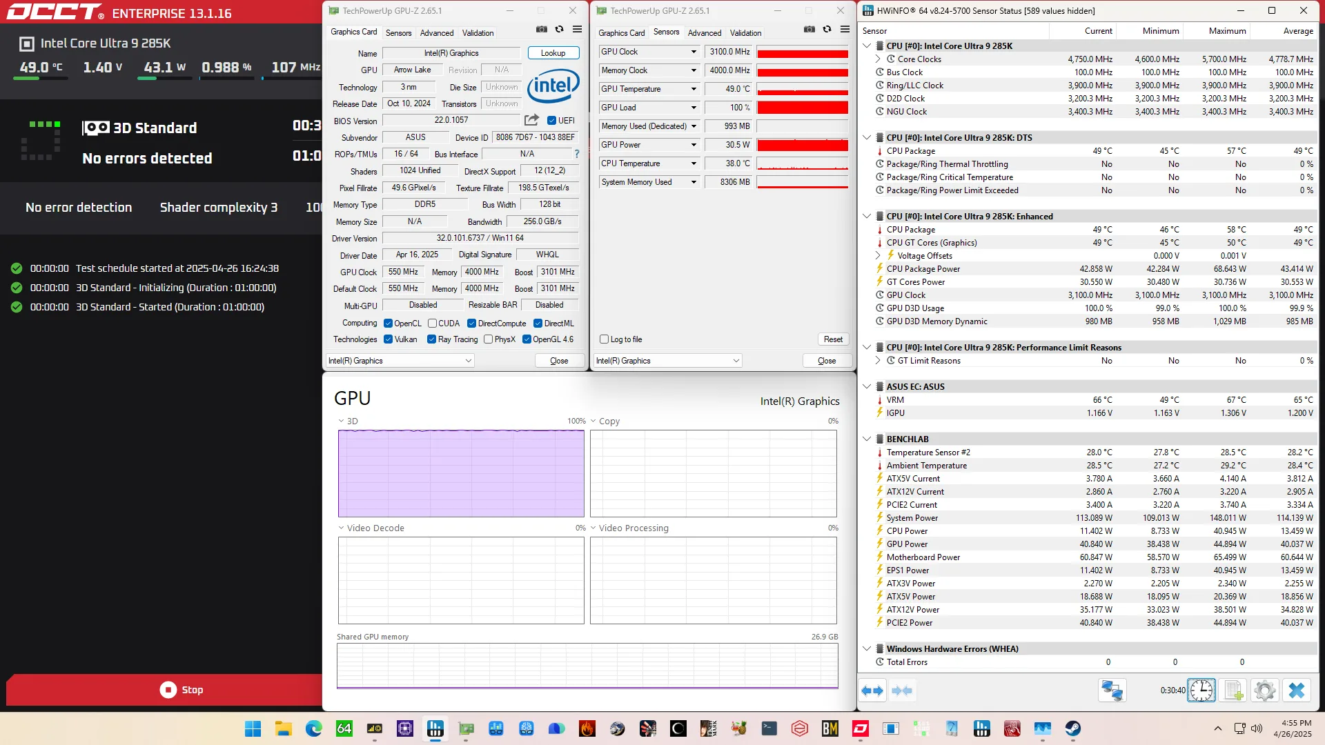
When running the 3DMark Speedway Stability Test, the average GPU clock is 3100 MHz with 1.249 volts. The GPU memory clock is 4000 MHz. The average GPU Temperature is 39 degrees Celsius, and the average GPU Cores Power is 18.8 watts.
When running the OCCT 3D Standard Stress Test, the average GPU clock is 3100 MHz with 1.200 volts. The GPU memory clock is 4000 MHz. The average GPU Temperature is 49 degrees Celsius, and the average GPU Cores Power is 30.6 watts.
OC Strategy #5: BCLK Overclock
In our final overclocking strategy, we have a look at BCLK overclocking. But why?
Why BCLK overclocking?
On previous Intel platforms, BCLK overclocking was a must to push the integrated graphics to the max. That’s because the graphics ratio was limited to 42X, meaning the graphics frequency was limited to 2.1 GHz. I illustrated this in SkatterBencher #57 where I needed 125 MHz BCLK frequency to overclock the Intel UHD Graphics 770 to 2500 MHz.
For Arrow Lake, Intel has extended the range to 85X, meaning we have a maximum frequency of 4250 MHz. While that’s possible to achieve using extreme cooling, it’s a large enough range for ambient cooling. So why try BCLK overclocking?
The main reason I wanted to try BCLK overclocking is to see if it would also increase the Graphics D2D interface. To explain, let’s have a more detailed look at the clocking topology.
Intel Graphics (Arrow Lake) Clocking Topology (Part 2)
As I already mentioned, the 100MHz reference clock for the graphics tile is generated internally by the SoC PLL and then divided by two to achieve a 50 MHz base clock frequency for the graphics cores.
However, the SoC reference clock can also be provided by an external clock generator. This reference clock affects nearly all Arrow Lake IP blocks, except for those in the Compute Tile and the PCIe/DMI links. The Compute Tile IP can be linked to this reference clock in “synchronous mode” or remain independent if you keep it in “asynchronous mode.” For our purpose, it makes sense to stay in asynchronous mode since we don’t want to adjust the CPU P-core and E-core frequency.
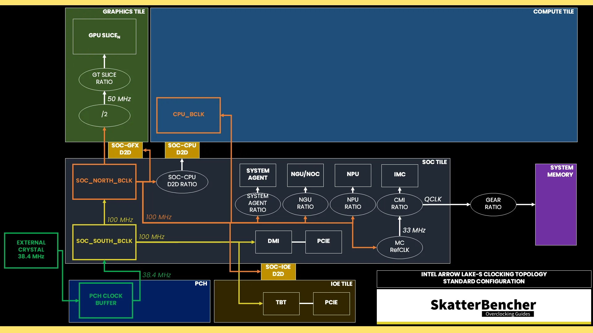
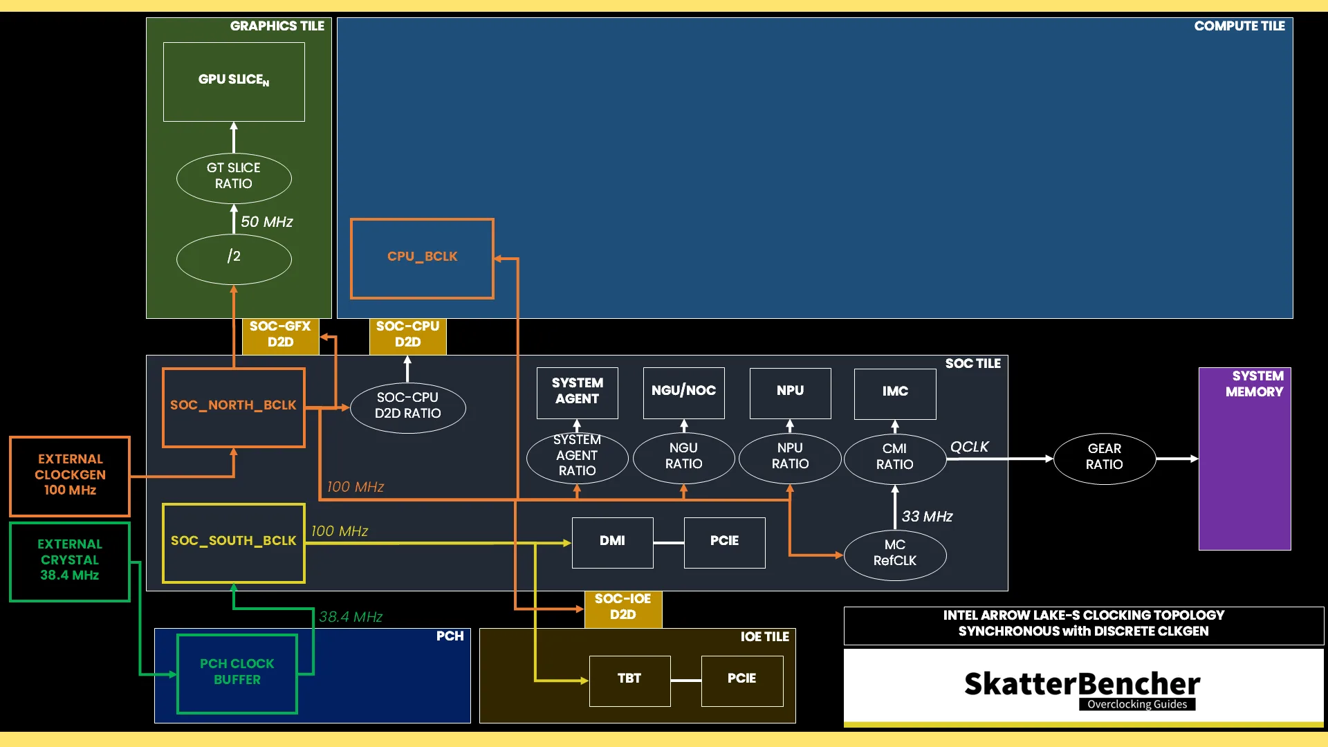
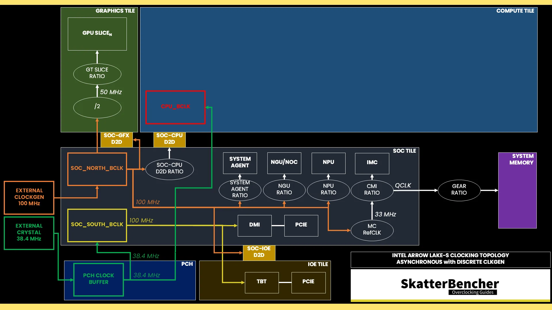
Before we start pushing the SoC reference clock, it’s important to take note of all the IP blocks that will be affected by this frequency:
- CPU-D2D (D2DPLL/S2CPLL) & GFX-D2D (G2SPLL/S2GPLL)
- NGU (NCLKPLL) & System Agent IP like Display Engine (DEPLL), NPU (IUNITPUPLL), Media (MEDIAPLL), and VPU (VPUPLL)
- IMC (CMIPLL) & System Memory (DDRPLL)
The operating frequency of some of these IP blocks – like the NPU and VPU – can’t be adjusted, so they’ll be the limiting factor when pushing the SoC reference clock. They are powered by the VccSA voltage rail, so increasing the SA voltage may help improve stability to a certain extent.
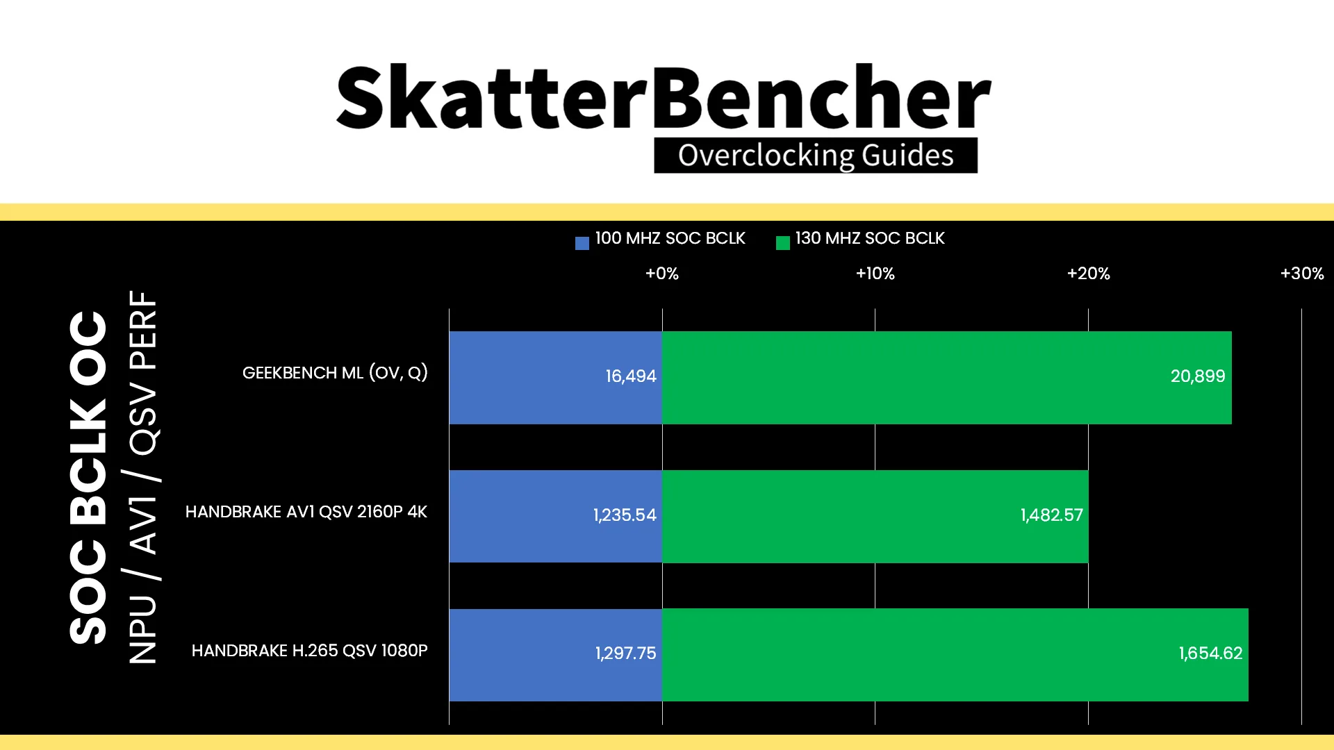
To illustrate the impact of SoC reference clock overclocking on the NPU and VPU, I quickly checked the performance in Geekbench AI for inference with the NPU and Handbrake for AV1/QSV encoding. As you can see, after increasing the BCLK frequency to 130 MHz (+30%), the performance also increased by about 30%.
Intel Graphics (Arrow Lake) BCLK Overclocking Process
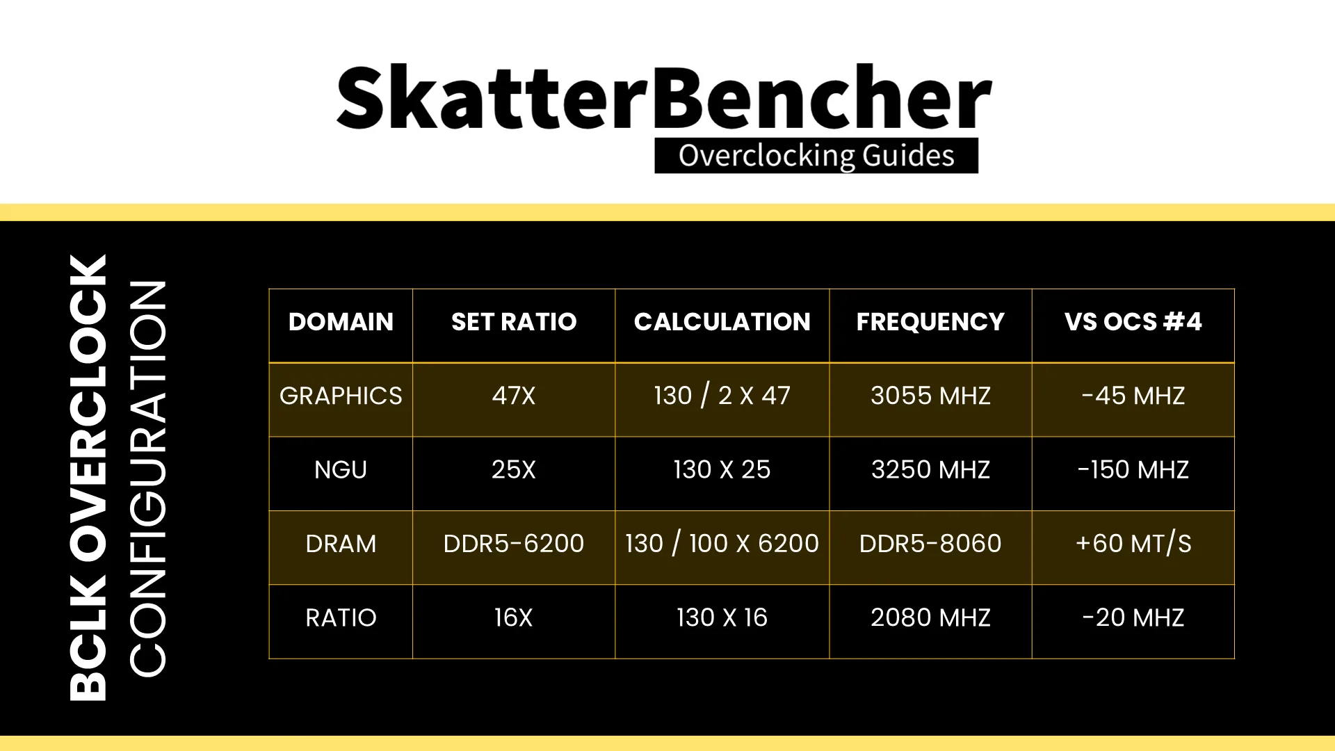
To keep things simple, I targeted the same frequencies and voltages as used in OC Strategy #4. So,
- Graphics Ratio: 47X, resulting in 3055 MHz (130 MHz / 2 x 47)
- NGU Ratio: 25X, resulting in 3250 MHz (130 MHz x 25)
- DRAM Ratio: DDR5-6200, resulting in DDR5-8060 (130 MHz / 100 x 6200)
- D2D Ratio: 16X, resulting in 2080 MHz (130 MHz x 16)
BIOS Settings & Benchmark Results
Upon entering the BIOS
- Go to the Extreme Tweaker menu
- Set Performance Preferences to ASUS OC Profile
- Set Ai Overclock Tuner to XMP I
- Set BCLK Mode to Asynchronous
- Set SOC BCLK Frequency to 130
- Set ASUS MultiCore Enhancement to Enabled – Remove All Limits
- Set DRAM Frequency to DDR5-8060
- Enter the DRAM Timing Control submenu
- Enter the Memory Presets submenu
- Load the Hynix 8600 1.5v 2x24GB MDIE profile
- Leave the Memory Presets submenu
- Enter the Memory Presets submenu
- Leave the DRAM Timing Control submenu
- Set Max. CPU Graphics Ratio to 47
- Set NGU Ratio to 25
- Set BCLK Aware Adaptive Voltage to Enabled
- Set CPU Graphics Voltage to Manual Mode
- Set CPU Graphics Voltage Override to 1.300
- Set CPU System Agent Voltage to Manual Mode
- Set CPU System Agent Voltage Override to 1.300
- Set DRAM VDD to 1.400
- Set DRAM VDDQ to 1.400
Then save and exit the BIOS.
We re-ran the benchmarks and checked the performance increase compared to the default operation.
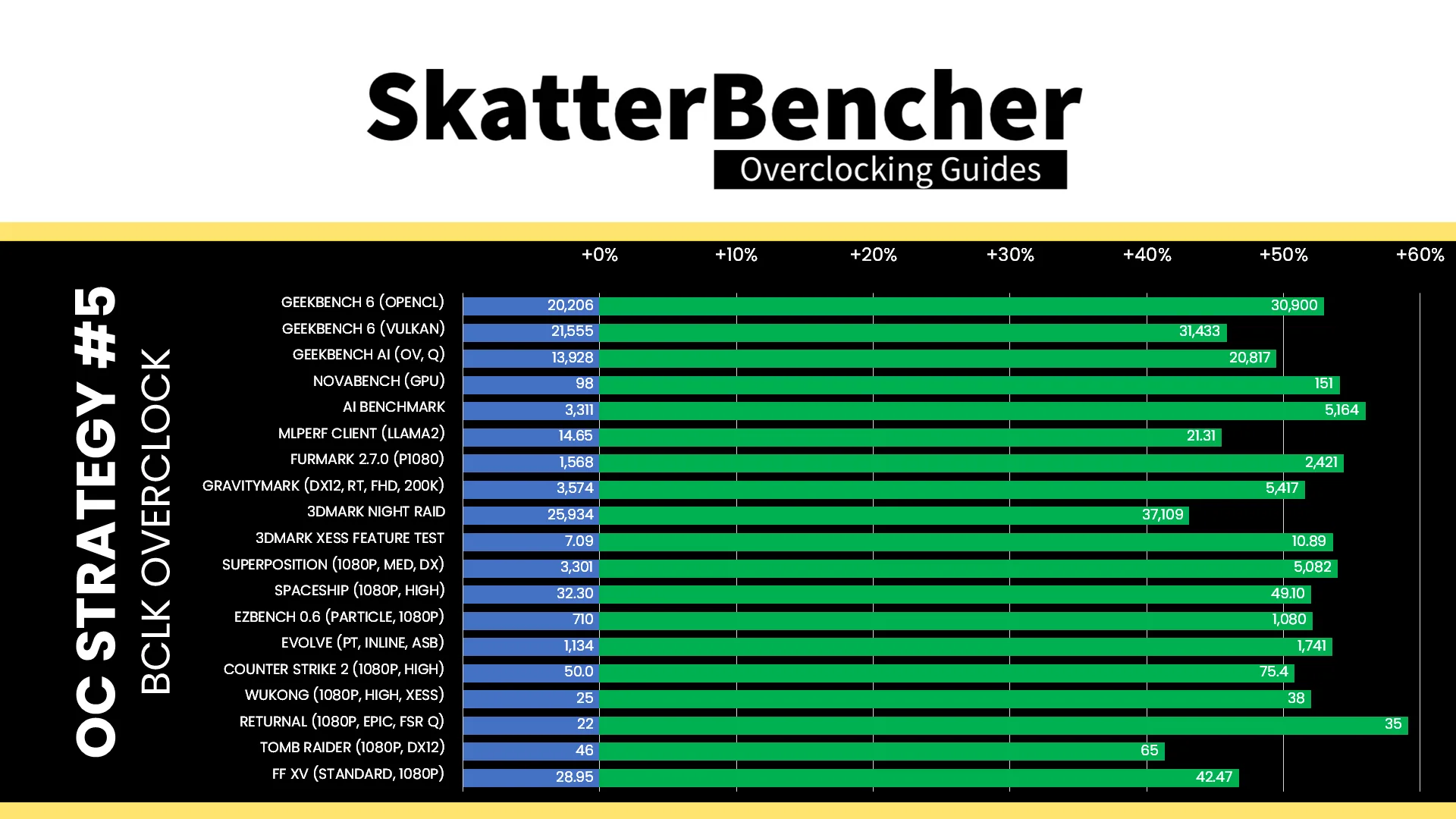
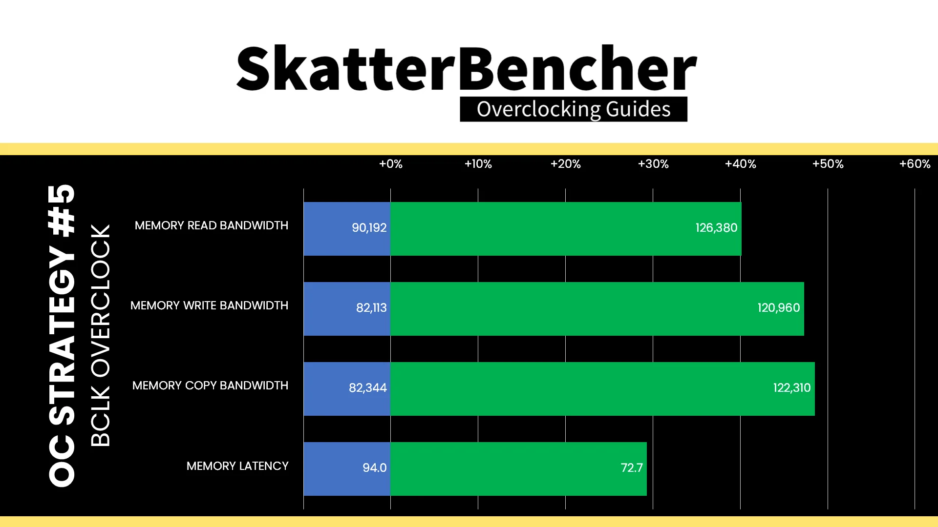
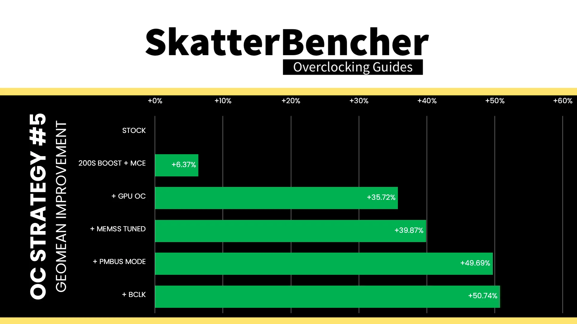
Since we’re running slightly lower frequencies than in OC Strategy #4, I didn’t expect a performance improvement. However, it seems that the performance is slightly better across the board. This suggests that perhaps the GFX-D2D is indeed affected by the SoC reference clock, or some part of the memory subsystem is more efficient. The Geomean performance improves by slightly over one percentage point to +50.74%, and we get a maximum improvement of +59.09% in Returnal.
When running the 3DMark Speed Way Stability Test, the average GPU clock is 3055 MHz with 1.249 volts. The GPU memory clock is 4030 MHz. The average GPU Temperature is 40 degrees Celsius, and the average GPU Cores Power is 17.9 watts.
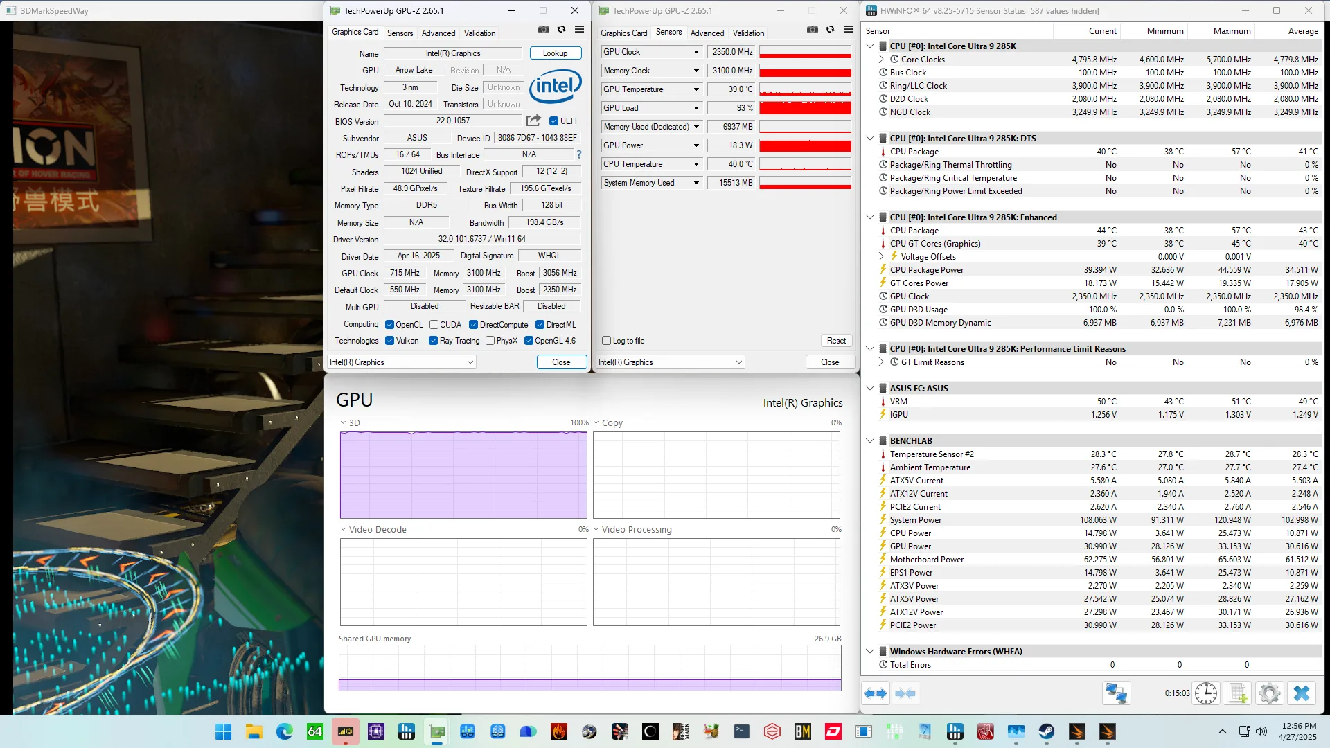
When running the OCCT 3D Standard Stress Test, the average GPU clock is 3055 MHz with 1.201 volts. The GPU memory clock is 4030 MHz. The average GPU Temperature is 50 degrees Celsius, and the average GPU Cores Power is 28.4 watts.

Intel Arrow Lake Integrated Graphics: Conclusion
Alright, let us wrap this up.
Back in October last year, I put up a blog post series on Arrow Lake overclocking which also covered the integrated graphics aspect. I looked forward to putting together a full guide since integrated graphics overclocking always gives nice performance uplifts and also requires tuning the memory subsystem. That’s no different on Arrow Lake as we get a +50% geomean performance improvement from GPU and memory overclocking.
There are a couple things that I think would improve the Intel Graphics (Arrow Lake) overclocking experience.
First of all, I’d love to see full integrated graphics overclocking support in the BIOS. That includes controls over the SVID voltage request which we currently don’t have in the ROG BIOS. This is needed to workaround the performance throttling issues because we need to set the SVID request to a low value while using PMBus mode to set the actual voltage.
I understand there’s probably not so much demand for these options, but for enthusiasts it’s always better to have the option and not need it, than to need the option and not have it.
Second, I’d love for Intel to give us more control over the clocking of the various IP blocks like the other D2Ds, the NPU, and VPU. When using BCLK overclocking these become the bottleneck since we can’t even adjust the ratio downwards.
Lastly, I do want to commend the Intel team on the BCLK implementation on Arrow Lake. The dual BCLK architecture was really helpful for IGP overclocking because asynchronous mode keeps the compute tile running at the standard 100 MHz reference clock. I know there’s been some discussion about the value of BCLK overclocking, but in this guide I (hopefully) illustrate its usefulness. Like I said: at the end of the day, it’s better to have the option and not need it than to need the option and not have it.
Anyway, that’s it for this gude.
I want to thank my Patreon supporters and YouTube members for supporting my work. If you have any questions or comments, please drop them in the comment section below.
See you next time!