Arrow Lake Ring Overclocking
We have a closer look at tuning the performance of the the Arrow Lake Ring data fabric, located on the Compute Tile.
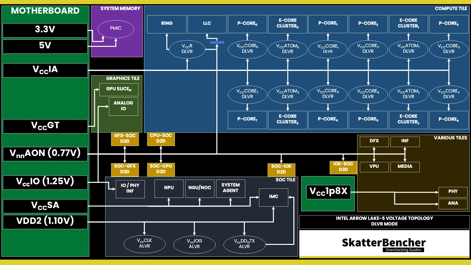
Arrow Lake is Intel’s revolutionary new processor for mainstream desktop, featuring new P-cores and E-cores, disaggregated tile-based 3D Foveros packaging, an integrated NPU for AI acceleration, a next-generation uncore, DLVR power rails, and so much more.
In this blog post series, I have a closer look at Arrow Lake and explore its performance tuning and overclocking opportunities. I will cover the Compute (P-core, E-core, Graphics, NPU), Memory Subsystem (DDR, MC), and Data Fabric (Ring, NGU, D2D).
Arrow Lake Ring: Introduction
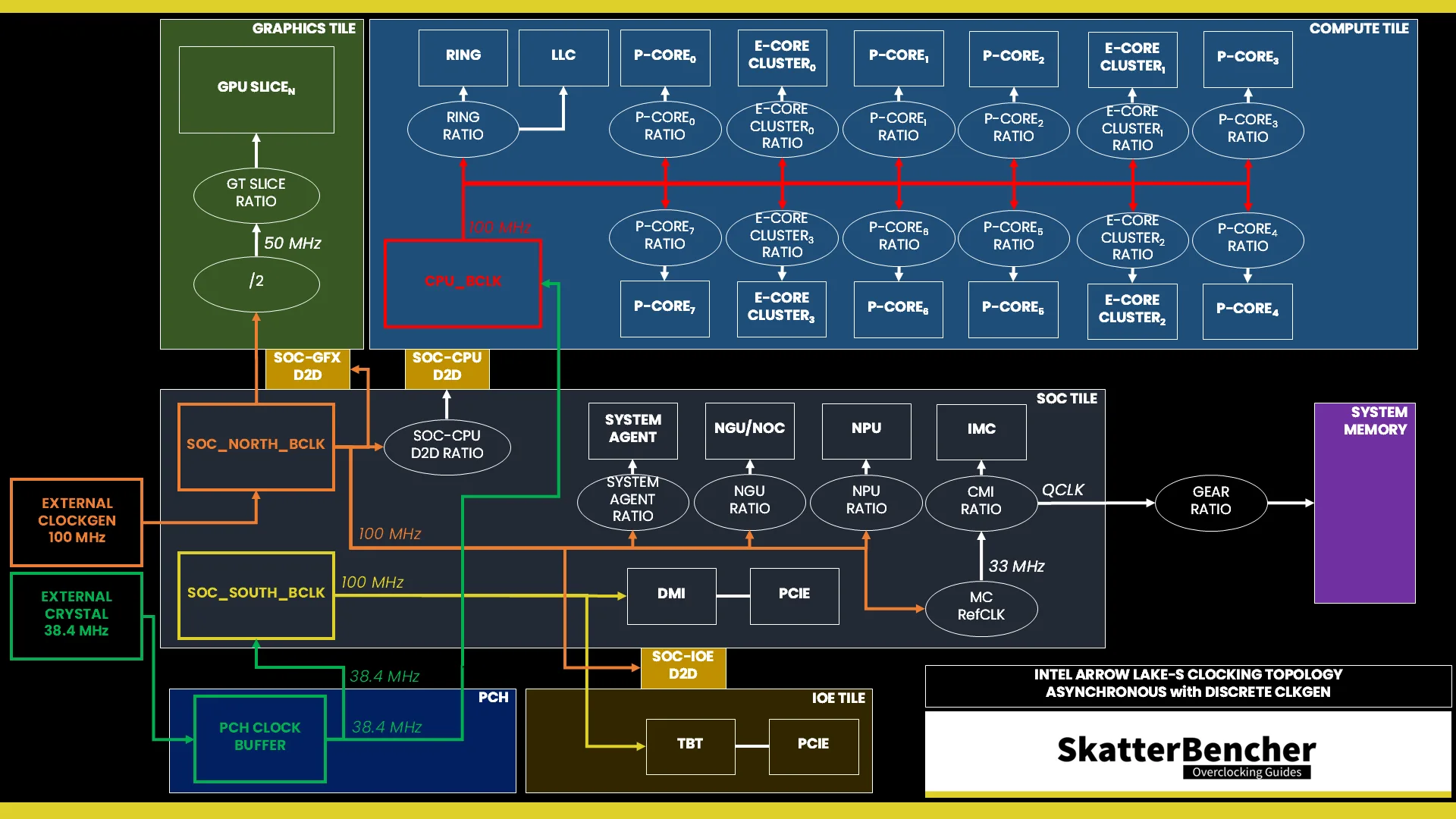
The Ring fabric provides the data fabric interface between the various Compute IP blocks in the Compute Tile, the last-level cache, and the SOC-Compute D2D interface.

Arrow Lake Ring: Clocking
The clocking of the Ring is similar to previous architectures: a reference clock is multiplied with a Ring ratio to achieve the eventual operating frequency.


Reference Clock
The 100 MHz reference clock frequency is generated internally by the CPU PLL. This clock affects all IP blocks in the Compute Tile, including the P-cores, E-cores, and Ring. This PLL can be linked to the SoC PLL when you run in synchronous mode or work independently if you run asynchronous mode.
You can configure the CPU BCLK frequency between 40 and 1000 MHz.
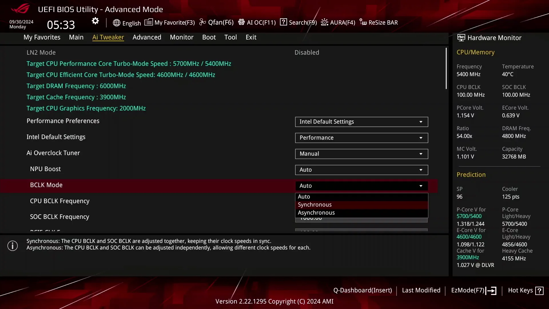
In the ASUS ROG BIOS, you can configure the CPU BCLK Frequency in the Ai Tweaker menu by first setting the Ai Overclock Tuner to anything else than Auto.

You can switch between Asynchronous and Synchronous mode by adjusting the BCLK mode option.
Ring Ratio
The reference clock is multiplied by the Ring ratio to achieve the final clock frequency. It operates independently from the P-cores and the E-cores. The Ring Ratio Limit starts from 8X. The default ratio is 39X, which yields a 3.9 GHz operating frequency. The maximum configurable ratio is 85X.
In the ASUS ROG BIOS, you can configure the minimum and maximum Ring Ratio in the Ai Tweaker main menu.

It’s important to note that the Ring frequency cannot exceed the maximum P-core or E-core frequency. So even if the maximum Ring ratio is set to 39X, if all P-cores and E-cores are limited to 38X, then the Ring will also be limited to 38X.
Ring Downbin
Intel Ring Downbin, or Ring to Core Ratio Offset, is a legacy power management feature that reduces the Ring ratio compared to the Core ratio. It is no longer enabled by default on Arrow Lake processors, but you can still enable the feature in the BIOS.
The Ring Downbin dynamically adjusts the Ring frequency based on the P-core and E-core frequency. By default, the Ring frequency will always run at its maximum allowed frequency. That’s the lower of the configured maximum Ring Ratio and current P-core and E-core ratios.
In the ASUS ROG BIOS, you can enable Ring Downbin in the Ai Tweaker main menu.

Arrow Lake Ring: Voltage
The voltage regulation for the Ring is more complex than prior generations of Intel Core processors due to the introduction of the DLVR. The DLVR enables much lower voltage levels for the Ring but still relies on a dynamic external motherboard voltage regulator as the input voltage source.

V/F Curve
The Core Ultra 9 285K Ring has its own V/F curve which is defined by up to nine (9) V/F points. The first eight (8) V/F points are factory-fused and the last point is mapped to the “OC Ratio.”

Here is the Ring’s V/F curve for my specific Core Ultra 9 285K. The voltage is 0.826V between 8X and 34X, then increases to 1.054V for VF Point 6 at 3.8 GHz, and 1.106V for VF Point 7 at 3.9 GHz.

3.9 GHz is the default maximum frequency for the Ring. However, there’s an eighth factory-fused V/F Point at 1.159V for 4 GHz too. This point gets “unlocked” when you also program an “OC Ratio.”
Unfortunately, the Ring V/F Points are not available in the ASUS ROG BIOS. However, you can access it using the Shamino work tool.
Advanced Voltage Offset (VF Points)
Advanced voltage offset is available for the Ring. There are nine (9) available VF Points, eight of which are fixed to a specific ratio. The final VF Point is mapped to the “OC Ratio” which, in theory, can be configured independently. However, in the ASUS BIOS, it will be set to the maximum Ring Ratio configured in the BIOS.

You can set a voltage offset for each of these V/F points. The final OC ratio’s base voltage will be the manual set adaptive voltage.
So, to clarify: in theory, you can define three ratios for the Ring: the “OC Ratio” for V/F Point 9, the minimum Ring ratio, and the maximum Ring ratio. The “OC Ratio” will ultimately define the shape of the Ring V/F curve, whereas the minimum and maximum Ring Ratio determine the allowable clock range for the Ring.

Unfortunately, the Ring V/F Points are not available in the ASUS ROG BIOS. However, you can access it using the Shamino work tool.
Voltage Limits
To safeguard the processor, Intel has imposed strict voltage limits for several IP blocks, including the Ring. This limit effectively prevents the Ring from requesting a higher voltage from the PCU.
By default, the voltage limit for the Ring is 1.356V, but this can be increased to 1.450V under ambient conditions. When the temperature is below 10 degrees Celsius, you can further increase the voltage limit or disable the limit altogether.
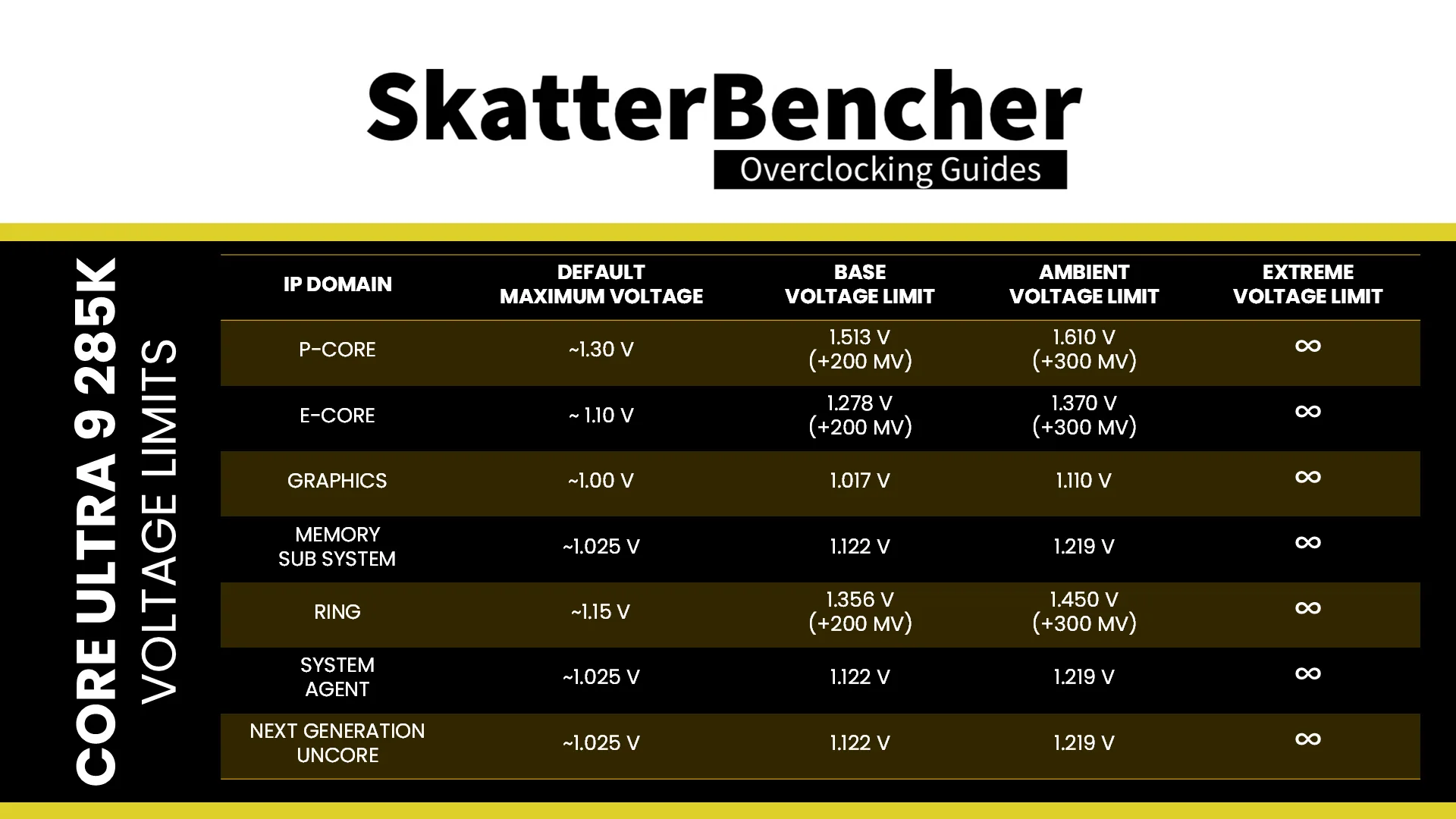
For DLVR-powered IP blocks like the Ring, in theory, you can also change to Power Gate mode to override the voltage limit and set any voltage you want. Of course, motherboard vendors can implement their own voltage limits for the voltage regulator.
In the ASUS ROG BIOS, you can configure the Ring DLVR Voltage Limit via the Ai Tweaker Max Voltage Limits sub-menu.

VccIA MBVR
The external VccIA MBVR voltage rail provides the input voltage for the individual P-core, E-core clusters, Ring, last-level cache (LLC), and E-core L2 cache. Each P-core, E-core cluster, and Ring has an individual Digital Linear Voltage Regulator (DLVR) between the VccIA rail and the IP blocks. That means each of the blocks can operate at its own voltage.
- VccCOREn is the DLVR powering an individual P-core.
- VccR is the DLVR powering the Ring and Last-Level Cache.
- VccATOMn is the DLVR powering an individual E-core cluster, which consists of four E-cores, and its L2 cache.
The DLVRs can also be bypassed. In that case, the IP blocks are running in so-called Power Gate (PG) mode. In PG mode, the VccIA voltage rail directly powers the IP blocks and they all share the same voltage. That’s similar to how previous generation desktop architectures worked.
The default mode of operation is DLVR mode. Let’s explore that first.
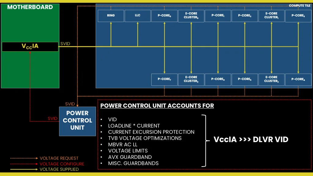
VccR DLVR Mode
Based on its VF curve, the Ring requests an operating voltage using the SVID protocol from the CPU Power Control Unit (PCU).

The PCU in turn configures the VccIA voltage rail and the VccR DLVR. There are two ways to configure the Ring voltage:
- Adaptive mode is the standard mode of operation, which relies on the factory-fused voltage-frequency curves we discussed before.
- Override mode specifies a single static voltage across all ratios. It is mainly used for extreme overclocking where stability at high frequencies is the only consideration.
We can configure override and adaptive modes directly in the PCU by specifying a target voltage and a voltage offset for each mode.

In adaptive mode, the target voltage is mapped to the Ring’s “OC Ratio.” This also matches the Ring VF Point 9. You can configure the adaptive voltage and OC Ratio to any value, however multiple rules enforce what ratio and voltage are actually set.
Rule #1: the voltage set for a given VF Point n must be higher than or equal to the voltage set for VF Point n-1.
In the case of the Ring, it means that the voltage for the OC Ratio must be higher than or equal to the voltage for VF Point 8. This can be a little strange because you can program the OC ratio to any value, including lower than 40X.
For example, let’s say you set the maximum ring ratio to 28X and the adaptive voltage to 1V. In that case, VF Point 9 will be programmed to 28X at 1V. However, the actual frequency will be 2.8 GHz with 1.159V as that’s the voltage for VF Point 8.

Rule #2: for ratios between the OC Ratio and the next highest factory-fused V/f point, the voltage is interpolated between the set adaptive voltage and the factory-fused voltage.
Let’s say we configure the Ring VF OC Point to 45X and 1.35V. The target voltage for Ring ratios between 40X and 45X is now interpolated between the factory-fused voltage for 40X and the set adaptive voltage for 45X.
One last thing about the adaptive mode. The adaptive offset is applied across the entire curve. So, if we set +100 mV adaptive offset, the operating voltage for all frequencies between 8X and the OC ratio will be increased by 100 mV.

In the ASUS ROG BIOS, you can configure the Ring DLVR Voltage in the Ai Tweaker menu. You can configure it in adaptive, manual, and offset mode.

VccIA Power Gate SVID Mode
In Power Gate Mode, all the DLVRs tied to the VccIA voltage rail are bypassed and the connected IP blocks are powered directly by the VccIA voltage rail. That includes the P-cores, E-core clusters and their cache, the Ring, and the last-level cache.
Power Gate mode is basically how the VccIA rail worked on previous generation Raptor Lake processors. For Arrow Lake, it works well … but it’s a little complicated.
To make a long story short: when the P-cores, E-cores, and Ring requests their voltage to the CPU PCU, they account for a ton of other compensations including voltage droop, DLVR efficiency, AVX Guardband, Thermal Velocity Boost voltage optimizations, and so on. The result is that the actual voltage provided from the VccIA voltage rail to the DLVRs is relatively high!
For example, here are the voltages with the CPU at stock voltage and frequency (P53X, E46X, R39X) running a light all-core workload:

We can interpret this as follows: the P-core, E-core, and Ring request a voltage to the PCU to ensure it’s running 1.15V, 1.05V, and 1.1V respectively. The PCU then adds compensation for the loadlines, CEP, TVB, AVX, AC LL, DLVR efficiency losses, and so on. At the end of the calculation, the PCU determines the VccIA voltage rail should provide 1.43V input voltage to the DLVRs.
If we were to switch to Power Gate mode but maintain the same mechanism for calculating the required voltage, then the VccIA voltage rail would effectively provide 1.43V to the P-cores, E-cores, and Ring. That’s obviously way too high for the target frequency and would quickly result in an overheating system. But this would be how voltage was configured on the previous generation Raptor Lake processor.
VccIA Power Gate PMBus Mode
Fortunately, there’s another way to approach Power Gate Mode voltage configuration: ignore the SVID voltage requests and calculations, and program the VccIA voltage regulator directly over PMBus. This process effectively allows us to take full control over the voltage set by the VccIA voltage rail.
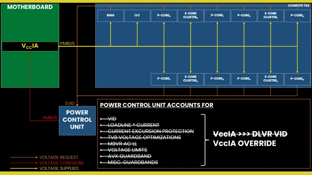
This approach is a very traditional way of overclocking whereby you set a fixed output voltage and then use an appropriate VRM loadline setting to reduce the operating voltage in higher load scenarios.
Let’s have a look at an example and compare Power Gate and DLVR in Cinebench R23.
If we set 1.35V with LLC=6, then the effective voltage under load is 1.26V. That’s about 150mV higher than with DLVR. Despite the higher voltage, the temperature is only 7C higher than when we ran DLVR.
If we set 1.30V with LLC=4, then the effective voltage under load is 1.15V which is very similar to DLVR. Despite the almost identical voltage, the temperature is 7 degrees Celsius lower than with DLVR.
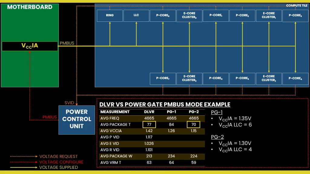
The bottom line on DLVR versus PG mode is that DLVR seems to provide better temperatures and efficiency in low-load scenarios because it can have the Ring run at lower voltage. However, in high-load scenarios where the total current exceeds 150A, the power loss translates into a not-insignificant increase in temperature, which eats into the thermal budget of our thermal solution and, ultimately, lowers the overclocking headroom.
How much exactly? Well, the power loss across a linear voltage regulator equals the decrease in voltage across the DLVR multiplied by the total load.
In our example, with a voltage drop of 305mV and 160A load, the power loss is 48.8W. Nearly all of that power loss will convert into heat.

For high-load scenarios, PG mode appears to offer better overclocking headroom because the operating temperature is lower. However, we cannot rely on the PCU to control the VccIA output voltage because its calculations are too conservative. So it ends up overvolting too much. Therefore, the right way of overclocking using PG mode is to ignore the SVID requests entirely and take direct control of the VccIA voltage regulator. This also requires setting an appropriate VR loadline to ensure lower voltage in all-core workloads.
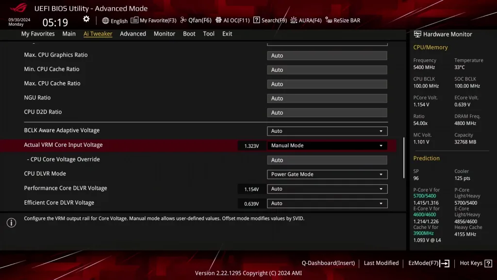
In the ASUS ROG BIOS, you can switch between DLVR and Power Gate mode for the VccIA voltage rail in the Ai Tweaker menu by configuring the CPU DLVR Mode menu item.
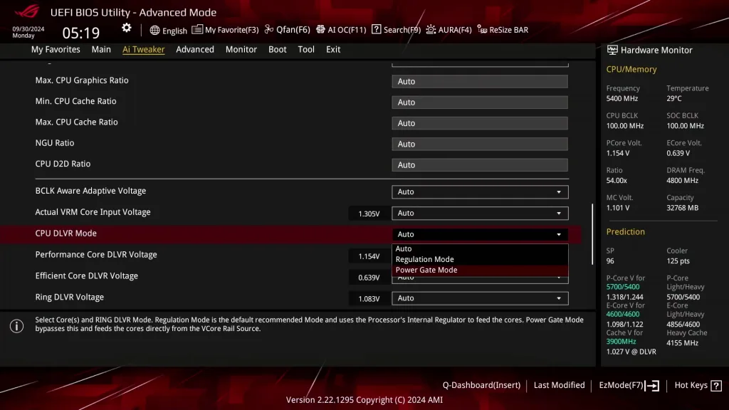
In the ASUS ROG BIOS, you can set the VccIA voltage rail in the Ai Tweaker menu by configuring the Actual VRM Core Input Voltage in manual mode.
Arrow Lake Ring: Overclock & Undervolt
The overclocking potential of the Ring is very limited. At default voltage, you can increase a couple of bins at best on the Core Ultra 9 285K to maybe 4.2 GHz. The overclocking range is a little better on the Core Ultra 5 245K due to the missing “middle P-cores”. That’s the bad news.

The good news is that Ring frequency has barely any impact on the performance. Changing from 4 GHz to 2 GHz only decreases the Cinebench R23 multi-thread performance by less than one and a half percent. So, the lack of overclocking headroom doesn’t impact the maximum performance potential.

There is significant undervolting potential, however. On my CPU, I could run the Ring at 3.9 GHz with 950 mV, which is 150 mV lower than the factory-fused V/F curve. Configuring the undervolt is a little tricky due to how the V/F Point configuration works. Therefore, I suggest you simply set a maximum Ring Ratio and an override voltage in the BIOS.

Piston_975
Hi,
where do I get the Shamino work tool? I did stir up the net, but couldn’t find anything.
I do apreciate your work, it was a great help to overclocking my Arrow Lake.
Thank you for your reply.
Kind regards
Piston_975 / Moritz from Germany
Pieter
You can find the in the ArrowLake Resources thread on the ROG forums as OCpak https://rog-forum.asus.com/t5/intel-800-series/arrowlake-resources/td-p/1051570