Arrow Lake MemSS Overclocking

We have a closer look at tuning the performance of the the Arrow Lake MemSS, or Memory Sub System, located on the SoC Tile.
Arrow Lake is Intel’s revolutionary new processor for mainstream desktop, featuring new P-cores and E-cores, disaggregated tile-based 3D Foveros packaging, an integrated NPU for AI acceleration, a next-generation uncore, DLVR power rails, and so much more.

In this blog post series, I have a closer look at Arrow Lake and explore its performance tuning and overclocking opportunities. I will cover the Compute (P-core, E-core, Graphics, NPU), Memory Subsystem (DDR, MC), and Data Fabric (Ring, NGU, D2D).
Arrow Lake MemSS: Introduction
The memory sub-system, also referred to as MemSS, consists of two DDR5 memory controllers and the system memory. The sub-system connects to the network-on-chip (NoC) which is part of the Next Generation Uncore (NGU) sub-system located on the SoC die.
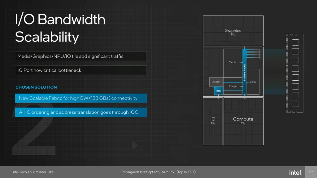
Arrow Lake has two DDR5 memory controllers, each supporting 32-bit memory channels, which are located on the SoC tile. The SoC tile is manufactured using the TSMC N6 process. The memory controller topology is slightly different on Arrow Lake than on previous DDR5 platforms as each memory controller connects to one side of the system memory DIMMs.

DDR5 overclocking isn’t very different from Raptor Lake in the sense that the general tuning principles still apply. However, there are some improvements in overclocking capability and support for CUDIMM.
By default, Arrow Lake-S supports up to DDR5-5600 memory in Gear 2 mode with UDIMM and up to DDR5-6400 in Gear 4 mode with CUDIMM.

Arrow Lake MemSS: Clocking
The clocking of the two DDR5 memory controllers is similar to previous architectures: a reference clock is multiplied with a ratio to achieve the eventual operating frequency. It is intimately tied to the system memory clock frequency.
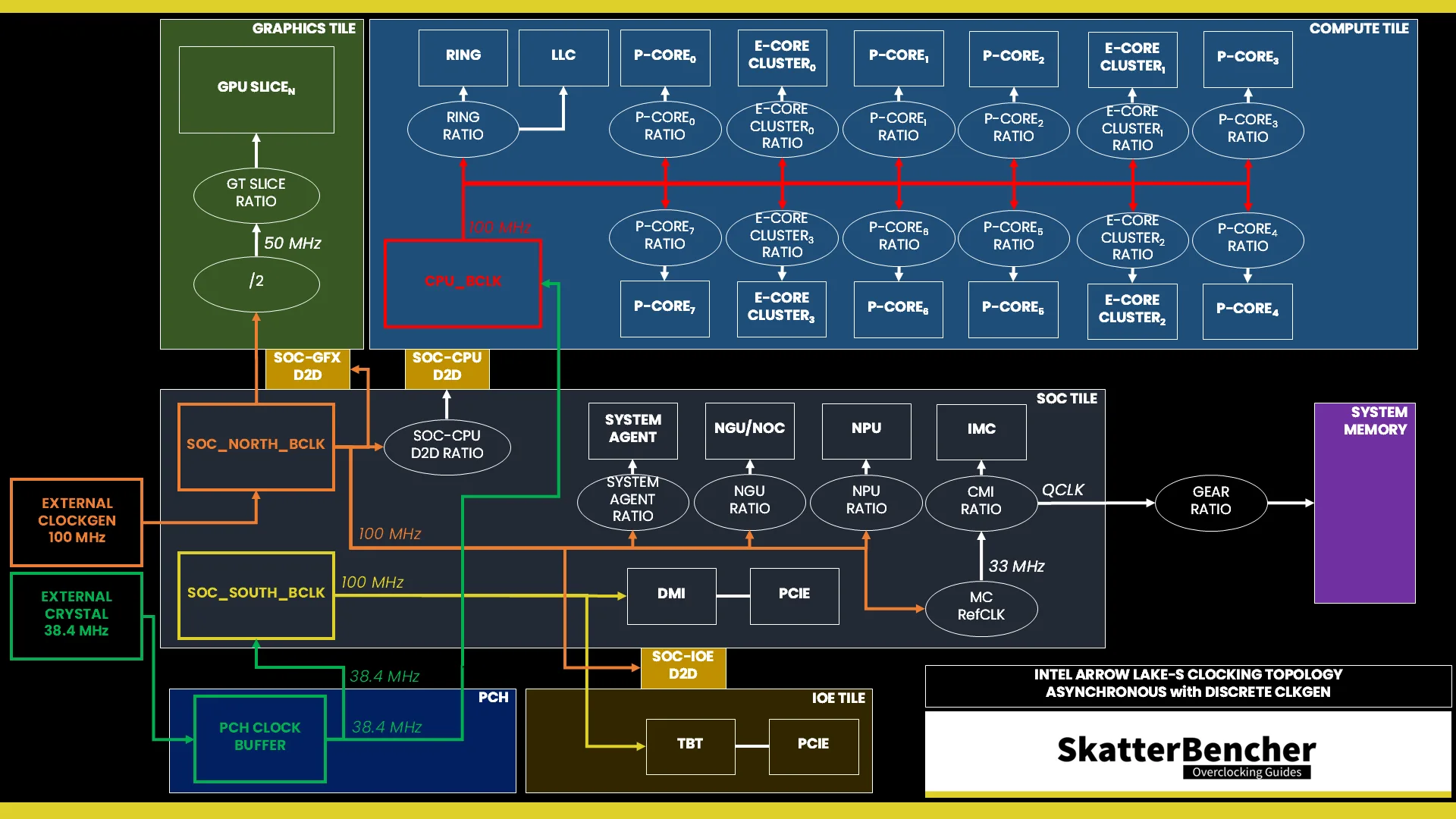
The easiest way to think about configuring the memory controller clock frequency is first to determine the system memory frequency, then set the gear ratio which divides the memory frequency either by two or by four to achieve the memory controller frequency. However, behind the scenes, the configuration is the other way around.
Reference Clock
The 100MHz reference clock is derived internally from the SoC PLL. However, it can also be clocked with an external clock generator providing the reference clock for the SoC Tile. This clock affects nearly all the IP blocks of Arrow Lake, except for those in the Compute Tile and the PCIe/DMI links. This PLL can be linked to the CPU PLL when you run in synchronous mode or work independently if you run asynchronous mode.
You can configure the SOC BCLK frequency between 40 and 1000 MHz. This 100 MHz reference clock is then multiplied by 4, and divided by 2, 3, 4, 6, or 12 to achieve a reference clock of 33, 66, 100, 133, or 200 MHz. Let’s call this the Memory Controller Reference Clock (MCRefCLK).
In the ASUS ROG BIOS, you can configure the SOC BCLK Frequency in the Ai Tweaker menu by first setting the Ai Overclock Tuner to anything else than Auto.
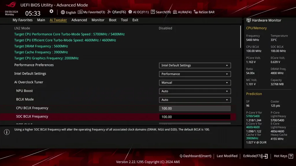
You can switch between Asynchronous and Synchronous mode by adjusting the BCLK mode option.

CMI Ratio
The MCRefCLK is then multiplied by a “CMI ratio” (Convergent Memory Interface) to achieve the final Memory Controller frequency (QCLK). The system memory operating frequency, defined as the DCLK, is then obtained by multiplying the QCLK by 2 times the “Gear Type + 1”. The memory data rate (in MT/s) is twice the memory frequency due to the “double data rate” technology.
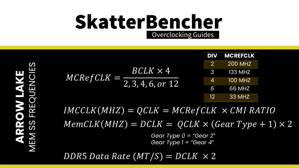
There are two Gear Types available for Arrow Lake. Gear Type 0 is better known as “Gear 2” and Gear Type 1 is known as “Gear 4”.
In the ASUS ROG BIOS, you can configure Gear Type via the Ai Tweaker menu by adjusting the Memory Controller : DRAM Frequency Ratio.

Let’s look at an example:
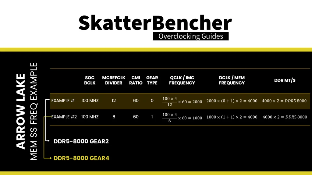
In the first example, we use an MCRefClk of 33 MHz, Gear 2, and a CMI Ratio of 60. That gives us a Memory Controller frequency of 2 GHz, a memory frequency of 4GHz, and DDR5-8000 data rate. In the second example, we change the Refclk divider to 6 and use Gear 4. Now, we still have DDR5-8000 system memory but the Memory Controller is running at 1 GHz instead.
In practice, configuring the memory subsystem frequencies is much more simplified as we can simply select a system memory data rate (e.g. DDR5-8000) and select Gear 2 or Gear 4. The MCRefClk and CMI Ratio are automatically determined by the BIOS auto-rules. The Memory Ratio starts from DDR5-800 and goes up to DDR5-15066 in the ASUS BIOS, but should in theory go up to 34 GT/s.
In the ASUS ROG BIOS, you can configure memory frequency via the Ai Tweaker menu by adjusting the DRAM Frequency option.

Arrow Lake MemSS: Voltage
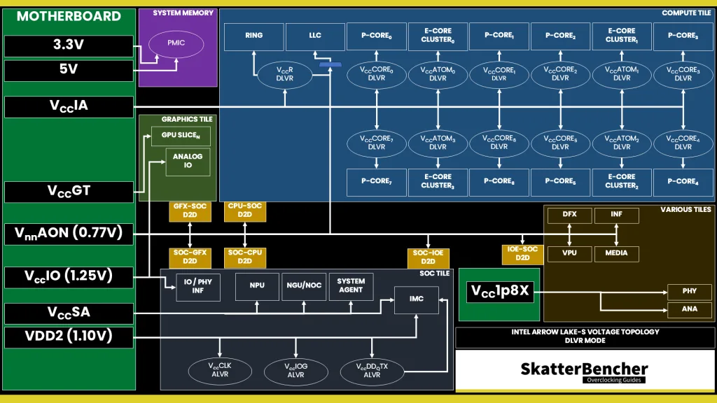
Two important voltage rails are driving the overclocking capabilities of the memory controller: VccSA for the digital portion and VDD2 for the analog portion.
V/F Curve
The MemSS has its own V/F curve which is defined by up to four (4) V/F points. Each V/F Point is defined by a CMI ratio, a Gear Type, and a VccSA interpolated voltage. As far as I understand, these points are all individually definable, but unfortunately, I couldn’t quite work out how to do it.
Unfortunately, the MemSS V/F Points are not available in the ASUS ROG BIOS. However, you can access it using the Shamino work tool.
VccSA MBVR
The external VccSA MBVR powers several parts of the SOC dielet, including the memory controller. Unlike the Compute tile, the parts of the SOC dielet are not powered using DLVR. So, the power delivery is identical to previous architectures.
The most relevant parts powered by the VccSA voltage rail are the neural processor, the next-generation uncore, and the memory controller. The voltage configuration of the VccSA voltage rail is rather complicated. Since multiple IP domains share the voltage rail, the VccSA voltage is set based on the highest requested voltage from the various connected IP blocks.
VccSA Power Gate SVID Mode
Given the MemSS has its own V/F curve, it can dynamically request an operating voltage from the VccSA voltage rail using the SVID protocol. The voltage configuration is adaptive in the sense that each of the four defined V/F Points can have its own target voltage. The ultimate VccSA voltage is defined by the maximum voltage request from all VccSA-powered rails, including the NGU and the MemSS.

Having the MemSS capable of overriding the VccSA voltage is useful primarily in situations where a dynamic memory frequency technology is enabled. In that case, the memory controller needs to train each V/F point at boot and higher memory frequencies may require higher VccSA voltages. However, as an end-user, we rarely interact with this part of the system configuration.
Unfortunately, the MemSS adaptive mode voltage configuration is not available in the ASUS ROG BIOS.
VccSA Power Gate PMBus Mode
As mentioned, the MemSS adaptive voltage SVID mode is not available in the ASUS BIOS. However, that doesn’t mean we can’t configure the voltage as there’s a second way to approach Power Gate Mode voltage configuration: ignore the SVID voltage requests and calculations, and program the VccSA voltage regulator directly over PMBus. This process effectively allows us to take full control over the voltage set by the VccSA voltage rail.

This approach is a very traditional way of overclocking whereby you set a fixed output voltage and then use an appropriate VRM loadline setting – if available – to reduce the operating voltage in higher load scenarios. The loadline configuration isn’t particularly useful for SA voltage rail.
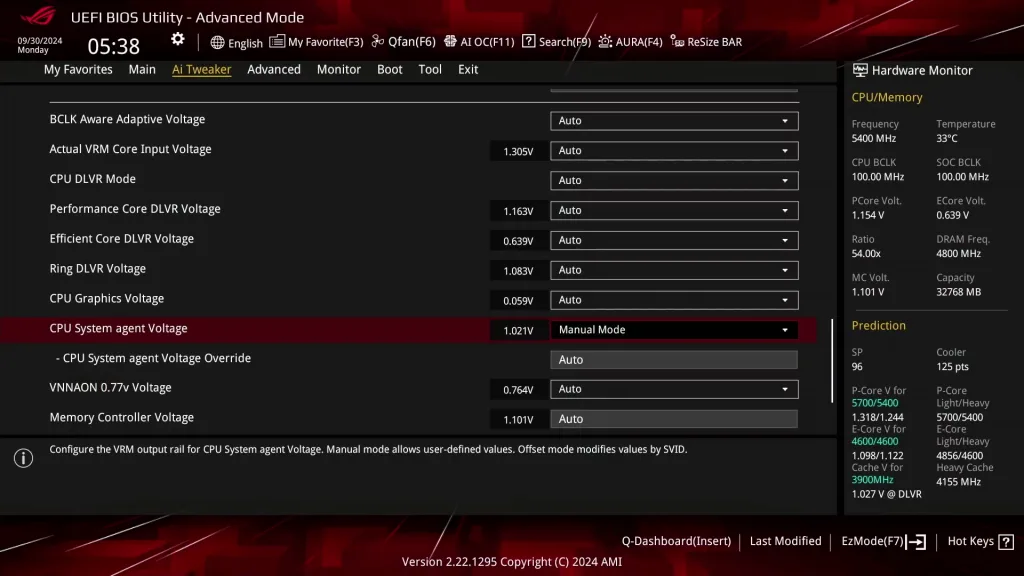
In the ASUS ROG BIOS, you can configure the VccSA voltage rail in the Ai Tweaker menu by configuring the CPU System Agent Voltage in manual mode.
Voltage Limits
To safeguard the processor, Intel has imposed strict voltage limits for several IP blocks, including the MemSS. This limit effectively prevents the MemSS from requesting higher voltage from the VccSA voltage rail.
By default, the voltage limit for the MemSS is 1.122V, but this can be increased to 1.219V under ambient conditions. When the temperature is below 10 degrees Celsius, you can further increase the voltage limit or disable the limit altogether.
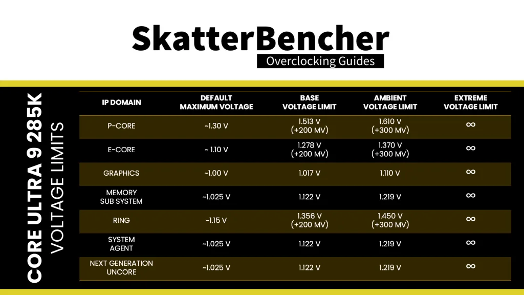
Unfortunately, you cannot set the MemSS voltage limit independently in the ASUS ROG BIOS.
For the VccSA-powered IP blocks like the MemSS, you can also disable SVID communication between the IP domain and the voltage regulator. In that case, the voltage limit no longer restricts the maximum voltage.
VDD2 MBVR
The external VDD2 MBVR is a static 1.1V rail that powers several parts on the SOC, including the VDDQTX and Analog IO part of the DDR PHY. It is also referred to as the Memory Controller Voltage in the ASUS BIOS.
In the ASUS ROG BIOS, you can set the VDD2 voltage rail in the Ai Tweaker menu by configuring the Memory Controller Voltage.

VDDQTX ALVR
The internal VDDQTX analog linear voltage rail powers the transmission signaling from the memory controller to the system memory. On the ASUS motherboards, it is by default in bypass mode and synchronized with the VDD2 voltage.
In the ASUS ROG BIOS, you can configure the VDDQTX voltage rail in the Ai Tweaker Advanced Memory Voltages submenu by adjusting the VccDdqControl Bypass option. You can manually set the voltage in the same menu using the Vddq Voltage Override option.

VccIO MBVR
The external VccIO MBVR is a static 1.25V rail that powers many of the analog IO like USB3 and Display. Unlike prior generations, it has nothing to do with the memory controller or memory overclocking.
In the ASUS ROG BIOS, you can set the VccIO voltage rail in the Ai Tweaker Tweaker’s Paradise sub-menu by configuring the VccIO 1.25v Voltage option.

DDR PMIC
The on-package DRAM Power Management Integrated Circuit (PMIC) is the primary source of power for the DDR5 modules.

On Arrow Lake, the DDR5 PMIC has two input voltages: 5V and 3.3V. The spec further defines 4 switching output regulators for 2 times VDD, VDDQ, and VPP, and 2 LDO outputs of 1.8V and 1.0V.
- VDD is 1.1V for the DRAM cell voltage
- VDDQ is 1.1V for the DRAM IO supply
- VPP is 1.8V for the DRAM wordline voltage
The PMIC also has plenty of other features such as I2C and I3C, over-voltage and over-temperature protection, and so on. As every DDR5 DIMM has its own PMIC, you can run separate voltages on the sticks.
In the ASUS ROG BIOS, you can access the PMIC settings in the Ai Tweaker Advanced Memory Voltages submenu. You can change the settings of all PMICs in sync or change the settings of each PMIC individually.

Note that there are two types of PMICs: secure and non-secure.
The main difference is that secure PMICs support voltages up to 1.435V in steps of 5mV and non-secure PMICs support voltages up to 2.070V in steps of 10mV. This granularity is important for extreme overclockers who are looking to push the memory frequency to the limit.
In the ASUS ROG BIOS, you can enable high-voltage mode in the Ai Tweaker menu by adjusting the High DRAM Voltage Mode menu item.

Arrow Lake MemSS: Overclock
Overclocking the memory subsystem is not substantially different from previous-generation platforms. For fine-tuning performance, you have a near-unlimited number of knobs and dials that control the memory frequency, timings, signaling parameters, and training methods.
Memory sub-system performance optimization is pretty much a black art that only a few people in the world truly master. At the root of the tuning is trying settings one by one to see if they make an impact on performance.
I won’t dig into the details of memory optimization as that’s a computer science university course on its own. However, I can provide some guidelines on how to approach the optimization process from a casual overclocker’s perspective.
Intel XMP 3.0
Intel Extreme Memory Profile 3.0 is the new XMP standard for DDR5 memory and is the successor to XMP 2.0 for DDR4 memory. It was introduced together with the Alder Lake processors in 2021. It is largely based on the XMP 2.0 standard but has additional functionality.

The XMP 3.0 standard is designed with six sections. One global section describes the generic data that is used across the profiles. The other five sections are designed for five profiles respectively.
- Profile 1 is meant for the performance profile (this is the standard XMP as we know it)
- Profile 2 is designed for the extreme settings (this could be a higher frequency at higher voltage)
- Profile 3 is designed for the fastest settings (this could be tighter timings at higher voltage)
- Profiles 4 and 5 are rewritable and meant for user custom settings
Each profile has a wide range of configurable fields related to voltage, frequency, and memory timings, including:
- Voltage: Module VPP, VDD, VDDQ, Memory Controller Voltage
- Primary Timings: tCL, tRCD, tRP, tRAS, Command Rate
- Secondary Timings: tRC, tWR, tRFC1, tRFC2, tRFCsb
- Miscellaneous: Dynamic Memory Boost support, Real-Time Memory Frequency OC support, Vendor ID
In the ASUS ROG BIOS, you can access the XMP Profiles in the Ai Tweaker menu via the Ai Overclock Tuner menu item.

ASUS Memory Presets
ASUS Memory Presets is an ASUS overclocking technology that provides you with a selection of memory-tuning presets for certain memory ICs. The presets will adjust the memory timings and voltages.
On the ASUS ROG Z890 Apex motherboard (BIOS 0701) there are 3 presets available for Hynix 2x16GB and 2x24GB A-die memory. However, I’m sure future BIOSes will introduce more profiles.
In the ASUS ROG BIOS, you can access the Memory Presets in the Ai Tweaker DRAM Timing Control Memory Presets submenu.

ASUS DRAM Clock Period
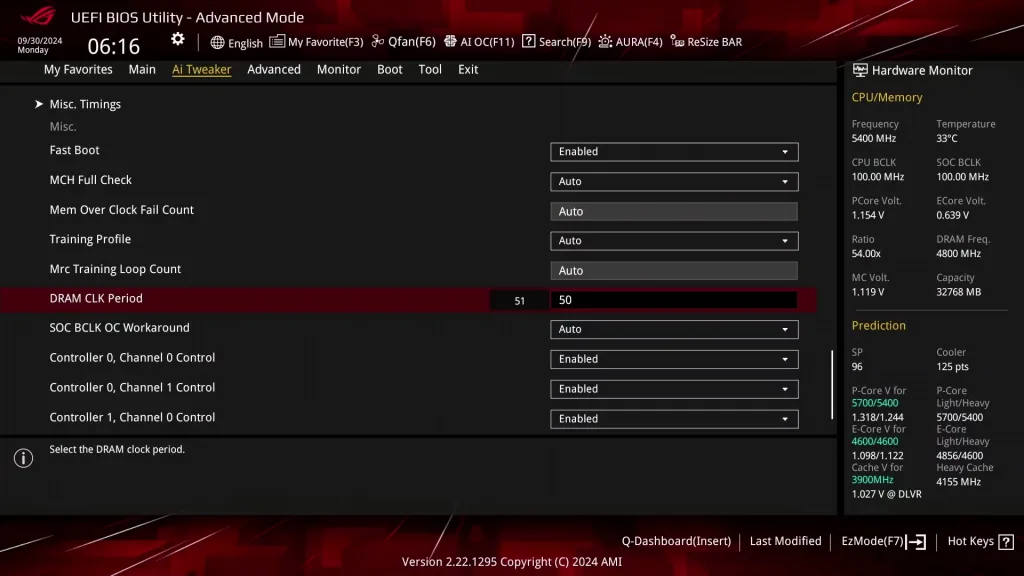
DRAM Clock Period is an ASUS-specific memory configuration option that lets you train the system memory as if it were running at a different frequency. For example, you can train DDR5-8400 memory as if it were DDR5-6000 memory.
The main advantage is that the memory controller will use more aggressive memory timings associated with lower-speed memory. After training with the aggressive timings, then the memory frequency is increased to the target frequency.
The DRAM CLK Period options refer to the DRAM Frequency menu item in the Ai Tweaker main menu. The reference number matches the current memory frequency. Setting lower lets you train as lower memory frequencies. Note that the memory frequency list in the Ai Tweaker main menu doesn’t list all available memory ratios, so it’s not easy to find the exact one-to-one mapping. So it’s really a matter of trial and error to find the lowest stable value.
In the ASUS ROG BIOS, you can access the DRAM CLK Period in the Ai Tweaker DRAM Timing Control submenu.
ASUS DIMM Fit
DIMM FIT is a brand-new ASUS overclocking technology that provides you with a means to finetune the memory signaling quality for your specific processor, motherboard, and system memory. The main goal is to improve the signaling and therefore expand overclocking headroom or improve memory stability.

The DIMM Fit process performs a grid search for the optimal hyperparameters for your memory. That involves several reboots and quick stability checks to analyze stability with various parameters. Therefore, it’s required that your system is at least somewhat stable to go through this process.
The best way to utilize this technology is to first find a stable memory configuration, then run DIMM fit, and afterward try higher frequencies. You can also use it to achieve superior stability. For example, increasing the memtest stability from half an hour to several hours.
In the ASUS ROG BIOS, you can access the DIMM Fit feature in the Ai Tweaker DRAM Timing Control submenu.

Intel Dynamic Memory Boost
Dynamic Memory Boost is an Intel technology that enables at-runtime switching between two memory profiles: the standard JEDEC SPD profile and the selected Intel XMP 3.0 profile. The dynamic switching is based on the workload demands.

In the ASUS ROG BIOS, you can enable Dynamic Memory Boost in the Ai Tweaker DRAM Timing Control Configure Memory Dynamic Frequency Switching submenu.

Intel Realtime Memory Frequency
Realtime Memory Frequency is another Intel technology that enables at-runtime switching between two memory profiles, also between the default JEDEC SPD profile and an Intel XMP 3.0 profile.
I’m not quite sure what’s the difference between Dynamic Memory Boost and Realtime Memory Frequency. But it seems they are mutually exclusive technologies.
In the ASUS ROG BIOS, you can enable Realtime Memory Frequency in the Ai Tweaker DRAM Timing Control Configure Memory Dynamic Frequency Switching submenu.

Arrow Lake MemSS: Overclocking Performance
I find that optimizing the memory frequency and timings can have a sizeable impact on AIDA64 and benchmark performance.
By enabling the DDR5-8400 XMP profile, the bandwidth increases by more than 50%, and the latency improves by 25%. Further memory subsystem performance optimization with tweaked sub-timings, increased NGU and D2D operating frequencies, and adjusted DRAM Clock Period, yields another 30 percentage points additional bandwidth and doubles the improvement in memory latency.

Adjusting the memory controller frequency from Gear 2 to Gear 4 doesn’t have that much of an impact on the memory bandwidth. However, it severely impacts the memory latency.

At DDR5-4800 with Gear 2, the memory bandwidth is about 70 GB/s with 100ns latency. With Gear 4, the memory bandwidth is still approximately 70 GB/s but the latency drastically increased to 127ns. We see the same at DDR5-8400 when enabling XMP: the memory bandwidth is about the same between Gear 2 and Gear 4, however the latency is much worse.

I could use Gear 2 mode up to DDR5-8600 without much tuning, meaning the memory controller ran at 4.3 GHz.

It’s hard to say what to expect in terms of memory overclocking since it depends a lot on the motherboard, processor, and memory kit. However, I believe these are somewhat the upper limits with ambient cooling.
| Memory Configuration | Gear Type | Memory Frequency |
| 2×16 GB | Gear 2 | DDR5-8400 |
| 2x 16GB | Gear 4 | >DDR5-9000 |
| 2x 24 GB | Gear 2 | DDR5-9000 |
| 2x 24 GB | Gear 4 | >DDR5-10000 |