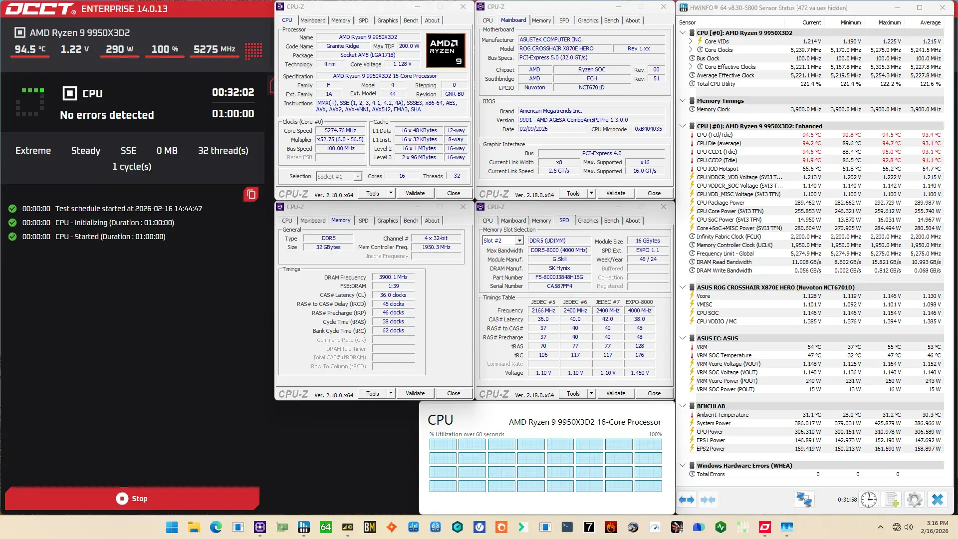
SkatterBencher #100: Ryzen 9 9950X3D2 Overclocked to 5860 MHz

Today we undervolt and overclock the AMD Ryzen 9 9950X3D2 processor up to 5860 MHz with the ASUS ROG Crosshair X870E hero motherboard.
I do this by leveraging Precision Boost Overdrive tools like Fmax Boost Override, Curve Optimizer, but also delve into memory subsystem tuning, asynchronous eCLK, and OC Mode. In this guide, I break down the Ryzen 9 9950X3D2 tuning process into five unique overclocking strategies for beginner and advanced overclockers.
- First, we enable Precision Boost Overdrive 2 and EXPO,
- Second, we tune with the Precision Boost Overdrive 2 toolkit (incl. Curve Optimizer),
- Third, we tune the memory subsystem performance,
- Fourth, we use asynchronous eCLK,
- And, finally, we try two static manual overclocks.
However, before we jump into overclocking, let us quickly review the hardware and benchmarks used in this video.
AMD Ryzen 9 9950X3D2: Introduction
The AMD Ryzen 9 9950X3D2 is part of AMD’s Zen 5-based Ryzen 9000 desktop processor product line codenamed “Granite Ridge.” The Granite Ridge processors were introduced on June 2, 2024, during Computex 2024.
The 16-core Ryzen 9 9950X3D2 is the bigger brother of the Ryzen 9 9950X and Ryzen 9 9950X3D which we overclocked in SkatterBenchers #81 and #85. It’s AMD’s first dual-X3D CPU which enthusiasts have been asking for since X3D was introduced back in 2022.
The Ryzen 9 9950X3D2 has a base clock of 4.3 GHz and a listed boost frequency of up to 5.6 GHz. Its TDP is 200W.
Platform Overview
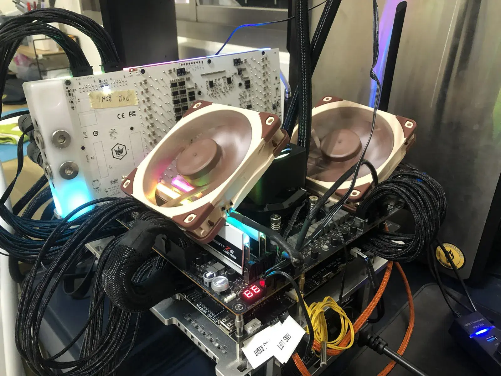
The system we’re overclocking today consists of the following hardware.
| Category | Item |
|---|---|
| CPU | AMD Ryzen 9 9950X3D2 |
| Motherboard | ASUS ROG Crosshair X870E Hero |
| CPU Cooling | Enermax LIQMAXFLO 420 |
| Memory | G.SKILL Trident Z5 Neo DDR5-8000 32GB |
| Power Supply | XPG Fusion 1600W Titanium |
| Graphics Card | GALAX GeForce RTX 4090 HOF |
| Storage | AORUS RGB NVMe M.2 512GB Gen4 AGI 512GB NVMe M.2 Gen3 |
| Chassis | Open Benchtable V2 |
| Telemetry | BENCHLAB |
Benchmarks, Games & Tools
We use Windows 11 and the following benchmark applications and games to measure performance and ensure system stability.
| Benchmark | Link |
|---|---|
| Pyprime 2.0 | https://github.com/mbntr/PYPrime-2.x |
| 7-Zip 25.01 | https://www.7-zip.org/ |
| IndigoBench Bedroom | https://www.indigorenderer.com/indigobench |
| Geekbench 6 | https://www.geekbench.com/ |
| Geekbench AI | https://www.geekbench.com/ai/ |
| Cinebench 2026.1 | https://www.maxon.net/en/cinebench/ |
| CPU-Z | https://www.cpuid.com/softwares/cpu-z.html |
| V-Ray 6 | https://www.chaosgroup.com/vray/benchmark |
| Corona 10 Benchmark | https://corona-renderer.com/benchmark |
| AI-Benchmark | https://ai-benchmark.com/ |
| LocalScore 14B | https://www.localscore.ai/ |
| Y-Cruncher 5B | http://www.numberworld.org/y-cruncher/ |
| PugetBench for Creators | https://www.pugetsystems.com/pugetbench/creators/ |
| 3DMark CPU Profile | https://www.3dmark.com/ |
| OCCT | https://www.ocbase.com/ |
| AIDA64 | https://www.aida64.com/ |
| Game | Link |
|---|---|
| Counter Strike 2 | https://store.steampowered.com/app/730/CounterStrike_2/ |
| Returnal | https://store.steampowered.com/app/1649240/Returnal/ |
| Shadow of the Tomb Raider | https://store.steampowered.com/app/750920/Shadow_of_the_Tomb_Raider_Definitive_Edition/ |
| Monster Hunter Wilds | https://www.monsterhunter.com/wilds/en-us/benchmark/ |
| Age of Mythology Retold | https://store.steampowered.com/app/1934680/Age_of_Mythology_Retold/ |
| Forza Motorsport | https://store.steampowered.com/app/2440510/Forza_Motorsport/ |
| Homeworld 3 | https://store.steampowered.com/app/1840080/Homeworld_3/ |
I use the following tools to check and log system telemetry, adjust clock frequencies, and launch benchmarks.
| Tool | Link |
|---|---|
| Benchmate | https://benchmate.org/ |
| CPU-Z | https://www.cpuid.com/softwares/cpu-z.html |
| HWiNFO | https://www.hwinfo.com/ |
| NopBench | https://skatterbencher.com/nopbench/ |
| Shamino OCPak | https://rog-forum.asus.com/t5/amd-600-series/x670-x870-resource-thread/m-p/901576/ |
| Ryzen LoopFmax | https://skatterbencher.com/ryzen-loopfmax/ |
AMD Ryzen 9 9950X3D2: Stock Performance
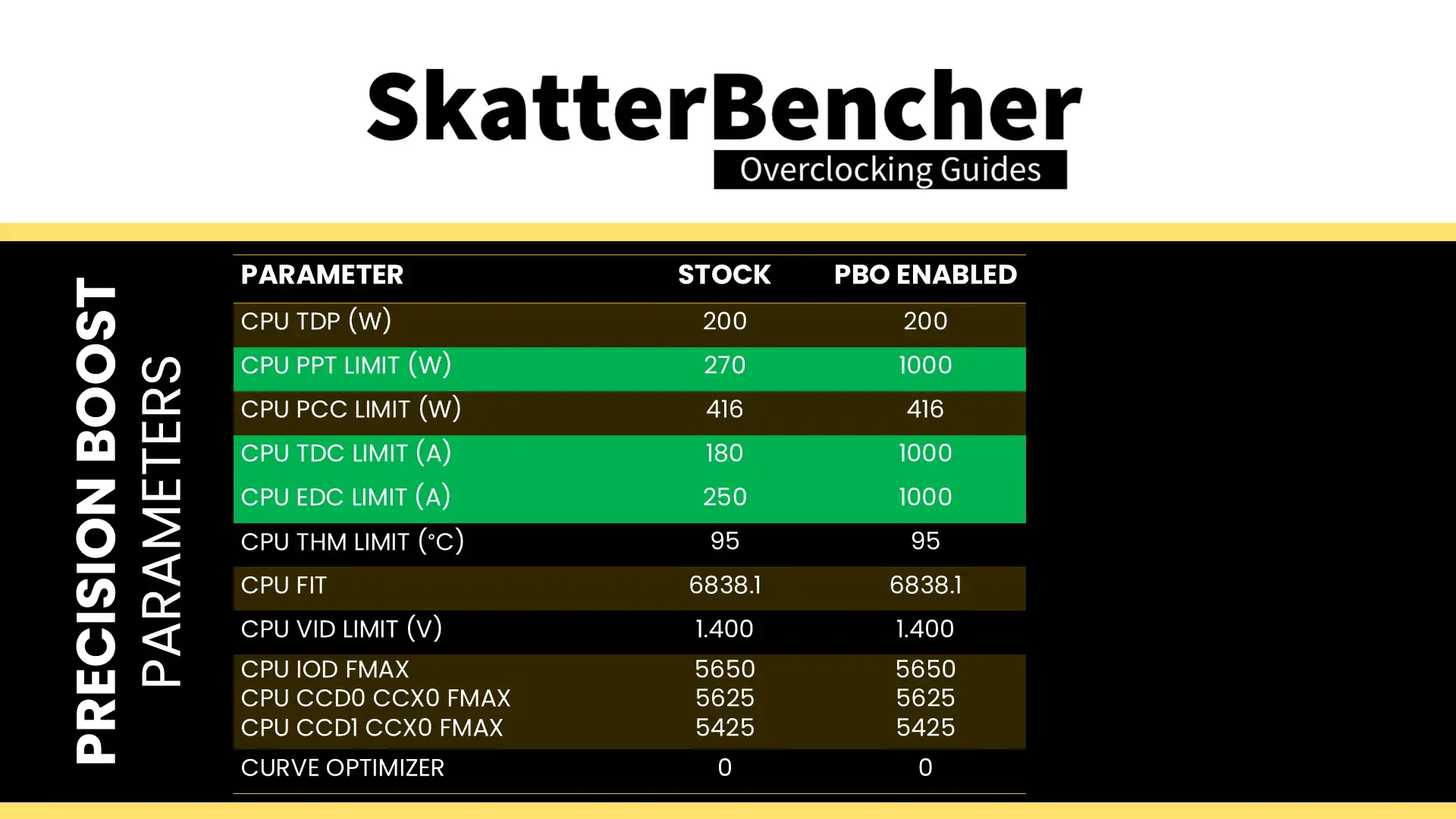
Before starting overclocking, we must check the system performance at default settings. The default Precision Boost 2 parameters for the Ryzen 9 9950X3D2 are as follows:
- PPT: 270 W
- TDP: 200 W
- PCC: 416 W
- TDC CPU: 180 A
- EDC CPU: 250 A
- THM: 95 C
- VID: 1.40 V
- CPU FMAX: 5650 MHz
- CCD0 FMAX: 5625 MHz
- CCD1 FMAX: 5425 MHz
- FIT: 6838.1
The Ryzen 9 9950X3D2 has two CCDs with eight Zen 5 CPU cores, each with their own factory-fused V/F Curve. We’ll talk about this more in depth later in the video.
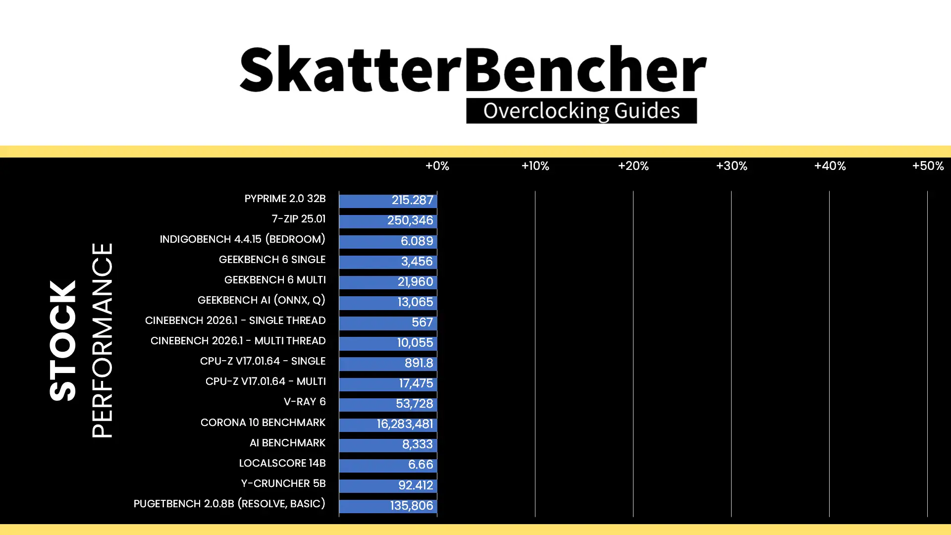
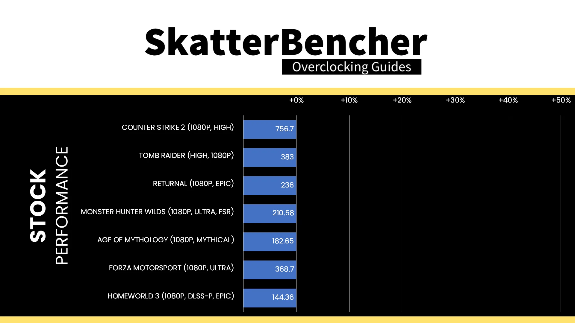
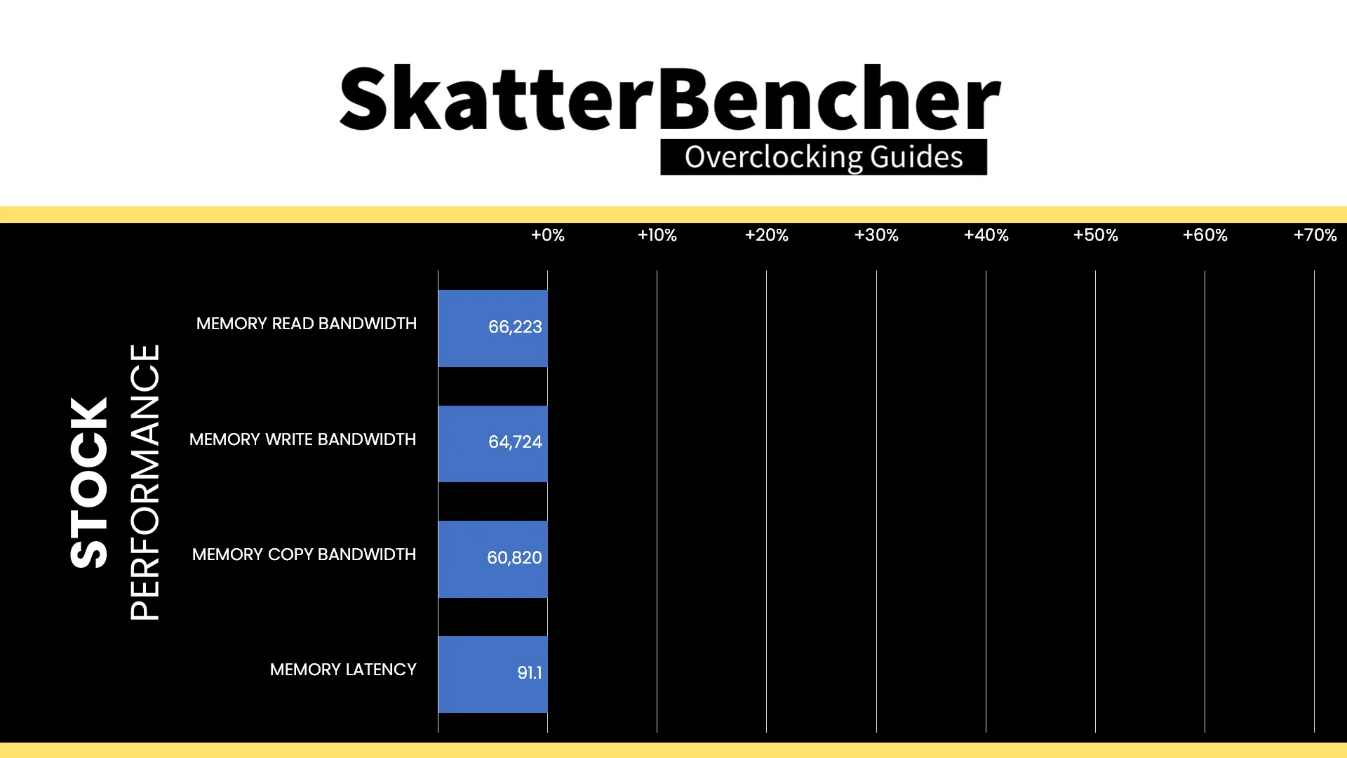
Here is the benchmark performance at stock:
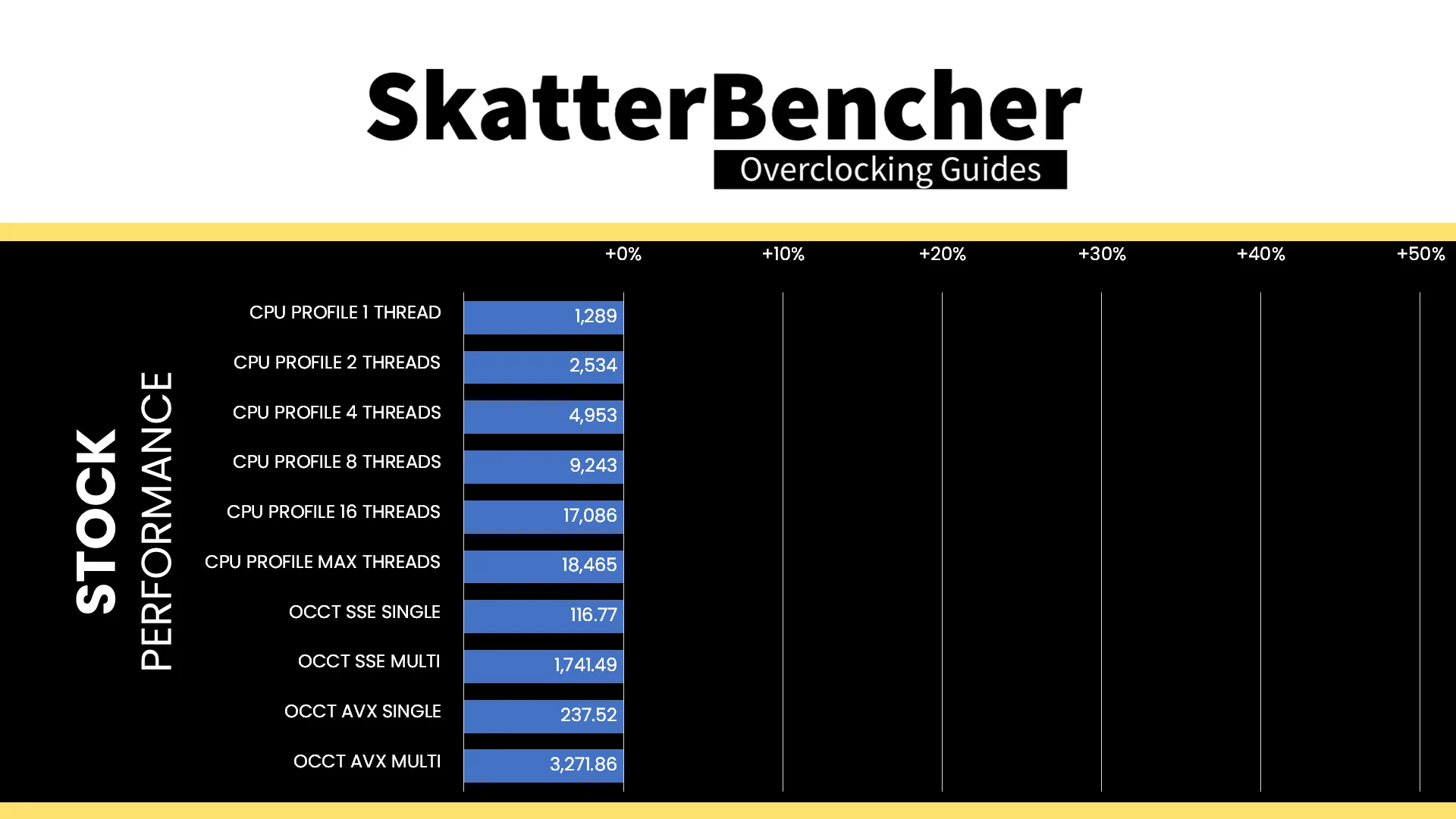
When running the OCCT CPU AVX-512 Stability Test, the average CPU CCD0 effective clock is 4565 MHz and CCD1 effective clock is 4542 MHz with 1.080 volts. The average CPU temperature is 80.2 degrees Celsius. The average CPU package power is 203.2 watts.
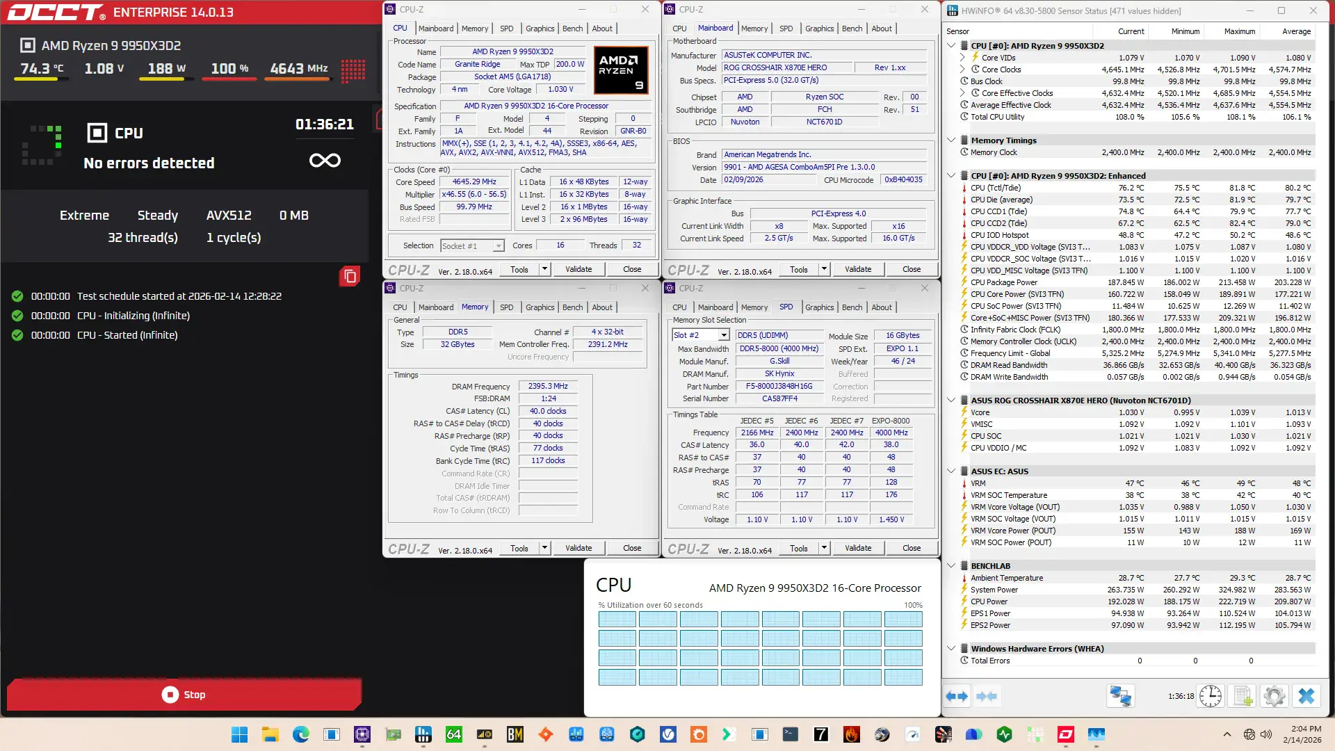
When running the OCCT CPU SSE Stability Test, the average CPU CCD0 effective clock is 4881 MHz and CCD1 effective clock is 4831 MHz with 1.156 volts. The average CPU temperature is 78.4 degrees Celsius. The average CPU package power is 230.8 watts.

Of course, we can increase the maximum power consumption limit using Precision Boost Overdrive. That’s what we’ll do in our first overclocking strategy.
However, before we get going, make sure to locate the CMOS Clear button. Pressing the Clear CMOS button will reset all your BIOS settings to default, which is helpful if you want to start your BIOS configuration from scratch. The Clear CMOS button is located on the back I/O of the motherboard.
OC Strategy #1: PBO + EXPO
In our first overclocking strategy, we simply take advantage of enabling AMD Precision Boost Overdrive 2 and AMD EXPO.
Precision Boost Overdrive 2
With the launch of Zen 5, AMD introduced a further improved version of the Precision Boost Overdrive overclocker’s toolkit, allowing for manual tuning of the parameters affecting the Precision Boost 2 frequency boost algorithm.
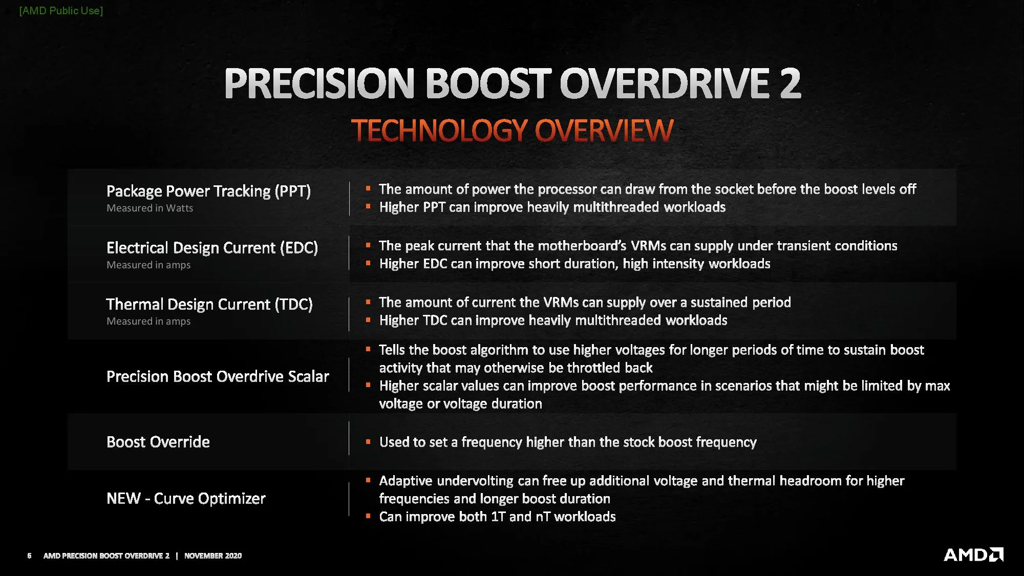
The Precision Boost Overdrive 2 toolkit for Zen 5 Ryzen processors includes the overclocking knobs from Zen+ (PPT, TDC, EDC), Zen 2 (Boost Override and Scalar), Zen 3 (Curve Optimizer), and the newly announced Curve Shaper for Zen 5.
There are essentially 3 levels of Precision Boost Overdrive
- AMD’s stock values, which can be set by disabling PBO
- The motherboard vendor values, which are programmed into BIOS to match the motherboard VRM specification and can be set by enabling PBO
- Custom values, which can be programmed by the end-user
In this overclocking strategy, we’re just enabling Precision Boost Overdrive, whereas, in the following strategies, we’ll explore tuning the parameters. By enabling Precision Boost Overdrive, we rely on the motherboard pre-programmed PBO parameters. We find that the following values have changed:
EXPO – Extended Profiles for Overclocking
EXPO stands for AMD Extended Profiles for Overclocking. It is an AMD technology that enables ubiquitous memory overclocking for AMD platforms supporting DDR5 memory.

EXPO allows memory vendors such as G.SKILL to program higher performance settings onto the memory sticks. If the motherboard supports EXPO, you can enable higher performance with a single BIOS setting. So, it saves you lots of manual configuration.
ASUS provides us with three EXPO options: EXPO I, EXPO II, and EXPO Tweaked. EXPO II loads the entire EXPO profile on the memory sticks, so that’s what I pick for this strategy. Check out SkatterBencher #95 to get a more detailed look at what EXPO I and EXPO Tweaked do in terms of settings and performance.
BIOS Settings & Benchmark Results
Upon entering the BIOS
- Go to the Extreme Tweaker menu
- Set Ai Overclock Tuner to EXPO II
- Enter the Precision Boost Overdrive submenu
- Set Precision Boost Overdrive to enabled
Then save and exit the BIOS.
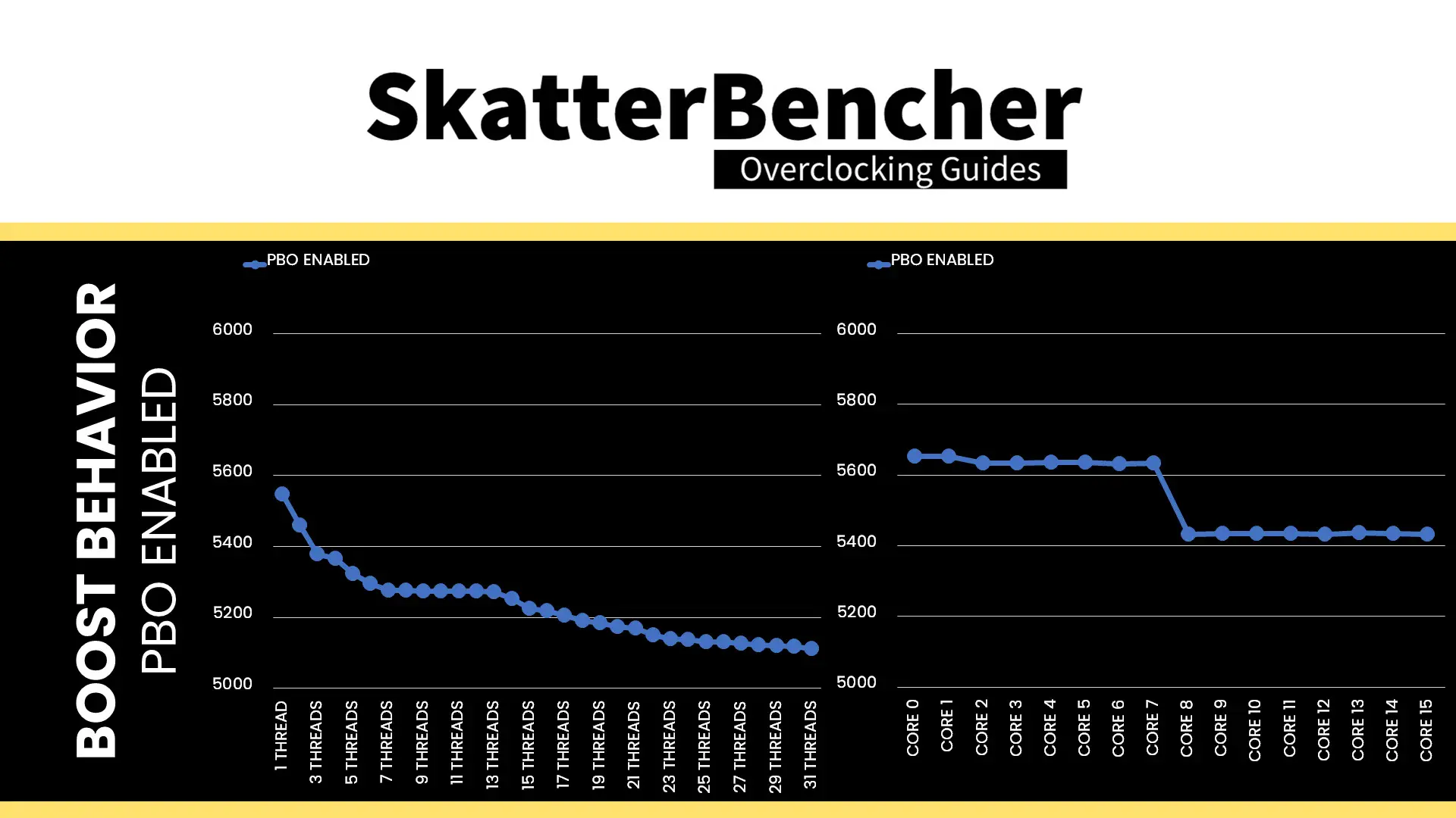
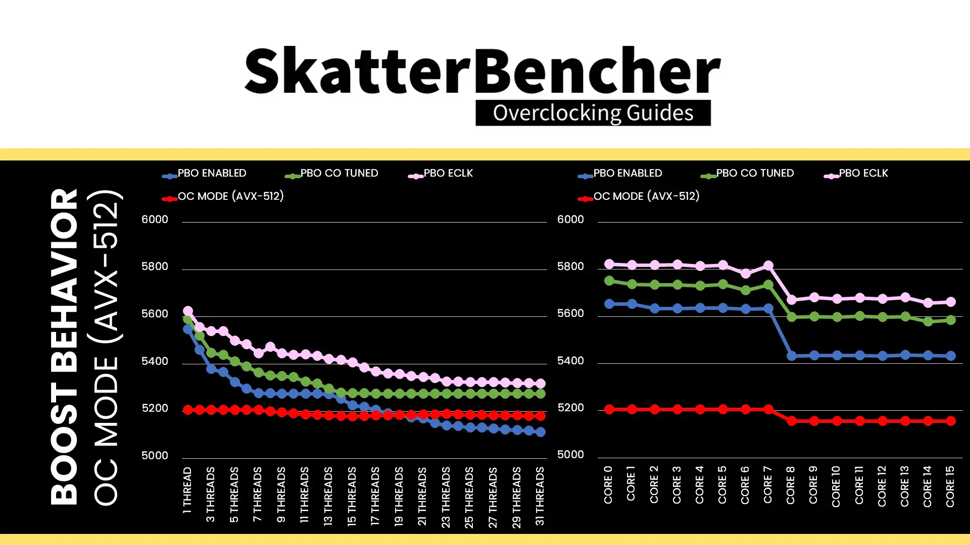
The boost frequency at 1 active thread is about 5547 MHz and the average boost frequency gradually trails off to 5112 MHz when all cores are active. In light single-threaded workloads, all cores in CCD0 can boost to over 5.6 GHz and all cores in CDD1 to over 5.4 GHz.
We re-ran the benchmarks and checked the performance increase compared to the default operation.
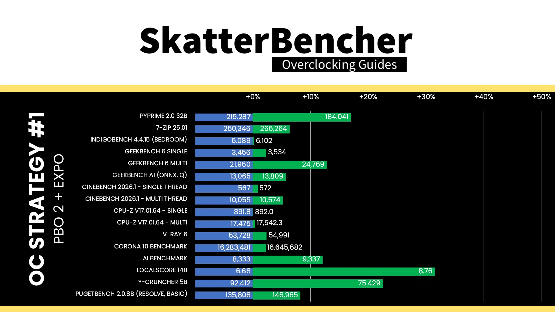
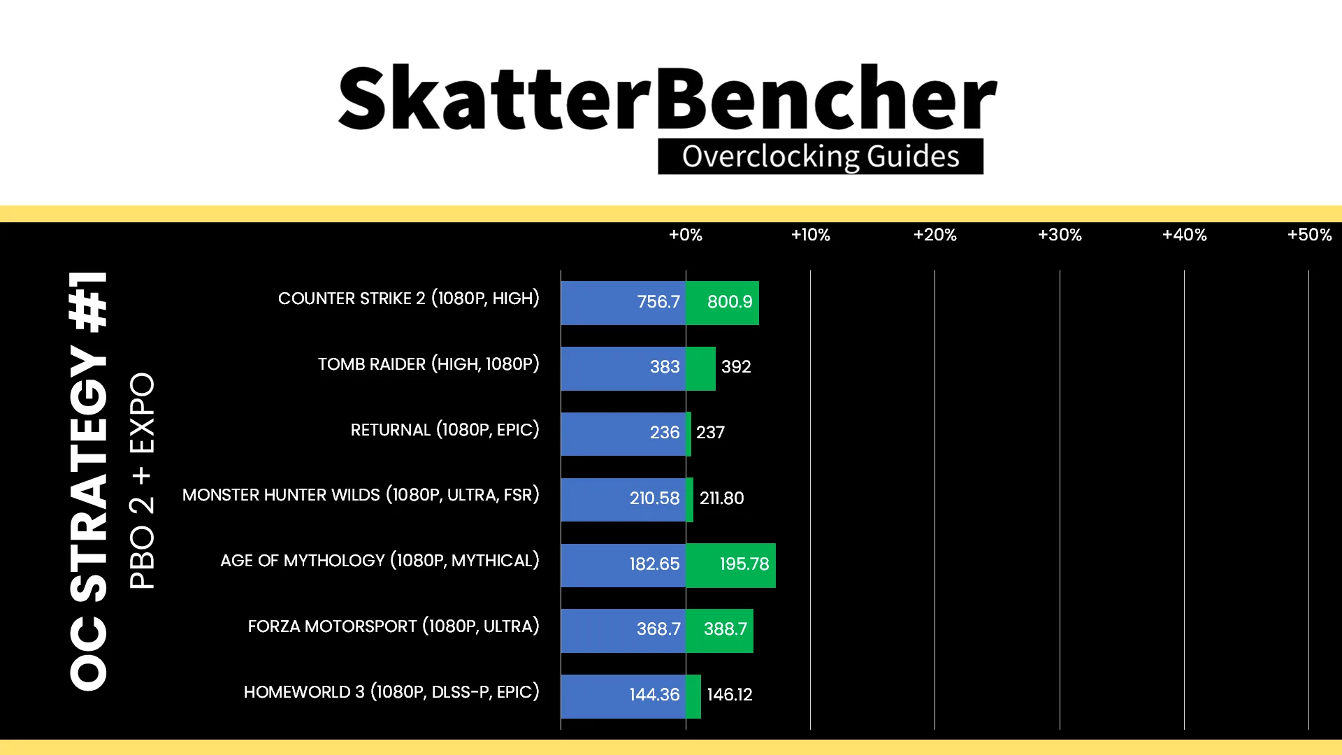
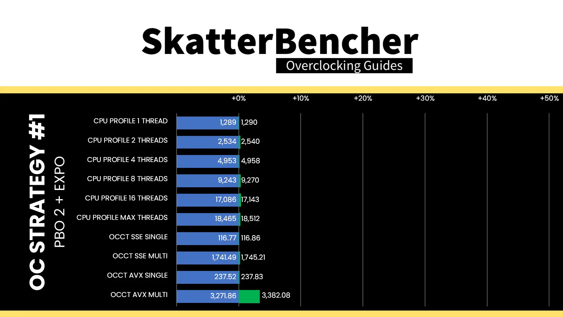

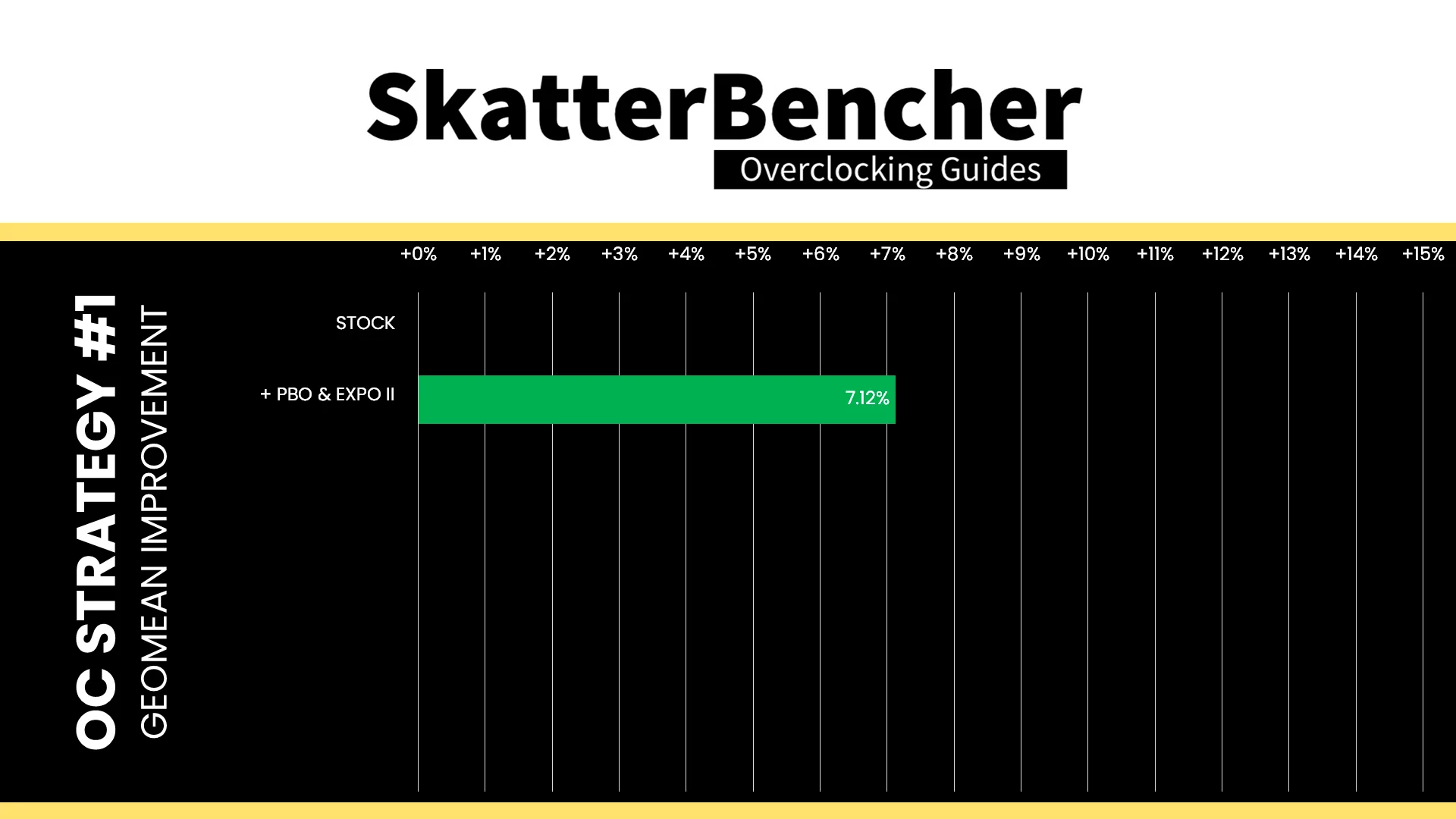
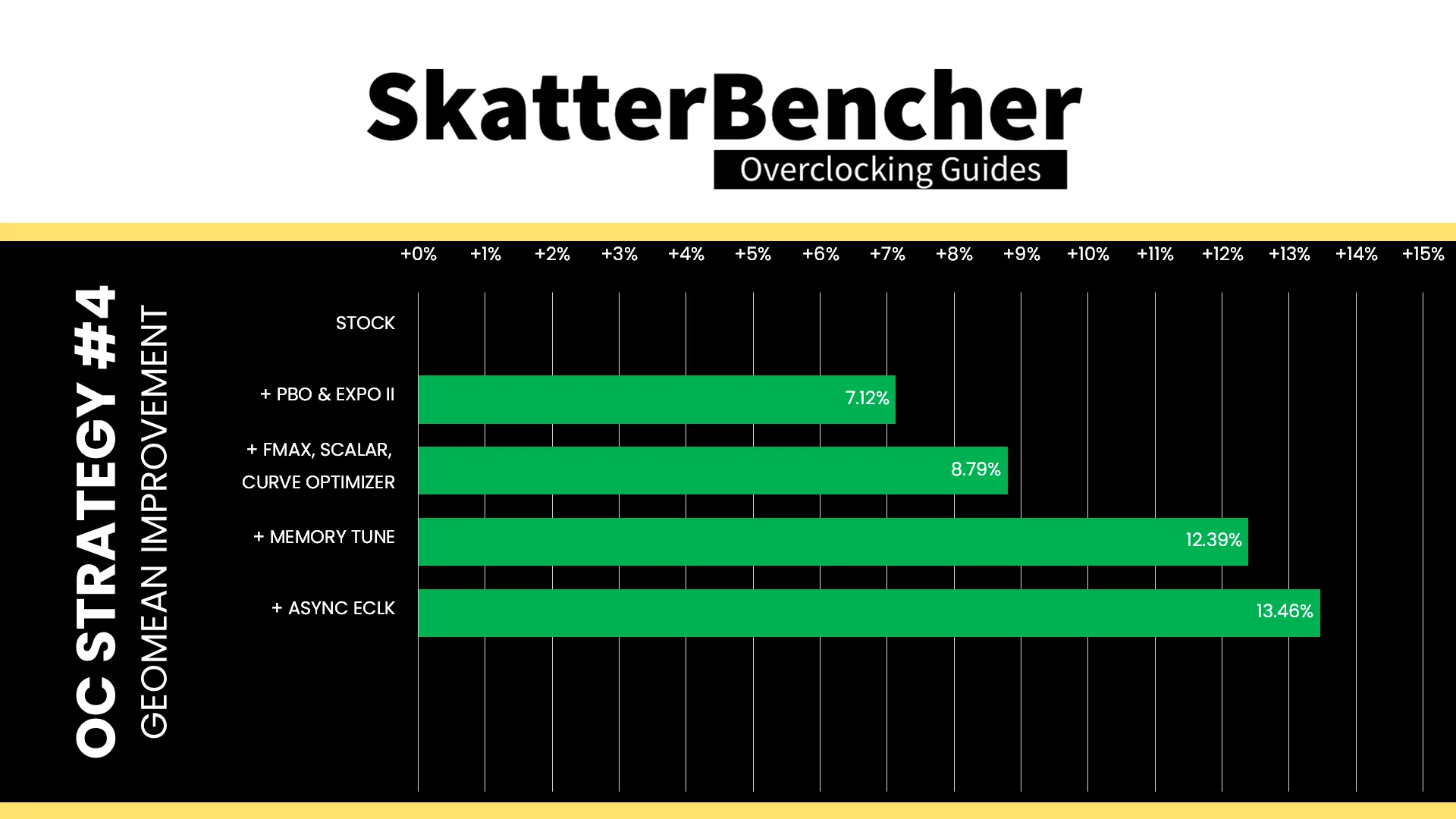
While the Ryzen 9 9950X3D2 has an 200W TDP, its actual power limit is 270W according to the Precision Boost 2 PPT parameter. Given we’re not seeing it hit this limit in the stock OCCT Stress Tests, unlocking the power limits is unlikely to give that much of a performance boost. However, the improved memory subsystem performance provides it a significant boost in memory-sensitive workloads. The Geomean performance speedup is +7.12%, and we get a maximum benchmark speedup of +31.53% in LocalScore.
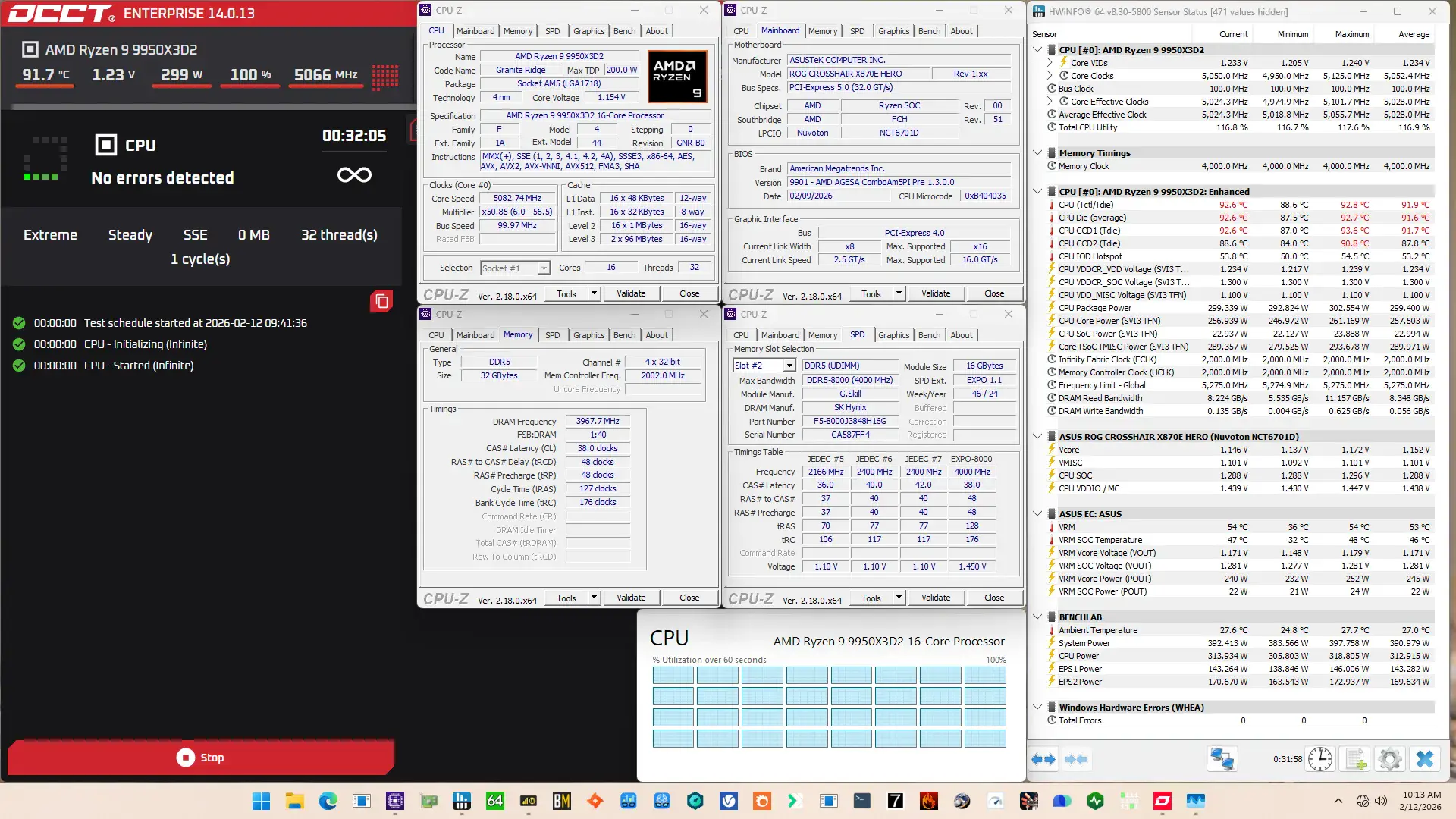
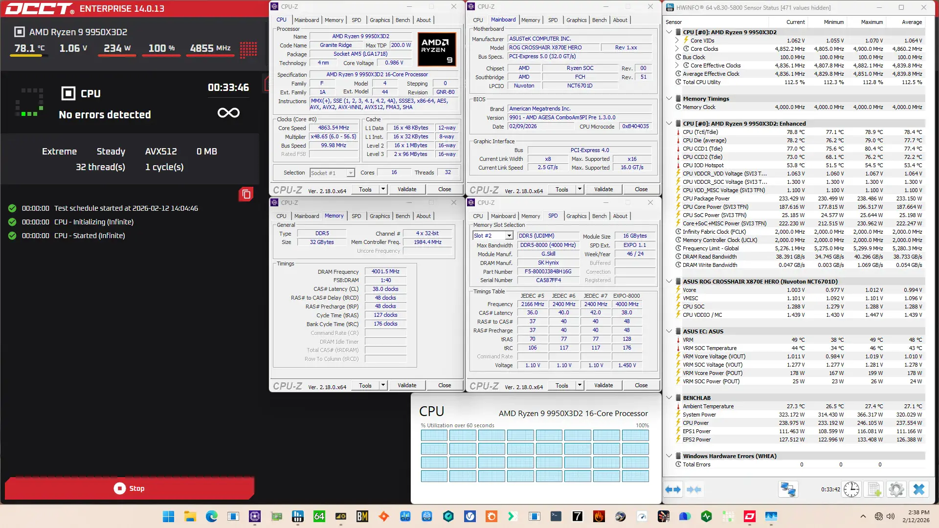
When running the OCCT CPU AVX-512 Stability Test, the average CPU CCD0 effective clock is 4525 MHz and CCD1 effective clock is 4498 MHz with 1.081 volts. The average CPU temperature is 81.7 degrees Celsius. The average CPU package power is 244.1 watts.

When running the OCCT CPU SSE Stability Test, the average CPU CCD0 effective clock is 5065 MHz and CCD1 effective clock is 4990 MHz with 1.234 volts. The average CPU temperature is 91.9 degrees Celsius. The average CPU package power is 299.4 watts.
OC Strategy #2: PBO Tuned
In our second overclocking strategy, we tune the CPU’s Precision Boost dynamic frequency technology using the Precision Boost Overdrive 2 toolkit.
PBO 2: Fmax Boost Override
Fused maximum frequency, or Fmax, is one of the Precision Boost infrastructure limiters constraining the CPU performance. Each chip in your CPU has a factory-fused Fmax, including the two CCDs and the IOD.
The IOD typically governs the overall CPU Fmax. For the Ryzen 9 9950X3D2, the IOD Fmax is 5650 MHz whereas CCD0 is limited to 5625 MHz and CCD1 is limited to 5425 MHz.
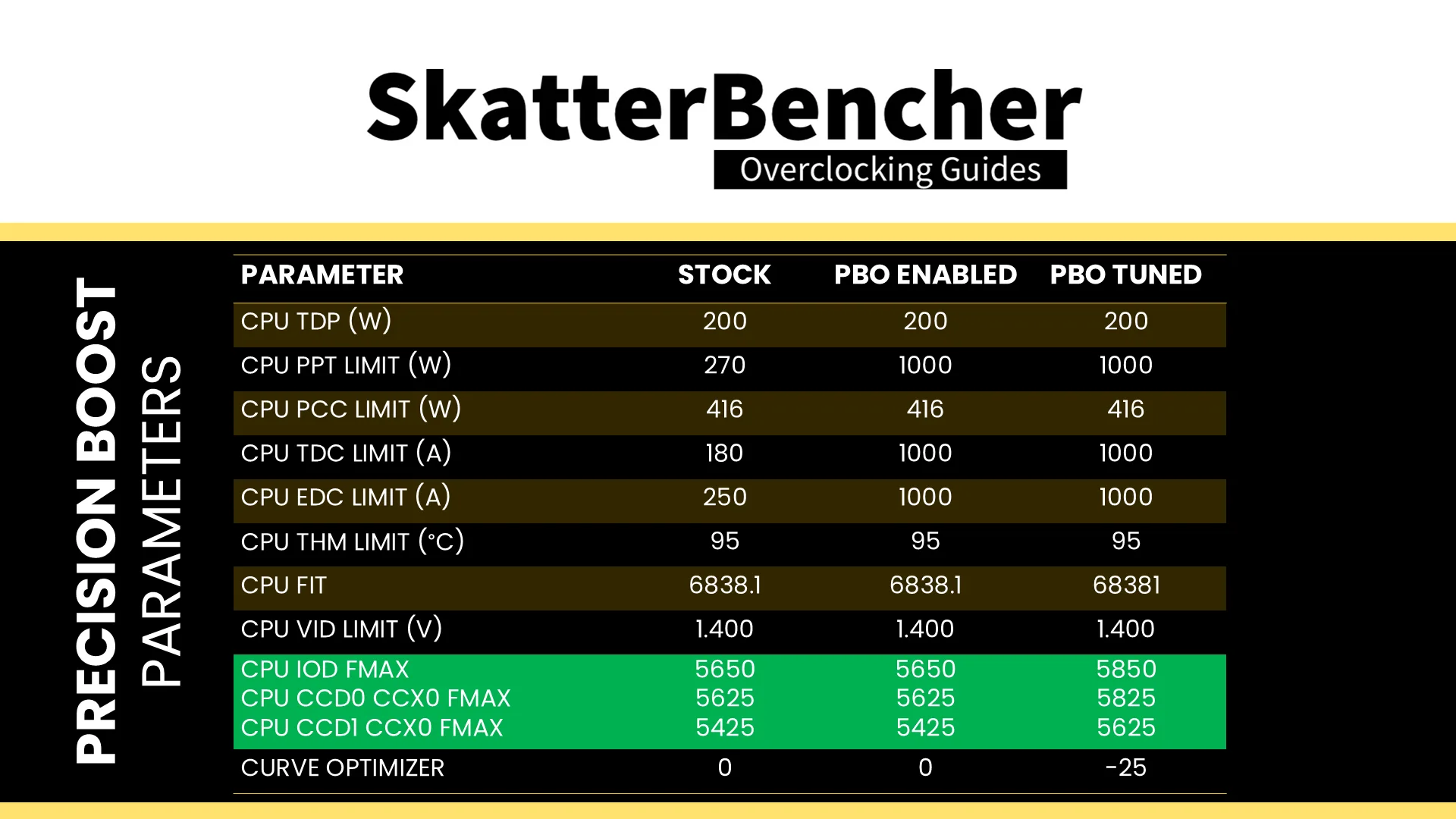
Boost Clock Override or Fmax Override is one of the tools available in the PBO 2 overclocker’s toolkit. It allows us to override the arbitrary clock frequency limit between -1000 MHz and +200 MHz. That’s been available in steps of 25 MHz since forever, but it seems that with Ryzen 9000 we can now set the Fmax in steps of as little as 1 MHz! The BIOS option still jumps in steps of 25 MHz, but with specialized tools we can set it to any frequency in the operating system.
The programmed CPU Fmax limit of the Ryzen 9 9950X3D2 is 5650 MHz. So, with a +200 Fmax Boost Override, the new maximum boost frequency is 5850 MHz. Note that the Fmax Boost Override applies to all chips on package, so the new CCD0 Fmax is 5825 MHz and the new CCD1 Fmax is 5625 MHz.
It’s important to note that the Fmax override only adjusts the upper ceiling of the frequency and doesn’t act as a frequency offset.
PBO 2: Scalar
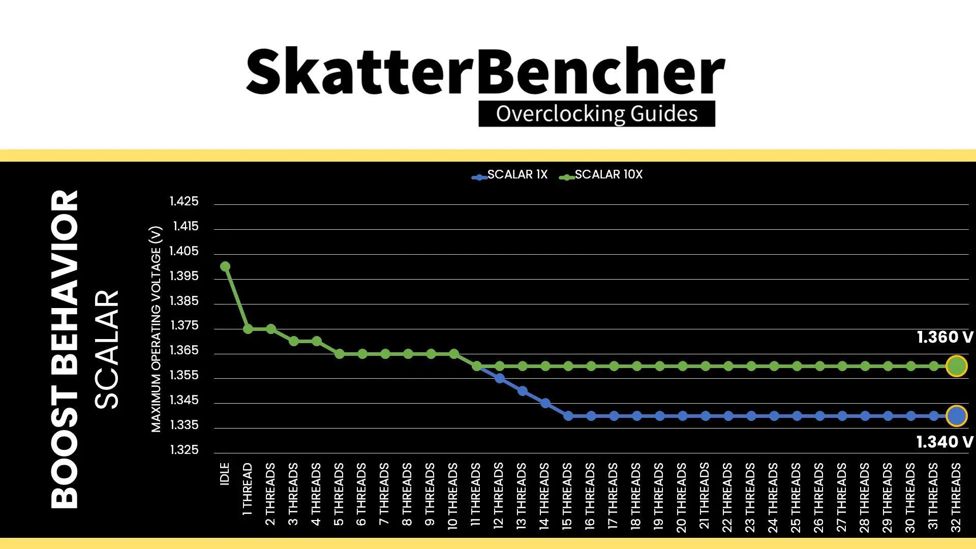
Scalar is a tool that allows the user to override the warranted silicon stress level, or FIT, to achieve higher frequency. You can adjust the maximum allowed FIT level to 10 times higher than the factory-fused limit. While the tool offers precise granularity, typically, you’ll find the available options to range between 1X and 10X in steps of 1 multiple.
The effect of increasing Scalar is that the Precision Boost algorithm more aggressively pursues higher voltages as it is less concerned with CPU lifespan. The tool’s relevance shifts from architecture to architecture as the FIT is only one of the Precision Boost infrastructure limiters managing the maximum allowed voltage.
For the Zen 5 Granite Ridge processors, it appears Scalar is making a comeback in the overclocking strategies because the chips are voltage limited. When all cores are active, the maximum voltage is 1.340V. The maximum voltage when a single thread is active is 1.375V.
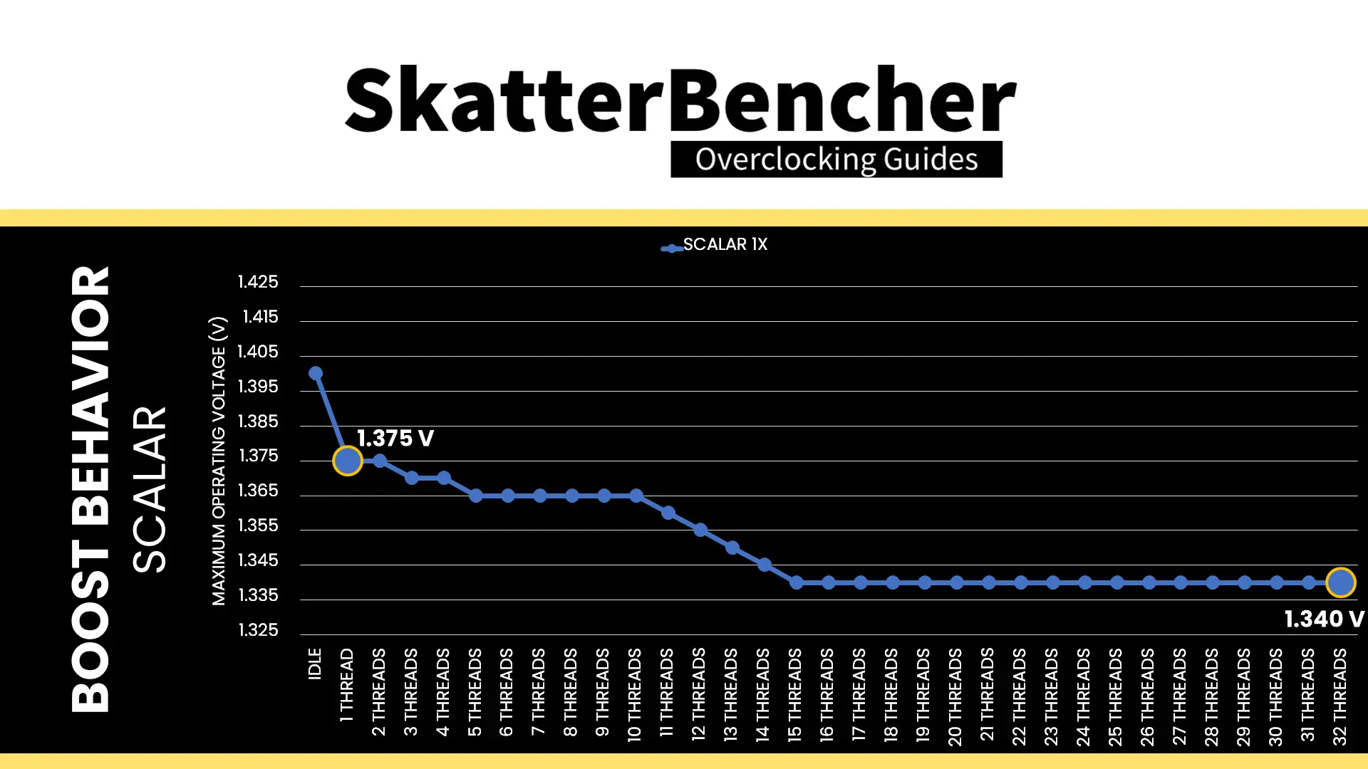
The programmed FIT value of this particular Ryzen 9 9950X3D2 is 6836.1. So, with a 10X scaler, the new FIT value is 68381. We find that in an all-core workload, the maximum voltage increased from 1.340V to 1.360V. That’s not a big increase, but in voltage-constraint scenarios, every little bit helps!
PBO 2: Curve Optimizer
Curve Optimizer has been one of the most important overclocking tools of the Precision Boost Overdrive 2 toolkit. It is most commonly known for its undervolting capabilities, but on AMD Ryzen CPUs, it kind of also works as an overclocking tool.
To explain how it works, let’s start with the basics: the voltage-frequency curve.
Simply put: a voltage-frequency curve describes the relationship between an operating frequency and the voltage required to operate at that frequency. Every modern SOC has a factory-fused voltage-frequency curve and uses this to dynamically adjust power consumption depending on the workload needs. This V/F curve is not readily available for us to read but we can use a couple of tools to approximate the curve. I explained how to do that in a different guide on this website.
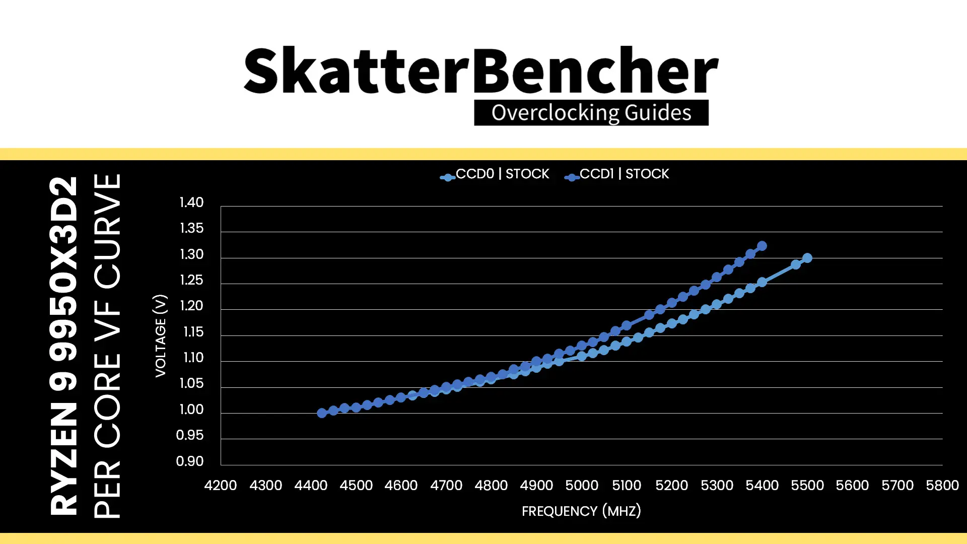
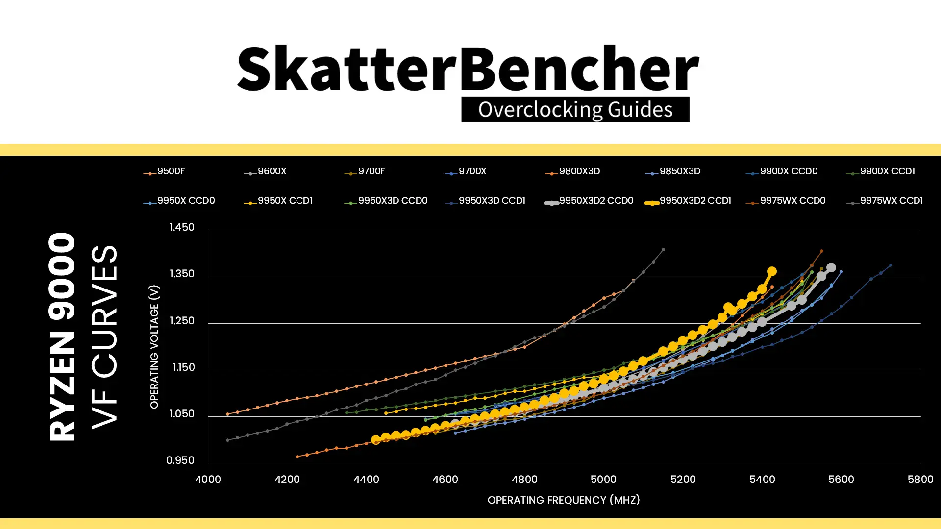
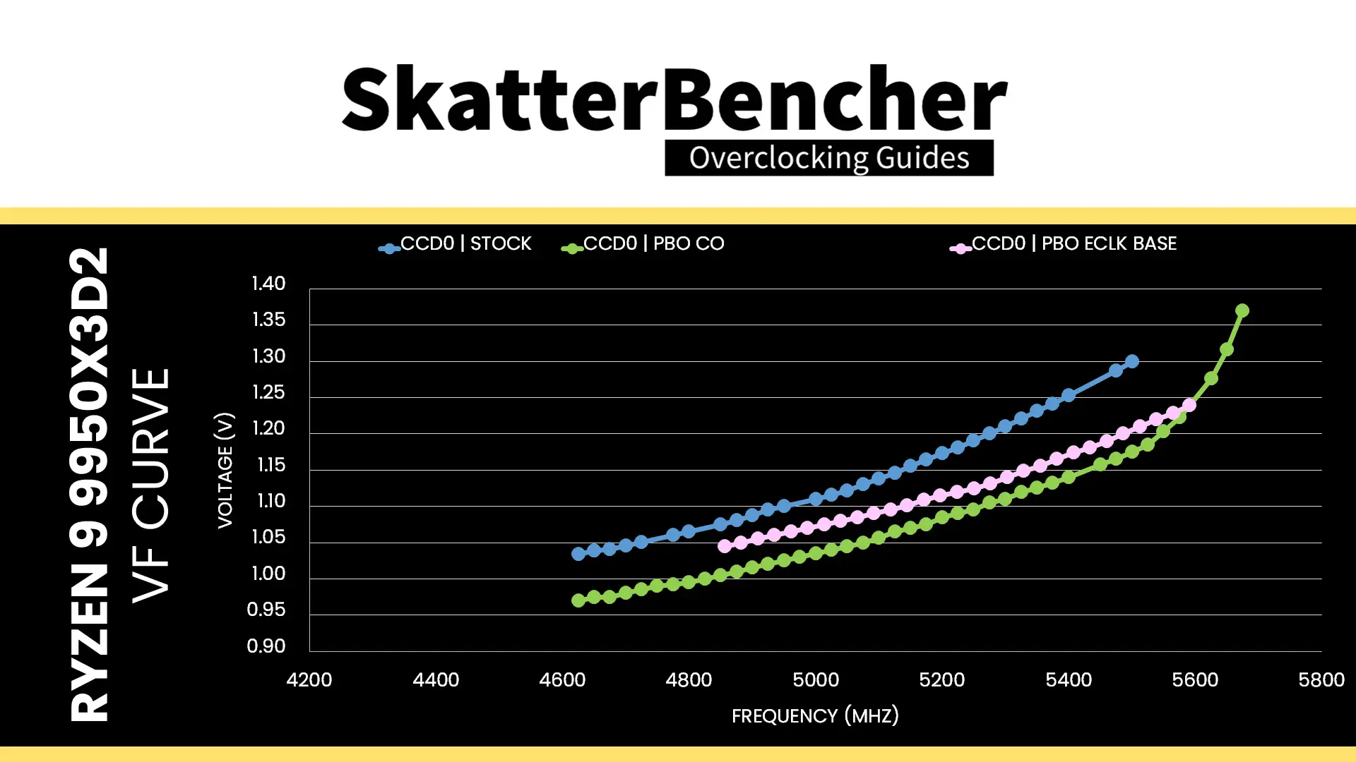
Here’s the default voltage-frequency curve of my Ryzen 9 9950X3D2 processor. You’ll find there’s in fact two distinct curves: one for each CCD. We can immediately make a simple and redundant observation: the higher the frequency, the higher the voltage. For example: CCD0 requires only 1.11V for 5000 MHz.

Although it’s not obvious from the V/F curve, the maximum allowed voltage is about 1.340V when all cores are active.
As I showed just a minute ago, we can use the Fmax Boost Override tool to increase the Fmax by another 200 MHz and extend the maximum allowed voltage using Scalar. That further extends the default V/F curve from 5625 to 5825 MHz for CCD0 and 5425 to 5625 MHz for CCD1. However, the Precision Boost limiter rules such as the Vlimit still apply and may restrict the maximum possible frequency.
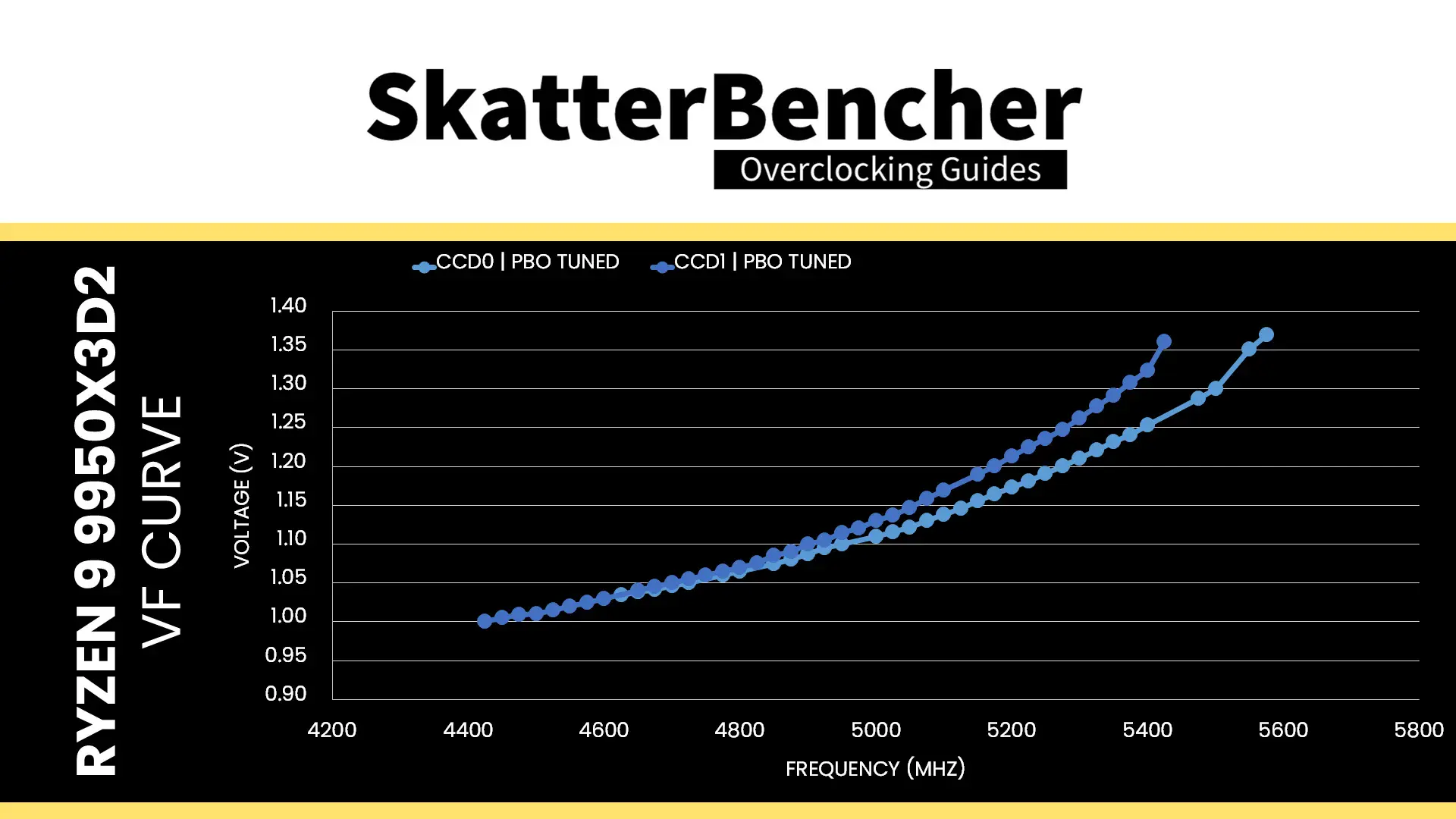
If we set a negative Curve Optimizer, we can shift the entire voltage-frequency curve along the voltage axis. And, suddenly, we need less voltage for every operating frequency. For example, at default, for 5.0 GHz CCD0 needed about 1.110V, However, with a -25 Curve Optimizer for CCD0, now we only need 1.035V! The same principle also applies to the other CCD.
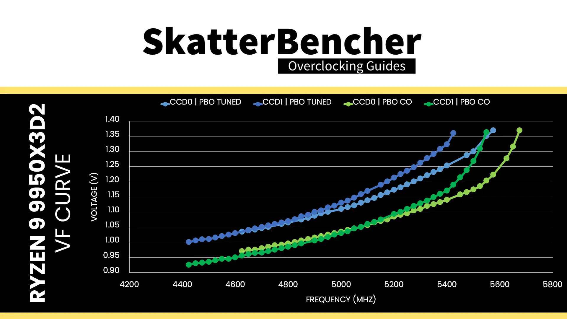
Moreover, the frequency is also boosting higher! The highest frequency with all cores in the CCD active has increased to 5675 MHz in CCD0 and 5550 MHz in CCD1. These higher frequencies are now possible because our Curve Optimizer undervolting pulled them below the increased voltage threshold.
Curve Optimizer is a powerful tuning tool. It’s simple but not simplistic. And the more you dig into the details of what it does, the more intricate it becomes to figure out how to apply it in a daily overclock. The traditional overclocking approach for AMD Ryzen CPUs is to undervolt by setting a negative curve optimizer. That helps in two ways.
- First, undervolting lowers the operating voltage, temperature, and power consumption.
- Second, as a consequence, the Precision Boost 2 algorithm can leverage the additional headroom to boost to higher frequencies.
So, you tend to get lower temperatures and extra performance. It’s a win-win. However, there are a couple of caveats to tuning with Curve Optimizer:
- Curve Optimizer impacts the entire voltage-frequency curve. So, it affects stability across the entire range of operating frequencies: from 600 to 6000 MHz.
- The same Curve Optimizer value impacts differently across the curve

If you’re lucky, your CPU’s undervolt margin matches how Curve Optimizer offsets the voltage across the curve. Then you’ll maximize the performance gains. But if you’re unlucky, and one part of your CPU’s V/F curve has a lot less margin, then your Curve Optimizer tuning journey will be a rough ride.
Curve Optimizer is available on a per CPU, per CCD, and per Core basis. For multi-CCD CPUs, I typically use the Per CCD curve optimizer approach because the CCD undervolting capabilities can vary wildly.
Ryzen 9 9950X3D2 Curve Optimizer Tuning Process
The manual tuning process for Curve Optimizer can become quite convoluted since it affects the CPU core voltage in all scenarios ranging from very light single-threaded workloads to heavy all-core workloads.
I want to emphasize this point and refer to my Ryzen 9 9950X overclocking guide, where I demonstrated that the V/F curve changes depending on the workload. With dynamic voltage-frequency scaling technologies like Precision Boost 2, it’s vital to test a wide variety of scenarios as opposed to just a heavy all-core workload pushing the power consumption to its limit. Sometimes your all-core AVX workload can be entirely stable, but you get bluescreens in games.
I identified five typical workloads that tend to show early signs of instability:
- OCCT AVX-512 Stress Test, which is a heavy AVX all-core workload
- Y-Cruncher Benchmark, which is a moderate AVX all-core workload
- 7-Zip Benchmark, which is a moderate AVX all-core workload
- OCCT Memory Stress Test, which is an extremely light all-core workload
- Y-Cruncher BKT, which is a light all-core workload
In this particular case, I found that Y-Cruncher was the earliest indicator of instability as I could pass OCCT AVX-512 with much more aggressive undervolt. Another way to think about this is that Y-Cruncher pushes the weakest part of this CPU’s VFT curve hence why it shows to be the most sensitive to undervolting.
When testing, I increase the negative Curve Optimizer setting in steps of 5 points, then check stability with each of these applications. Once I find an instability, I back off on the Curve Optimizer and check stability across the benchmark suite.
I ultimately ended up with a Curve Optimizer setting of -25 for both CCDs.
BIOS Settings & Benchmark Results
Upon entering the BIOS
- Go to the Extreme Tweaker menu
- Set Ai Overclock Tuner to EXPO II
- Switch to the Advanced menu
- Enter the AMD Overclocking submenu and click accept
- Enter the Precision Boost Overdrive submenu
- Set Precision Boost Overdrive to Advanced
- Set PBO Limits to Motherboard
- Set Precision Boost Overdrive Scalar Ctrl to Manual
- Set Precision Boost Overdrive Scalar to 10X
- Set CPU Boost Clock Override to Enabled (Positive)
- Set Max CPU Boost Clock Override to 200
- Enter the Curve Optimizer submenu
- Set Curve Optimizer to Per CCD
- Set CCD 0 and CCD 1 Curve Optimizer Sign to Negative
- Set CCD 0 and CCD 1 Curve Optimizer Sign to 25
- Set Curve Optimizer to Per CCD
- Leave the Curve Optimizer submenu
- Enter the Precision Boost Overdrive submenu
Then save and exit the BIOS.
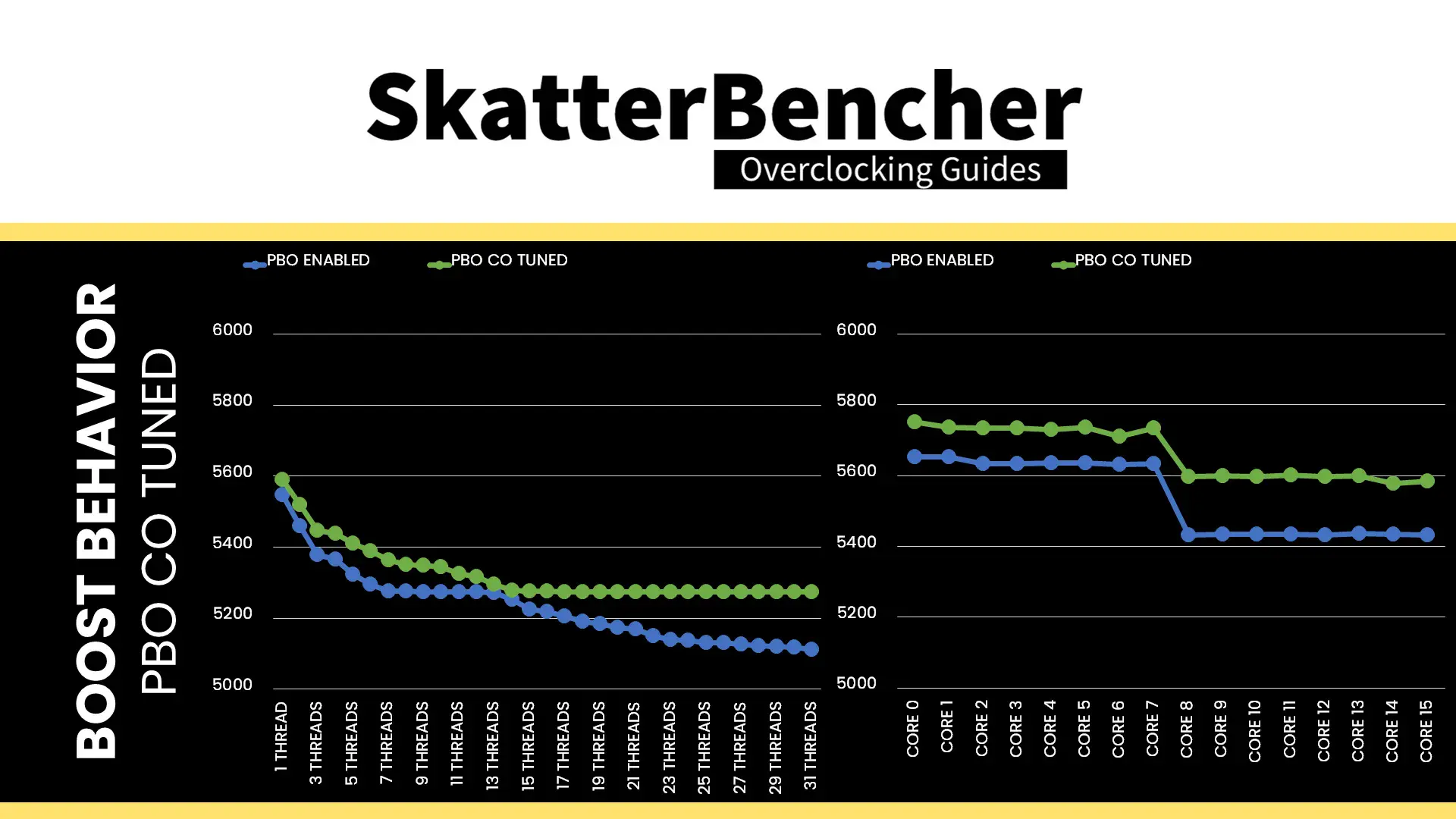
The boost frequency at 1 active thread is about 5589 MHZ and the average boost frequency gradually trails off to 5274 MHz when all cores are active. In light single-threaded workloads, all cores in CCD0 can boost to over 5.7 GHz and three cores in CDD1 to over 5.6 GHz.
We re-ran the benchmarks and checked the performance increase compared to the default operation.
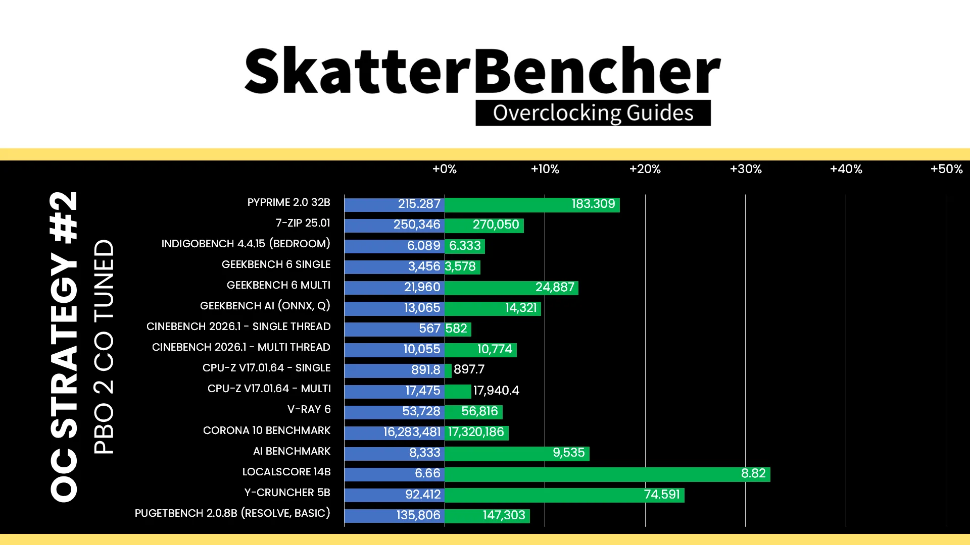
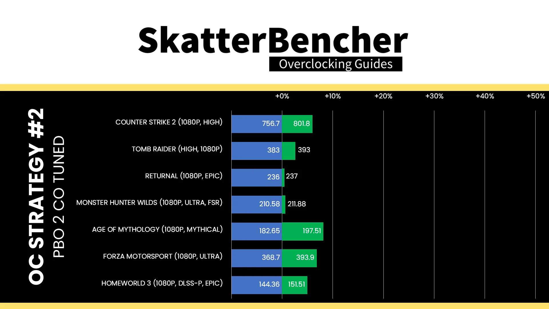


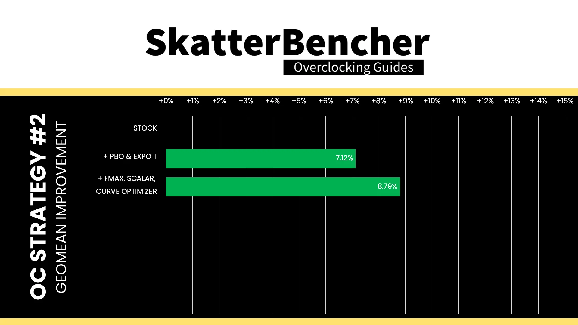
Undervolting with Curve Optimizer is a Ryzen overclocker’s best friend and has been for a long time. It provides this Ryzen 9 9950X3D2 with a nice frequency and performance bump. The geomean performance speedup improves by one and a half percentage points, and we get a maximum benchmark speedup of +32.43% in LocalScore.
When running the OCCT CPU AVX-512 Stability Test, the average CPU CCD0 effective clock is 4867 MHz and CCD1 effective clock is 4852 MHz with 1.064 volts. The average CPU temperature is 78.4 degrees Celsius. The average CPU package power is 233.2 watts.
When running the OCCT CPU SSE Stability Test, the average CPU CCD0 effective clock is 5274 MHz and CCD1 effective clock is 5215 MHz with 1.216 volts. The average CPU temperature is 92.2 degrees Celsius. The average CPU package power is 302.7 watts.

Intermezzo: Ryzen 9 9950X3D2 V/F Curve
Before I continue the tuning process, I want to spend a couple more minutes talking about the Ryzen 9 9950X3D2 V/F curve.
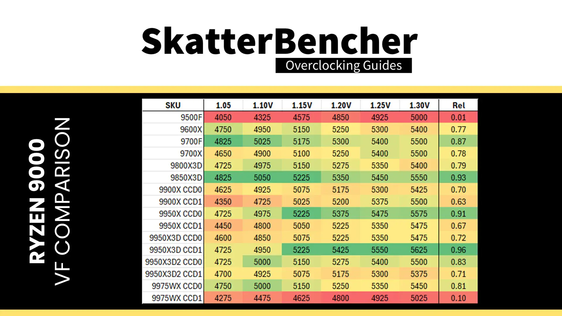
Compared to the other Ryzen gaming chips, the 9950X3D2 CCDs are in the middle of the pack. Not the best but certainly not the worst. And the same applies if we just look at the X3D CCDs, though CCD1 has the lowest rating from my testing.
I’ve made the argument a couple times before but I’ll re-iterate again: the flexibility of AMD’s CPU packaging makes it relatively easy to repurpose lower-grade CCDs into higher-priced SKUs. Specifically, by lower-grade I refer to the CCDs with limited Fmax capability which would typically find its way to Ryzen 7 or Ryzen 5 product segments. But, by adding on 3D V-cache technology, the CCD’s performance in cache-not-frequency-sensitive workloads (like certain games) puts it firmly in the upper Ryzen 7 and Ryzen 9 categories.
OC Strategy #3: Memory Tuned
In our third overclocking strategy, we delve into tuning the memory subsystem performance.
On AMD Granite Ridge processors, the memory subsystem consists of three major parts: the infinity fabric, the unified memory controller, and the system memory. They’re more commonly referred to as FCLK, UCLK, and MCLK.
First-generation Ryzen overclockers know that these parts used to be tightly coupled together, but on modern Ryzen processors like the Ryzen 9 9950X3D2, we can tune them independently.
Infinity Fabric Tuning
The Fabric frequency, or FCLK, is generated by the SOC PLL, derived from a 100 MHz reference clock input. The reference clock is multiplied by the FCLK ratio, which you can configure in the BIOS.
The standard operating frequency of the infinity fabric is 1800 MHz, but on many boards, you’ll find it runs at 2 GHz when EXPO is enabled. That said, it doesn’t seem there’s much overclocking headroom beyond 2 GHz. I managed to set 2200 MHz for this overclocking strategy, however anything higher couldn’t boot reliably. Not even with voltage adjustments.
Speaking of voltage: the infinity fabric voltage is provided by the VDDG voltage supply, derived via an integrated voltage regulator from the VDDCR_MISC voltage rail. There is a total of four VDDG voltage rails available for manual adjustment:
- CCD0-CCD VDDG: signals sent from CCD0 to IOD are sent at this voltage.
- CCD0-IOD VDDG: signals sent from IOD to CCD0 are sent at this voltage.
- CCD1-CCD VDDG: signals sent from CCD1 to IOD are sent at this voltage.
- CCD1-IOD VDDG: signals sent from IOD to CCD0 are sent at this voltage.
Note that the VDDG voltage does not adjust automatically with VDDCR_MISC. So, if you need to increase VDDG, for example, to support higher memory frequency, you need to change it manually.
Memory Controller Tuning
AMD Granite Ridge has two DDR5 Unified Memory Controllers, or UMC in short, and each provides two 32-bit memory channels. The memory controllers are located in the IO die and are identical to the memory controllers on Ryzen 7000 “Raphael” processors.
The Unified Memory Controller frequency, or UCLK, is derived from the UMCCLK, one of the SOC PLLs. The UMCCLK is driven by a 100 MHz reference clock derived from either an internal or external clock generator.
The memory controller frequency is tied directly to the system memory frequency. It can run either at the same or half its frequency. At default, the memory controller runs at the same frequency as the system memory at 2400 MHz. However, we find that when enabling EXPO, the motherboard auto-rules will drop the memory controller frequency to half the memory frequency.
We could easily force the memory controller to run at the same frequency as the system memory by setting UCLK DIV1 Mode to UCLK=MEMCLK. However, that’s only possible if we run the memory at around DDR5-6000. Since our memory is running at DDR5-8000, we’re forced to maintain a UCLK frequency that’s half that of the memory frequency.
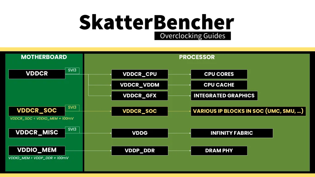
The VDDCR_SOC voltage rail provides the external power for multiple internal voltage regulators on SOC for the various IP blocks, including the memory controller. The VDDIO_MEM voltage rail is related as it provides the external power for the VDDP DDR5 bus signaling.
A nice benefit of running DDR5-8000 with the memory controller at half the memory frequency is that we can run the SOC voltage lower as well. The BIOS auto-rules will usually increase the SOC voltage to 1.25V or higher to increase the overclocking headroom, but with DDR5-8000 we don’t need that much voltage. In my case, I could lower it to 1.15V and still have a stable system.
It is essential to know that the VDDCR_SOC voltage must always be lower than VDDIO_MEM_S3 + 100mV. The default VDDCR_SOC voltage is 1.05V and can be set to 1.30V under ambient conditions. That’s typically required for running the memory controller in sync with the memory at DDR5-6400. However, we need LN2 mode enabled for higher voltages.
System Memory Timings Tuning
The last piece of the memory subsystem performance tuning is tuning the memory timings. For this, I rely in part on ASUS’ Memory Presets technology.
ASUS Memory Presets
ASUS Memory Presets is an ASUS overclocking technology that provides a selection of memory-tuning presets for specific memory ICs. The presets will adjust the memory timings and voltages.
The ROG Crosshair X870E Hero motherboard sports fourteen memory profiles for a variety of memory ICs and configurations. Since we’re interested in simply adjusting the memory timings, we can try the Hynix 7600MHz 1.45V 2x16GB SR preset.
Memory Timings Tuning
The Hynix 7600 memory preset turned out not to be stable at EXPO-8000 because it just wouldn’t boot. But no cause for alarm because we’ve seen this in previous overclocking guides as well.
The first step in looking for stability is always just to reduce the memory frequency by a couple of steps. While that reduces performance, obviously, it’s much faster to fine-tune than digging into individual sub timings. In my case, I found the kit to be stable at DDR5-7800 but only after changing the TREFI timing to 32767.
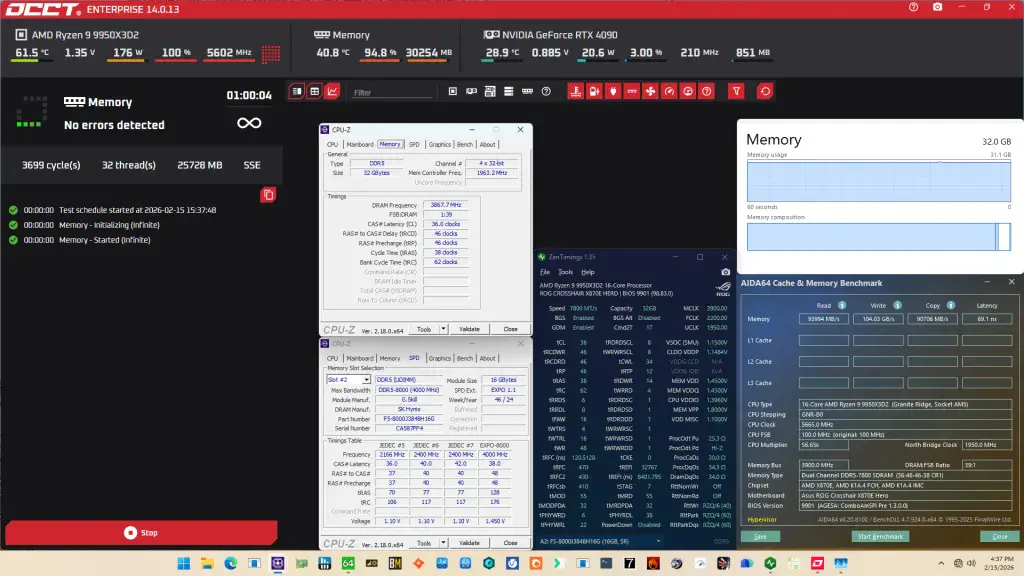
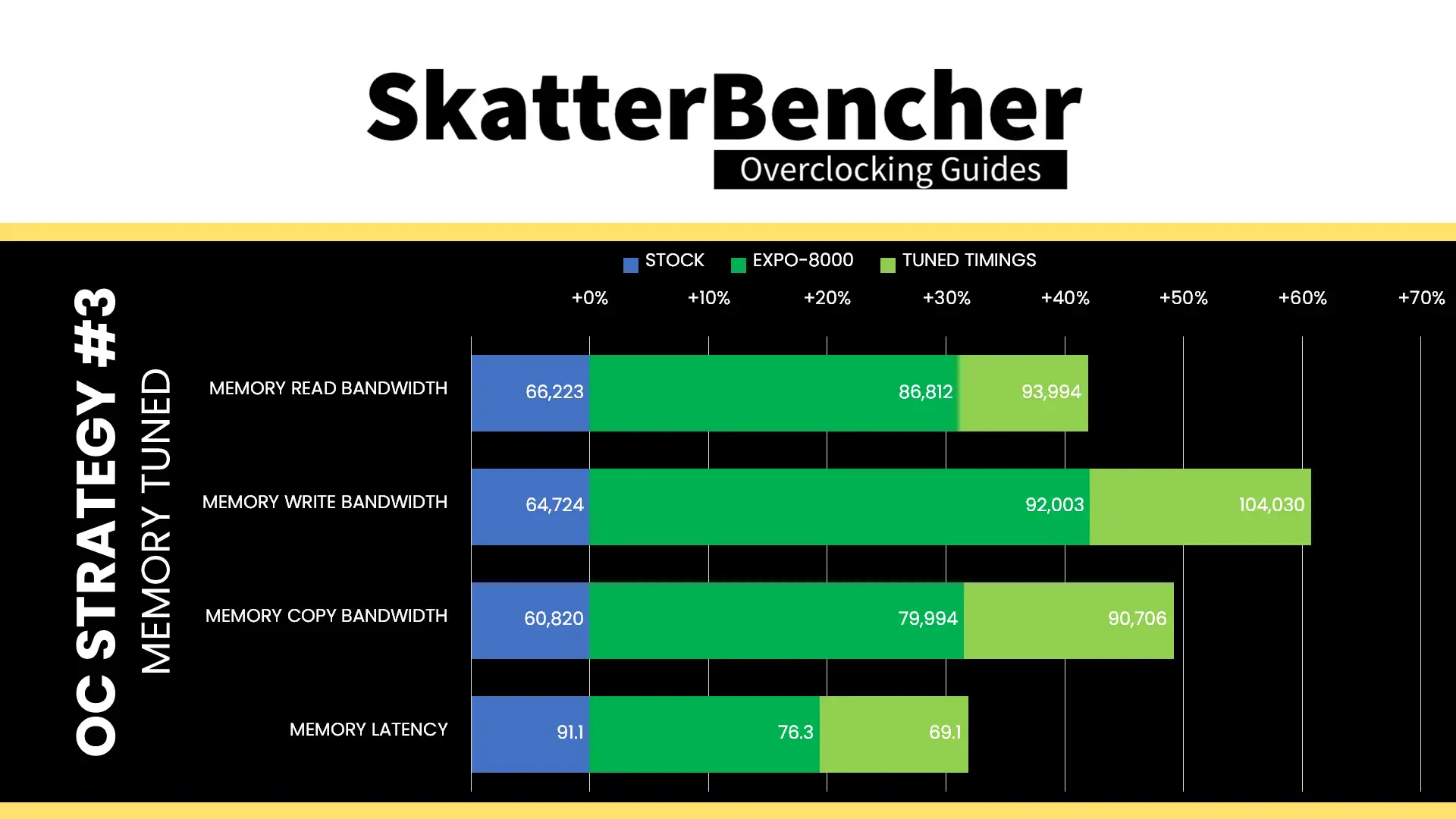
After the tuning, our AIDA64 performance improved quite significantly. We got about +30% extra bandwidth and 20% lower latency by enabling EXPO. The memory tuning then added another 12-to-20% improvement on top of that.
BIOS Settings & Benchmark Results
Upon entering the BIOS
- Go to the Extreme Tweaker menu
- Set Ai Overclock Tuner to EXPO II
- Set Memory Frequency to DDR5-7800
- Enter the DRAM Timing Control submenu
- Enter the Memory Presets submenu
- Select Load Hynix 7600MHz 1.45V 2x16GB SR and click OK
- Leave the Memory Presets submenu
- Set TREFI to 32767
- Enter the Memory Presets submenu
- Leave the DRAM Timing Control submenu
- Set VDDSOC Voltage Override to Offset
- Set VDDSOC Voltage Offset to 0
- Switch to the Advanced menu
- Enter the AMD Overclocking submenu and click accept
- Enter the DDR and Infinity Fabric Frequency/Timings submenu
- Enter the Infinity Fabric Frequency and Dividers submenu
- Set Infinity Fabric Frequency and Dividers to 2200 MHz
- Leave the Infinity Fabric Frequency and Dividers submenu
- Enter the Infinity Fabric Frequency and Dividers submenu
- Leave the DDR and Infinity Fabric Frequency/Timings submenu
- Enter the Precision Boost Overdrive submenu
- Set Precision Boost Overdrive to Advanced
- Set PBO Limits to Motherboard
- Set Precision Boost Overdrive Scalar Ctrl to Manual
- Set Precision Boost Overdrive Scalar to 10X
- Set CPU Boost Clock Override to Enabled (Positive)
- Set Max CPU Boost Clock Override to 200
- Enter the Curve Optimizer submenu
- Set Curve Optimizer to Per CCD
- Set CCD 0 and CCD 1 Curve Optimizer Sign to Negative
- Set CCD 0 and CCD 1 Curve Optimizer Sign to 25
- Set Curve Optimizer to Per CCD
- Leave the Curve Optimizer submenu
- Leave the Precision Boost Overdrive submenu
- Enter the SoC Voltage submenu
- Set SoC Voltage to 1150
- Enter the DDR and Infinity Fabric Frequency/Timings submenu
Then save and exit the BIOS.
We re-ran the benchmarks and checked the performance increase compared to the default operation.
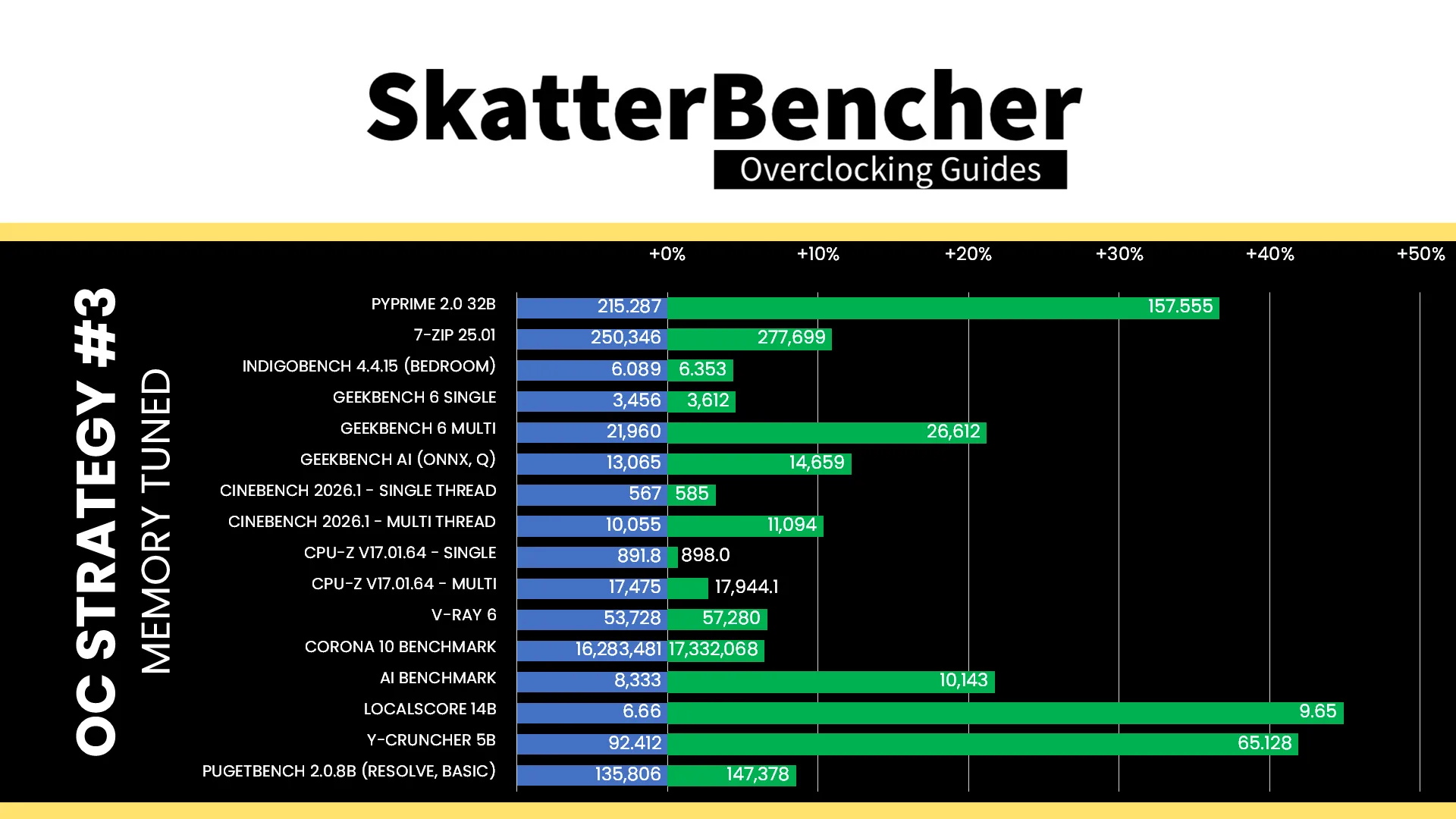
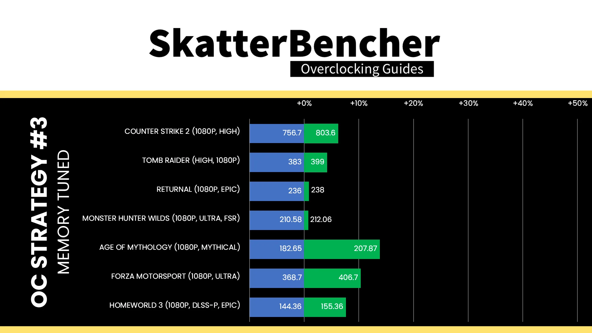
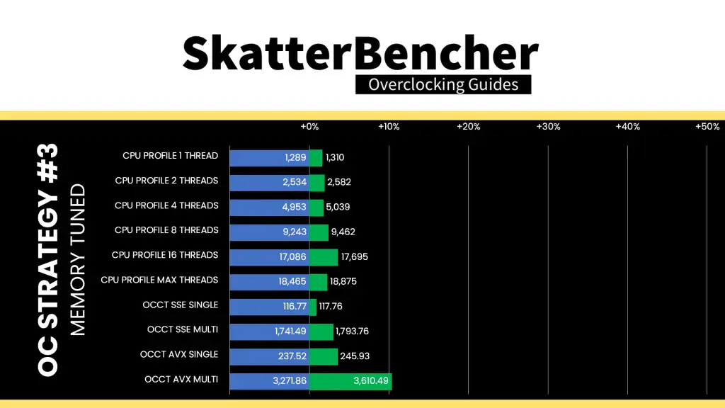
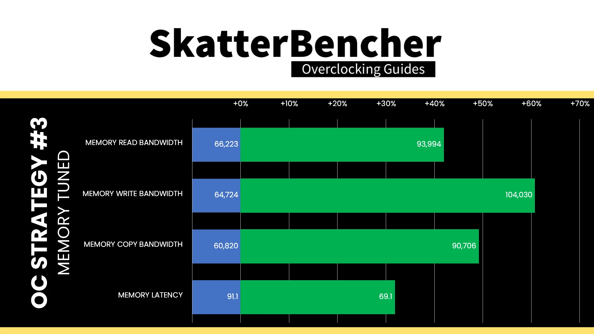
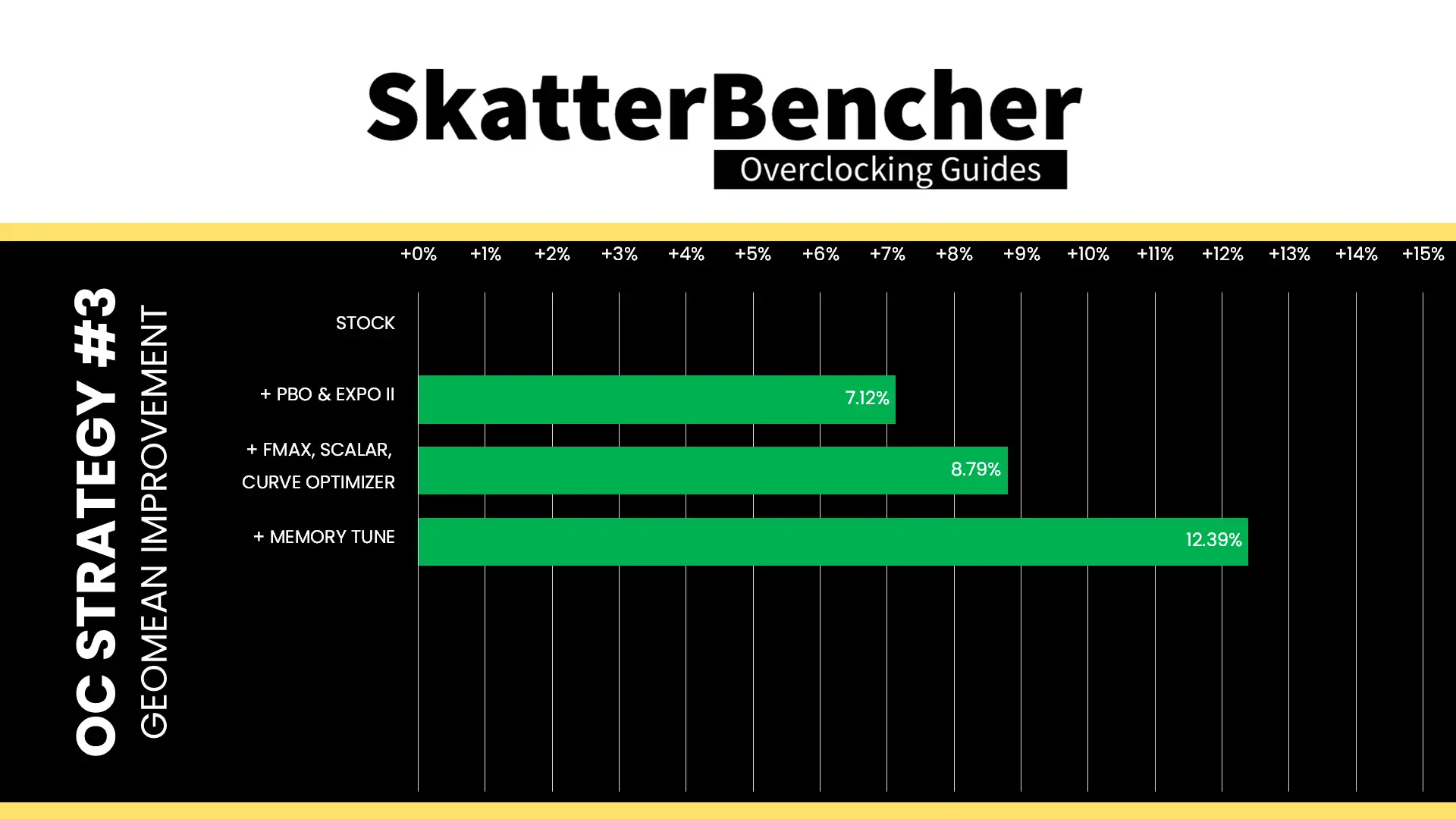
As we’ve seen with other modern platforms, tuning the memory timings can have a not insignificant impact on system performance, especially in workloads which are memory dependent. I was expecting memory performance to have less impact with this dual X3D CPU, but it seems that despite the extra L3 cache it still benefits tremendously from higher speed memory. Especially in workloads like Y-Cruncher and LocalScore. The Geomean performance speedup improves another four and a half percentage points and we get a maximum benchmark performance improvement of +44.89% in LocalScore.
When running the OCCT CPU AVX-512 Stability Test, the average CPU CCD0 effective clock is 4816 MHz and CCD1 effective clock is 4833 MHz with 1.062 volts. The average CPU temperature is 78.8 degrees Celsius. The average CPU package power is 236.6 watts.

When running the OCCT CPU SSE Stability Test, the average CPU CCD0 effective clock is 5274 MHz and CCD1 effective clock is 5180 MHz with 1.215 volts. The average CPU temperature is 93.1 degrees Celsius. The average CPU package power is 290.0 watts.
OC Strategy #4: Async ECLK & Curve Shaper
In our fourth overclocking strategy, we take advantage of ECLK mode. ECLK stands for external clock and is precisely what the term suggests: an external clock generator. With the external clock generator, we can warp the Precision Boost V/F curve to achieve higher frequencies.
Granite Ridge ECLK Overview
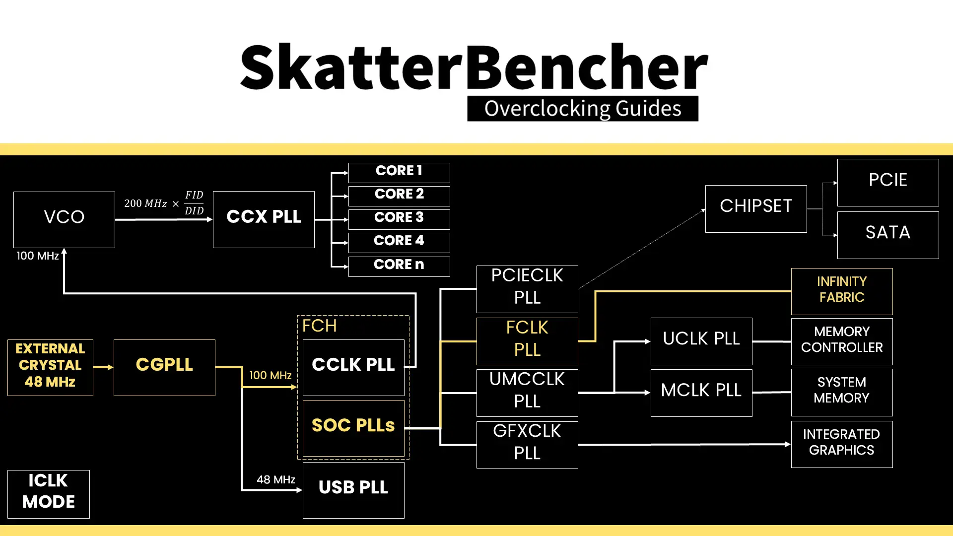
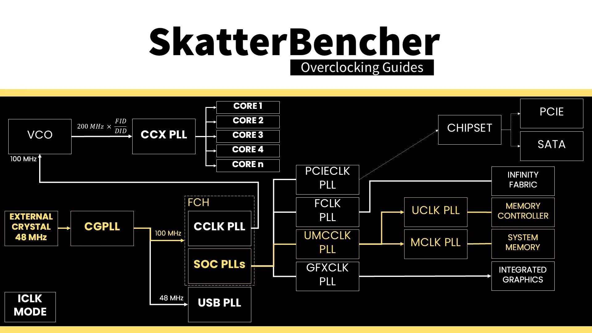
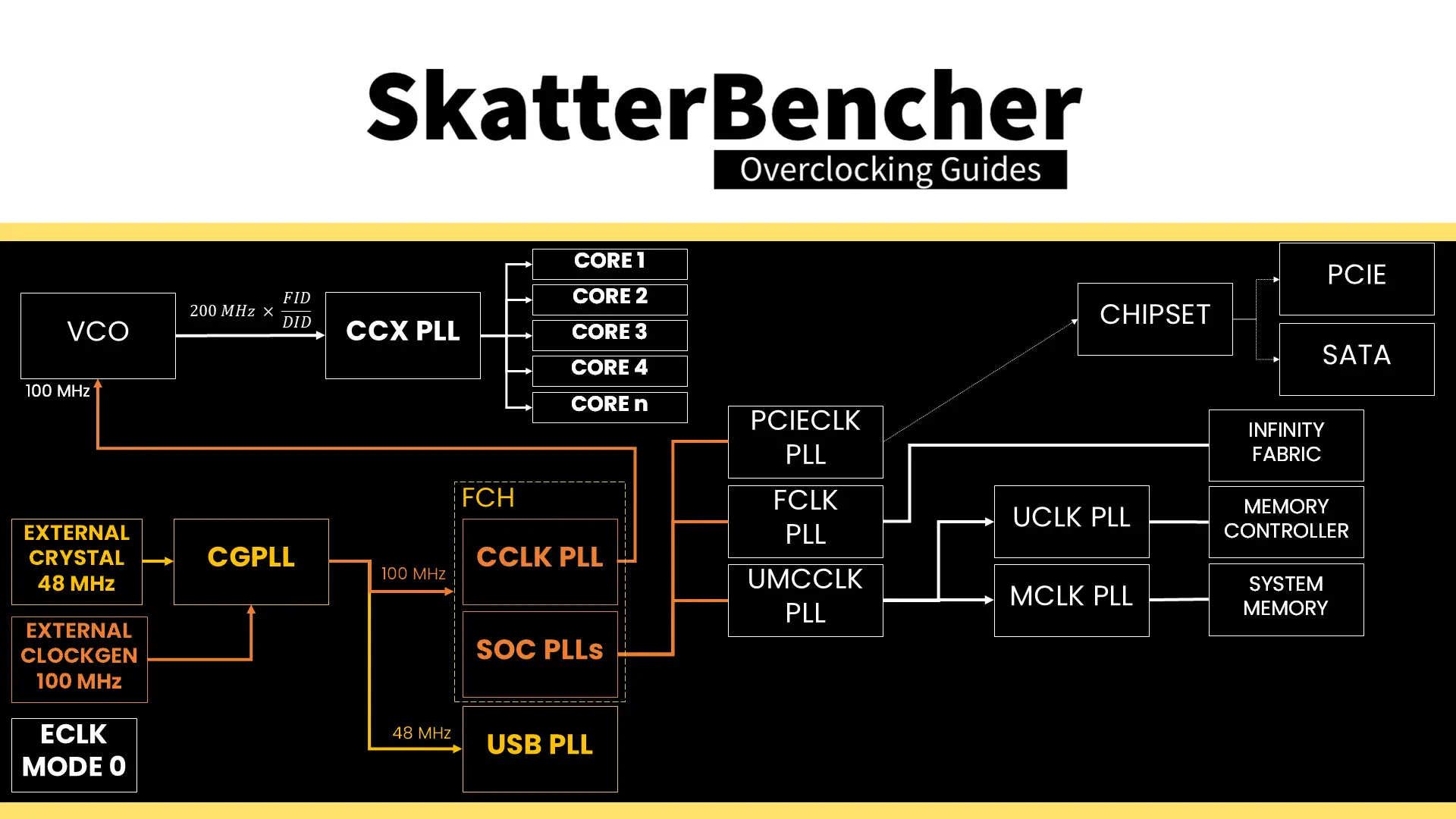
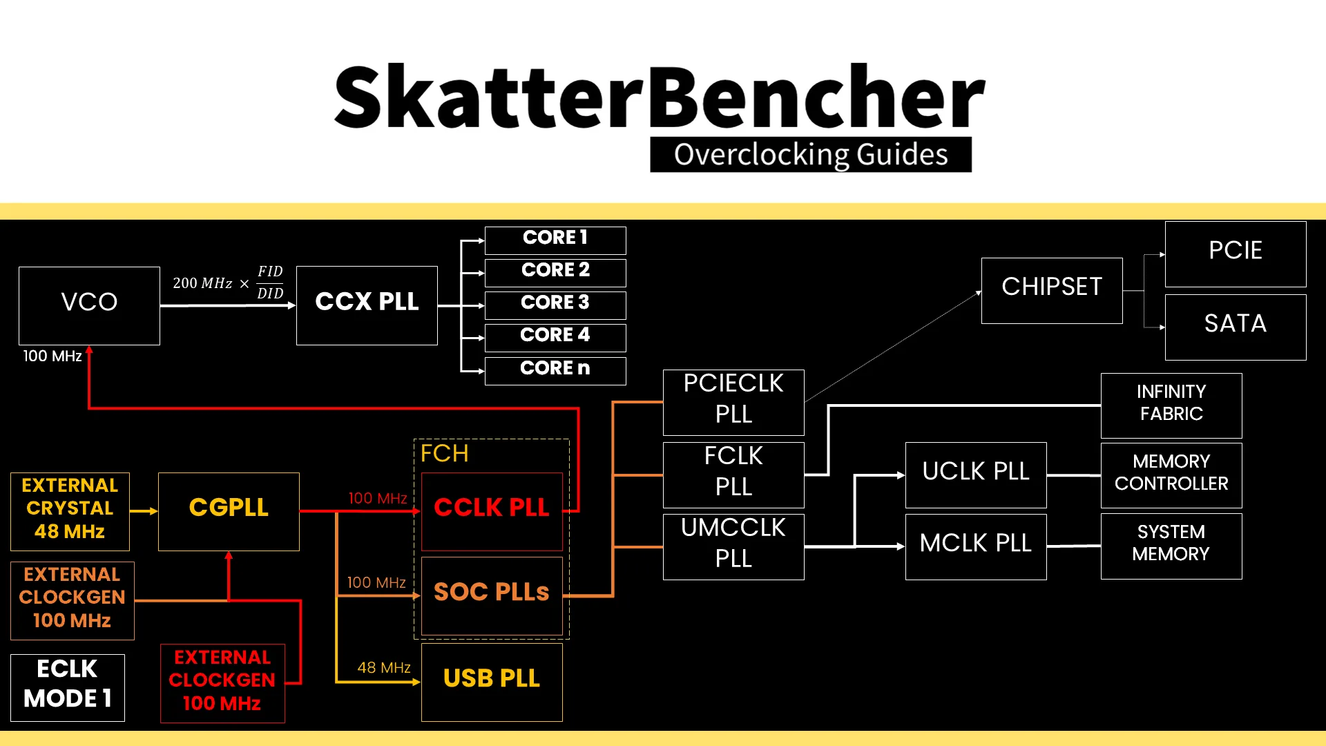
The standard Granite Ridge platform has a 48 MHz crystal input to the integrated CGPLL clock generator. The CGPLL then generates a 48 MHz clock for the USB PLL and a 100 MHz reference clock for the FCH, which contains the CCLK PLL for the CPU cores and several SOC PLLs.
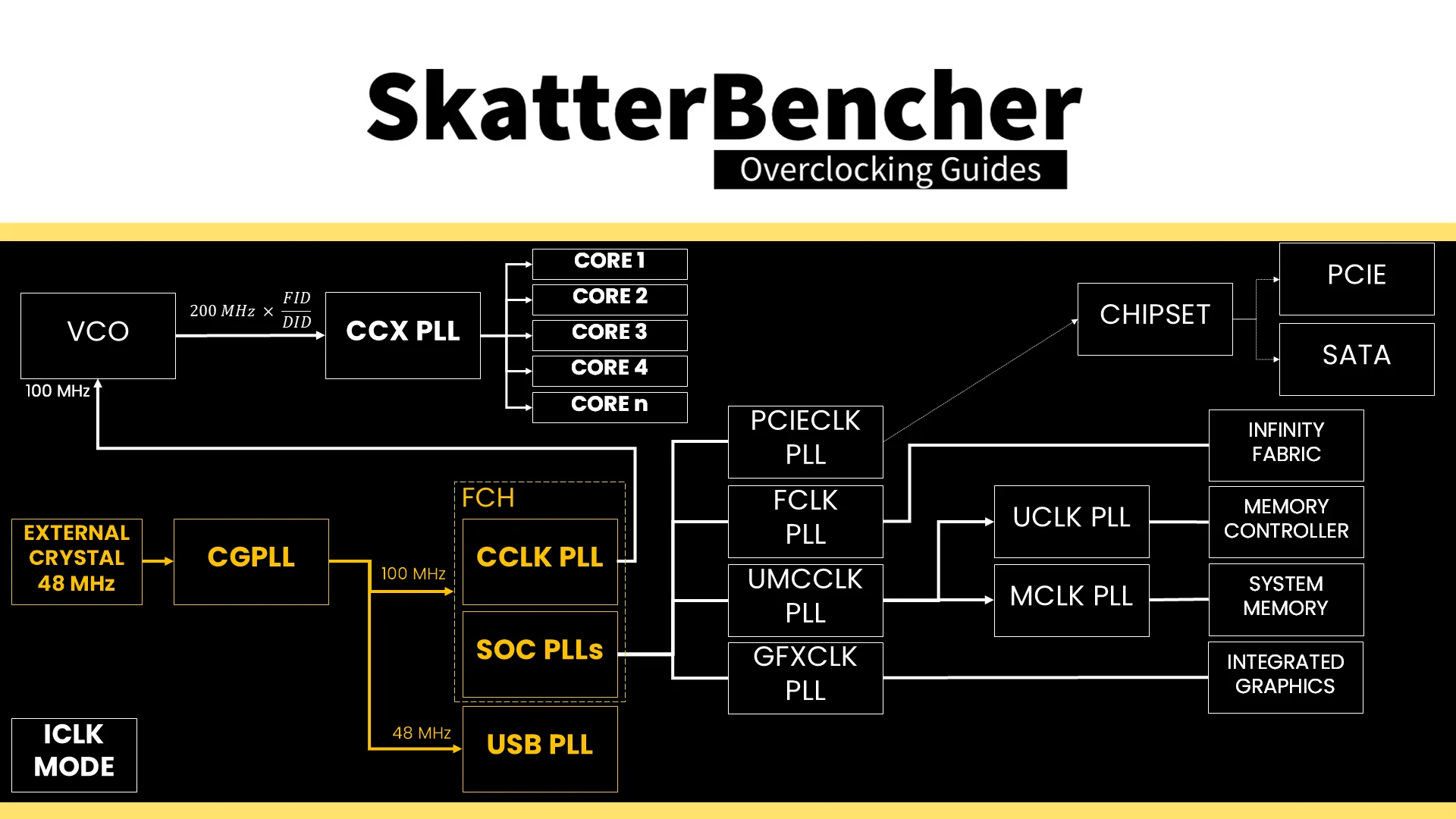
The external clocks are inputs to the FCH. There you can configure how you want to use the external clocks. In addition to the standard internal CGPLL, Granite Ridge supports up to two external clock modes. They’re called eCLK0 Mode and eCLK1 Mode.
- In eCLK0 Mode, an external 100MHz reference clock is used for both the CPU and SOC PLLs. In other words, it’s a reference clock that affects the CPU core clocks and the PCIe and SATA clocks.
- In eCLK1 Mode, there are two distinct external 100MHz reference clocks. One clock provides the 100MHz input for the CPU PLL, and another provides the 100MHz reference clock for the SOC PLLs.
The overclocking strategy with ECLK is the polar opposite of what we’re used to with Ryzen CPUs. OC Strategy #2 shows that Ryzen overclocking is typically done with a negative curve optimizer. That pushes the Precision Boost algorithm to reach higher boost frequencies.
With ECLK, we still build on the factory-fused VFT curve but adjust the frequency by adjusting the reference clock. A key challenge with using ECLK is that we’re applying a linear stretch on a non-linear V/F curve. Let me explain with an example.
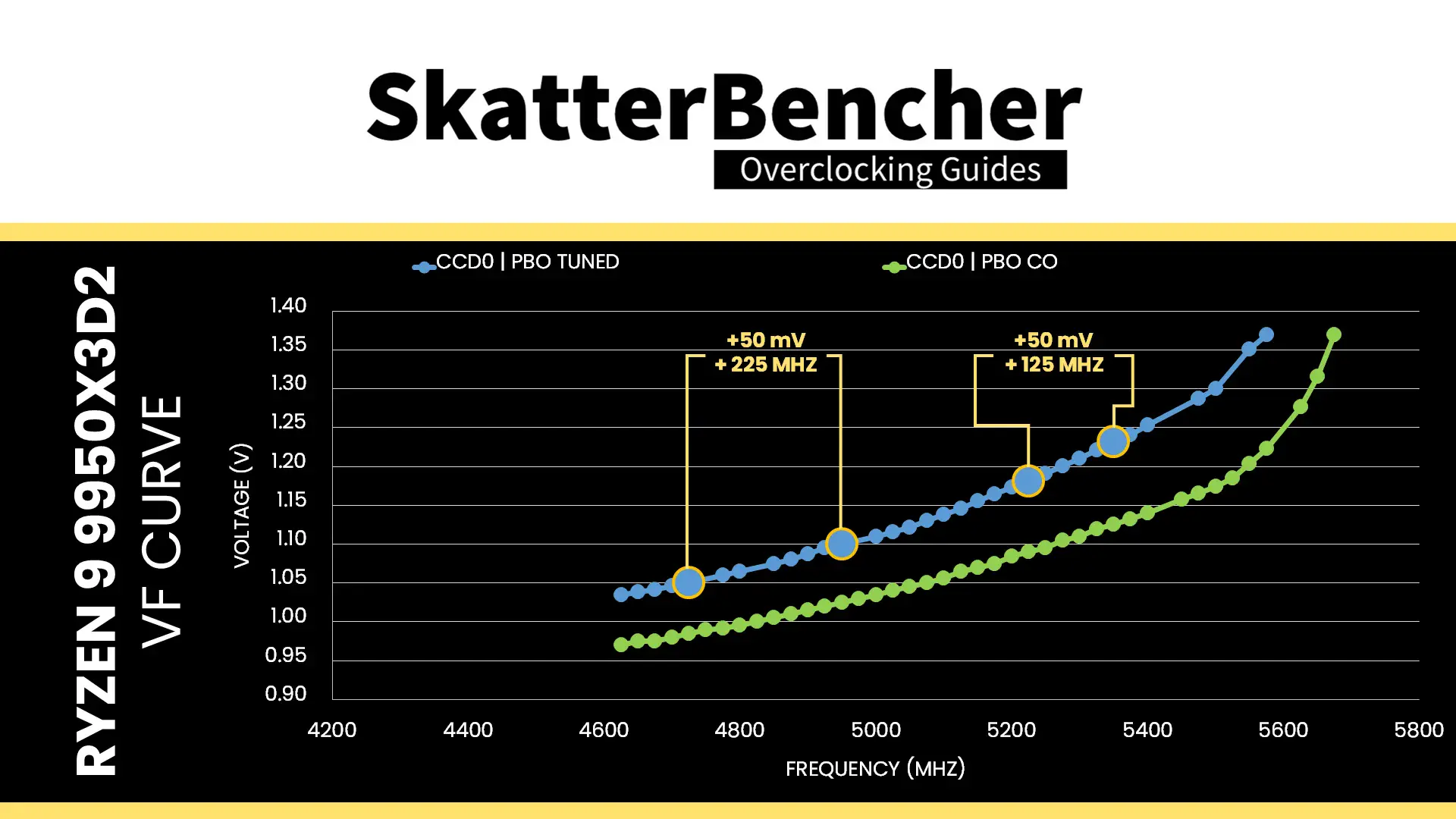
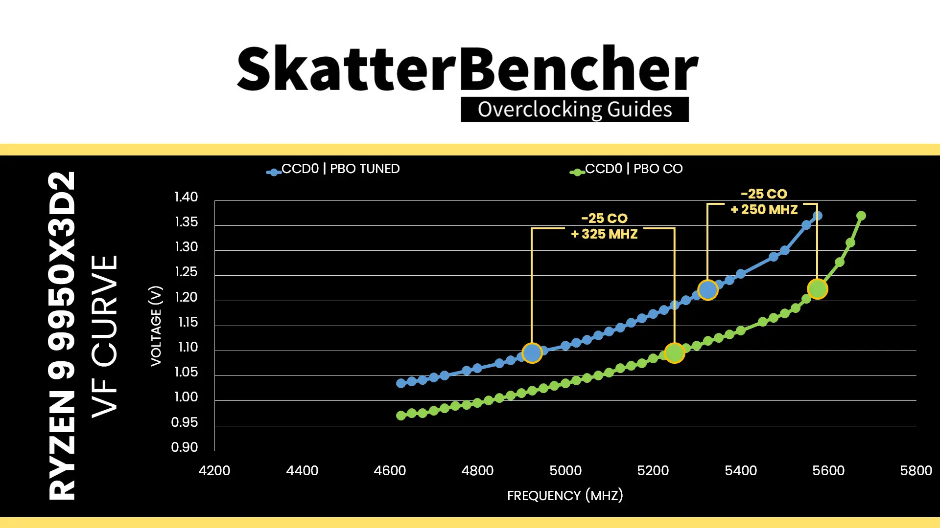
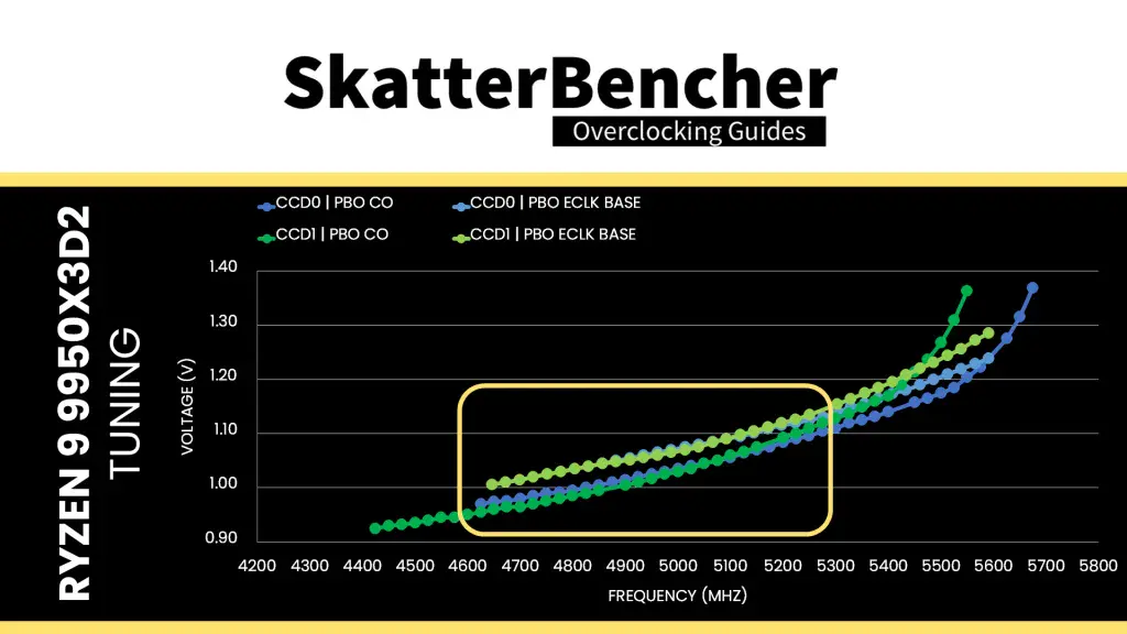
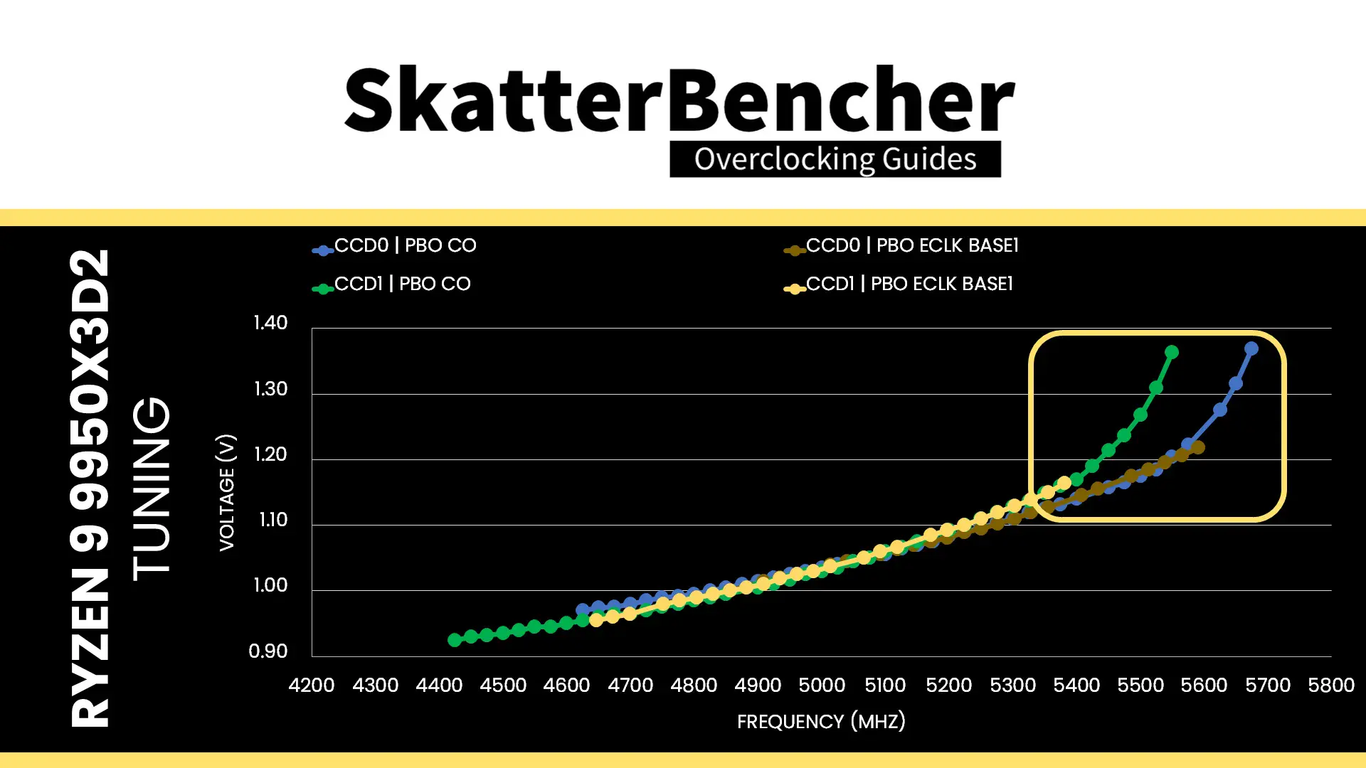
Here you can see four V/F curves of the Ryzen 9 9950X3D2: the default curves and the ones from OC Strategy #2 tuned with Curve Optimizer. We can see the law of diminishing marginal returns: the higher the frequency, the less additional frequency with every step of additional voltage.

Let’s check CCD0, for example. On the default curve, increasing the voltage 50mV from 1.05V to 1.10V gives an extra 225 MHz (4950-4725), but increasing from 1.181V to 1.232V (also 50mV) only gives an extra 125 MHz (5350-5225). The law of diminishing returns also applies to our undervolt. With a -25 curve optimizer we get an extra 325 MHz at 1.095V (5250-4925) but only +250 MHz at 1.22V (5575-5325).
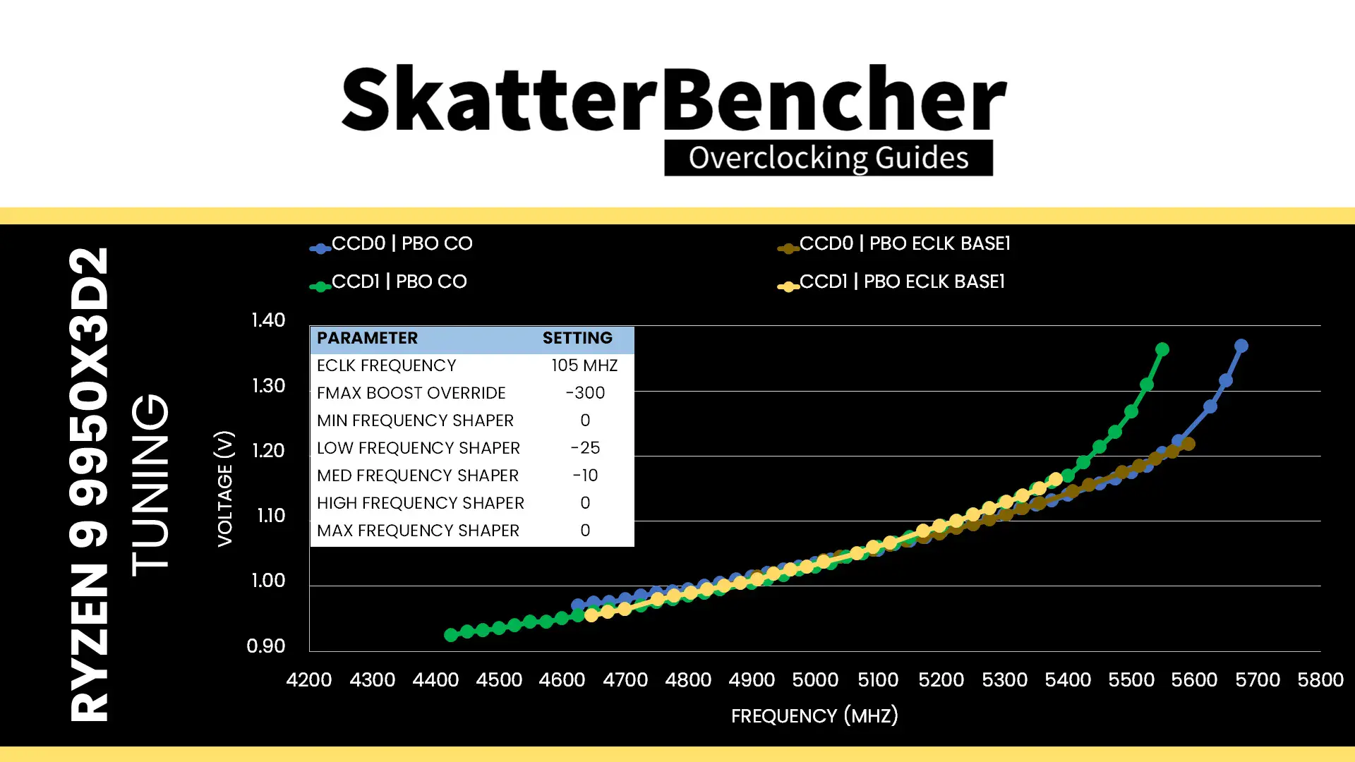
We can simulate the V/F curves with adjusted eCLK by multiplying the stock V/F curve with our target eCLK frequency. For example, if we were to increase the ECLK by 5%, setting it to 105 MHz, then the resulting curves would look as follows.
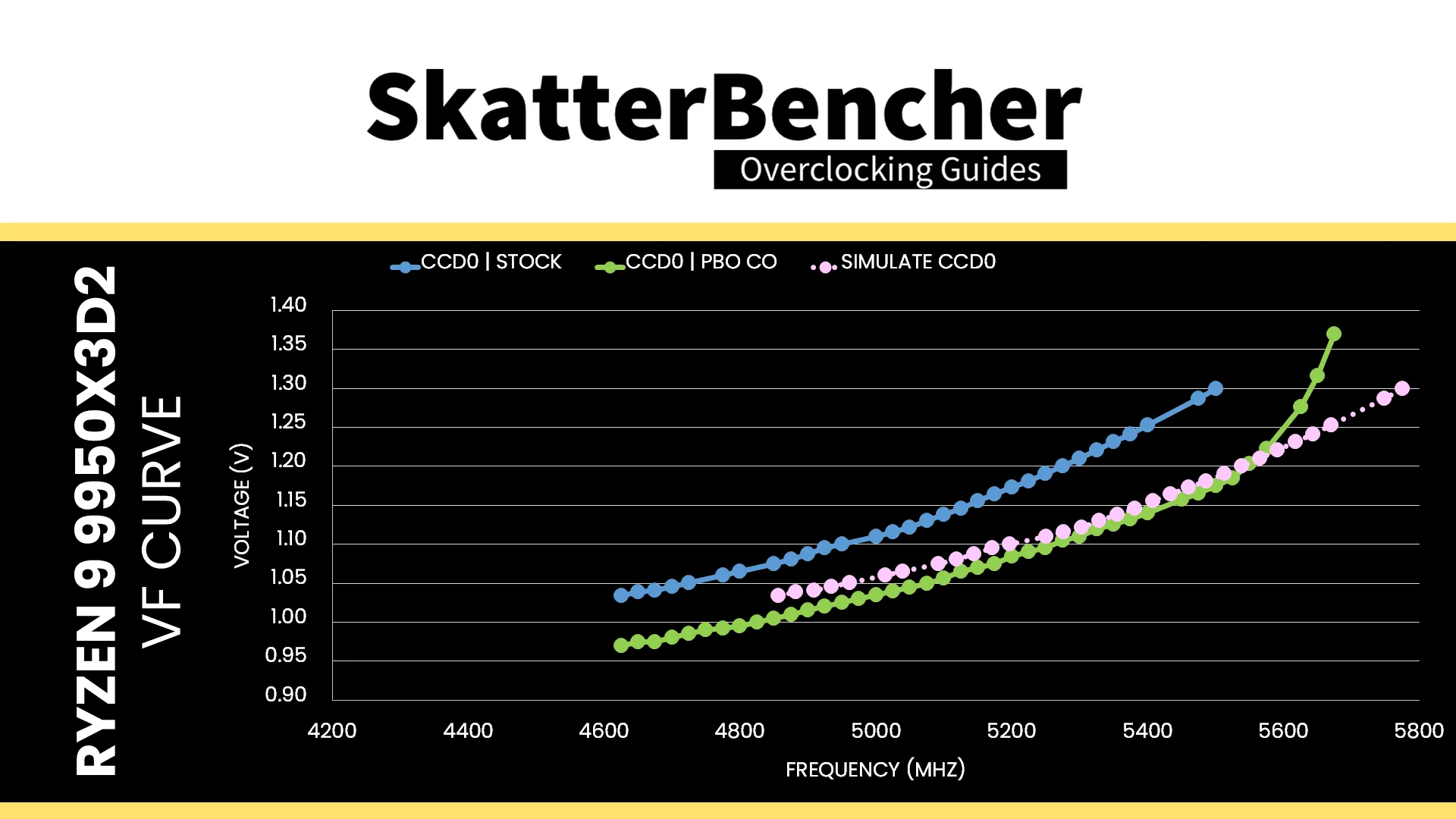
We can make two key observations:
- The frequency increases by 220 to 280 MHz across the entire curve and doesn’t show any diminishing returns.
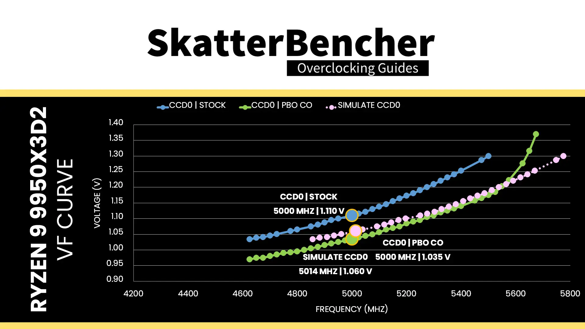
- While the voltage for a given frequency is lower than the default curve, it is higher than with our Curve Optimized curve. For example, on CCD0, for 5 GHz we need 1.110V by default, about 1.060V when using 105 MHz ECLK, but only 1.035V when Curve Optimized.
Here’s what the actual V/F curves looks like with 105 MHz ECLK. You can see it’s pretty close to our simulated curve.
Note that I did have to set the Fmax boost override to -300 for CCD0 and -100 for CCD1 because the peak boost frequencies were unstable.
Before Ryzen 9000, we could only rely on Curve Optimizer to tune the curve. That meant we could use a positive Curve Optimizer to squeeze higher frequency at the upper end of the curve by sacrificing frequency (and thus performance) at the lower end of the curve.
However, with Ryzen 9000 CPUs we have a critical new tool in the overclocking toolbox: Curve Shaper.
Curve Shaper
Curve Shaper is the newly introduced tool of the Precision Boost Overdrive 2 toolkit. It was introduced alongside the Zen 5 Ryzen 9000 “Granite Ridge” processors. I had an in-depth look at the tool in a different guide on this website.

In theory, it seems Curve Shaper is pretty straightforward: you get fifteen additional tunable points across the V/F curve. But the devil is in the details because AMD’s Precision Boost 2 technology doesn’t really work with V/F points. So, instead of getting a list of specific tunable V/F points, we get five frequency regions and three temperatures:
Frequency Regions:
- Minimum frequency (“idle”)
- Low frequency (“background tasks”)
- Medium frequency (“high core count workloads”)
- High frequency (“gaming workloads”)
- Max frequency (“1T workloads”)
Temperatures:
- Low temperature (“idle”) = -5°C
- Medium temperature (“1T gaming workloads”) = 50°C
- High temperature (“stress test workloads”) = 90°C
The regions have a bit of a vague terminology and are not clearly defined. I will get back to that in a minute. The temperature points are more straightforward as they’re defined as -5, 50, and 90 degrees Celsius.
The idea of Curve Shaper is that you can adjust the voltage-frequency curve in more specific areas than with Curve Optimizer. For example, you could say that you only want to undervolt in the High Frequency region for temperatures between 50 to 90 degrees Celsius. That would be a common approach to increase the operating frequency in gaming workloads.
In our case, we want to use Curve Shaper for two reasons:
- Constrain the undervolt in the peak frequency region to stabilize the max frequency targets.
- Explore additional undervolting opportunities for all-core workloads.
For the first objective, we can use Curve Shaper values for high and maximum frequency regions. For the second objective, we can use negative Curve Shaper values for low and medium frequency regions.
Let’s get a bit more practical with the process.
Ryzen 9 9950X3D2 Curve Shaper Tuning Process
Similar to Curve Optimizer, the manual tuning process for Curve Shaper can become quite convoluted since it affects the CPU core stability in all scenarios ranging from very light single-threaded workloads to heavy all-core workloads. A key difference with Curve Optimizer is that Curve Shaper is only available on a Per CPU basis so any tuning will affect every CCD’s V/F curve.
The first goal was to explore clawing back some of the undervolt margin in the lower part of the V/F curve used by heavier all-core workloads. For this purpose, we can use the Low and Medium Frequency Curve Shaper Points. The typical workloads used for stability checking include OCCT, Y-Cruncher, AI Benchmark, and Cinebench.
After a bit of testing, I found that the maximum undervolt was -25 for Low Frequency and -10 for Medium Frequency. The key bottleneck was Y-Cruncher stability.
The new V/F curves look strikingly similar to the Curve Optimized curves from OC Strategy #2. That’s relatively good news as it means that, likely, we also maximized the performance in OC Strategy #2.
The second goal was to maximize our peak boost frequency for which we can use the High and Max Frequency Curve Shaper points as well as the Fmax Boost Override. We already know we’ll need a positive magnitude for the Curve Shaper points because we needed to set a negative Fmax Boost Override to prevent CPU instabilities after increasing the eCLK to 105 MHz.
So, the approach is to set the High Frequency point to +15 and the Max Frequency Point to +30, then gradually increase the Fmax Boost Override until we either see signs of instability or the boost frequency stops increasing due to the 1.4V voltage limit.
The key bottleneck turned out to be Geekbench 6 Single Thread as it would fail to pass the benchmark at high frequency AVX workloads. After a bit of tuning, I found I could set the Fmax Boost Override to 0 (or “disabled’) with those positive shaper points.
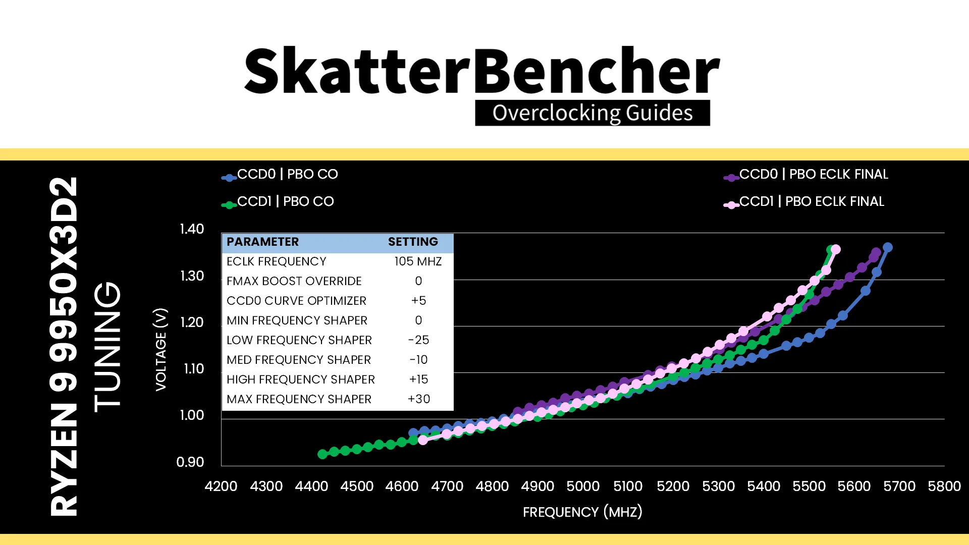
The maximum theoretical boost frequency is therefore 5625 x 1.05 = 5906 MHz for CCD0 and 5425 x 1.05 = 5696 MHz for CCD1. But, as we’ll see in a bit, the actual maximum boost frequency is about 5820 MHz for CCD0 and 5680 MHz for CCD1 due to the voltage limit.
Curve Shaper is a very powerful tuning tool, and this example perfectly captures its core strength: adjusting the under- and overvolt at different parts of the curve which maximizes the frequency in light and heavy workloads.
BIOS Settings & Benchmark Results
Upon entering the BIOS
- Go to the Extreme Tweaker menu
- Set Ai Overclock Tuner to EXPO II
- Set eCLK Mode to Asynchronous mode
- Set BCLK2 Frequency to 105.00
- Set Memory Frequency to DDR5-7800
- Enter the DRAM Timing Control submenu
- Enter the Memory Presets submenu
- Select Load Hynix 7600MHz 1.45V 2x16GB SR and click OK
- Leave the Memory Presets submenu
- Set TREFI to 32767
- Enter the Memory Presets submenu
- Leave the DRAM Timing Control submenu
- Set VDDSOC Voltage Override to Offset
- Set VDDSOC Voltage Offset to 0
- Switch to the Advanced menu
- Enter the AMD Overclocking submenu and click accept
- Enter the DDR and Infinity Fabric Frequency/Timings submenu
- Enter the Infinity Fabric Frequency and Dividers submenu
- Set Infinity Fabric Frequency and Dividers to 2200 MHz
- Leave the Infinity Fabric Frequency and Dividers submenu
- Enter the Infinity Fabric Frequency and Dividers submenu
- Leave the DDR and Infinity Fabric Frequency/Timings submenu
- Enter the Precision Boost Overdrive submenu
- Set Precision Boost Overdrive to AdvancedSet PBO Limits to MotherboardSet Precision Boost Overdrive Scalar Ctrl to Manual
- Set Precision Boost Overdrive Scalar to 10X
- Set Curve Optimizer to Per CCD
- Set CCD 0 Curve Optimizer Sign to PositiveSet CCD 0 Curve Optimizer Sign to 5
- For Low, Medium, High, and Max Frequency, set All Temperature to EnableFor Low and Medium Frequency, set Sign to NegativeFor High and Max Frequency, set Sign to PositiveFor Low Frequency, set Magnitude to 25For Medium Frequency, set Magnitude to 10For Max Frequency, set Magnitude to 30
- Enter the SoC Voltage submenu
- Set SoC Voltage to 1150
- Set Precision Boost Overdrive to AdvancedSet PBO Limits to MotherboardSet Precision Boost Overdrive Scalar Ctrl to Manual
- Enter the DDR and Infinity Fabric Frequency/Timings submenu
Then save and exit the BIOS.
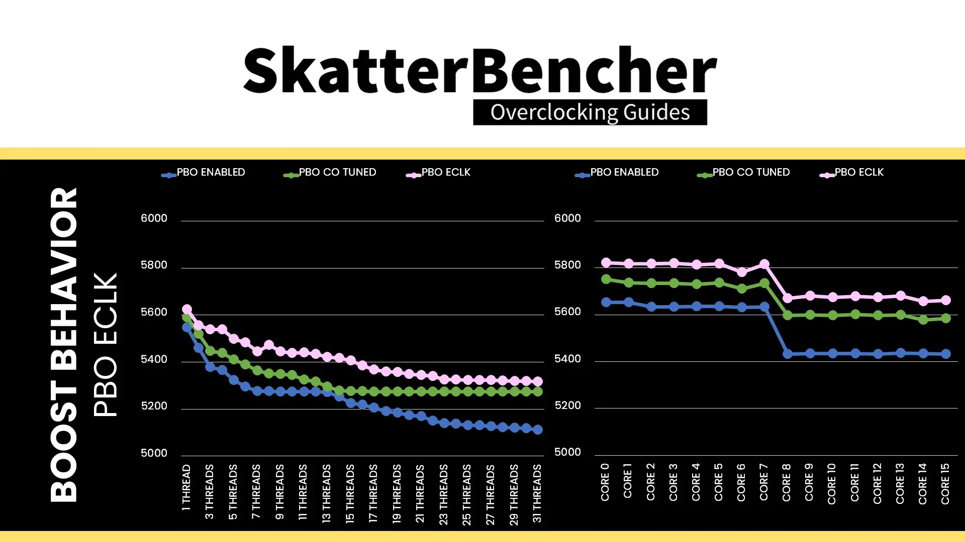
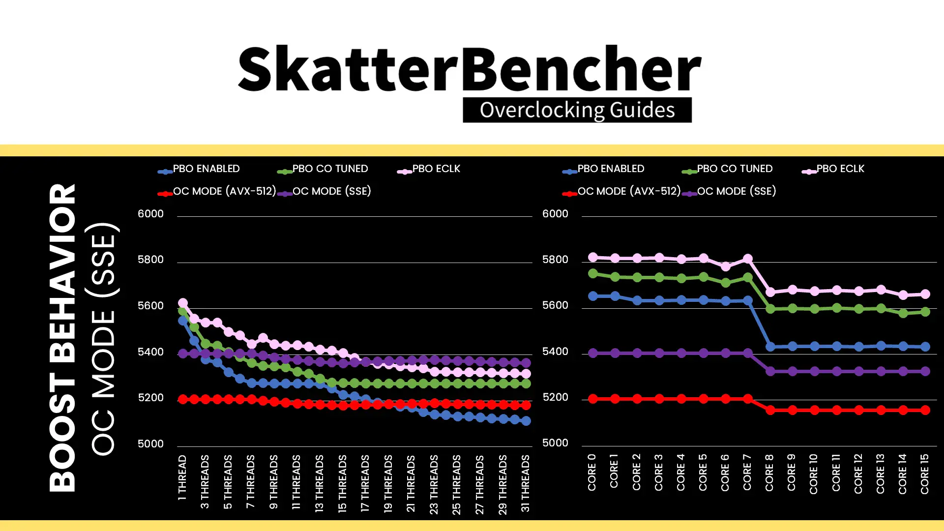
The boost frequency at 1 active thread is about 5624 MHZ and the average boost frequency gradually trails off to 5316 MHz when all cores are active. In light single-threaded workloads, seven of the eight cores in CCD0 can boost to over 5.8 GHz and all cores in CDD1 to over 5.6 GHz.
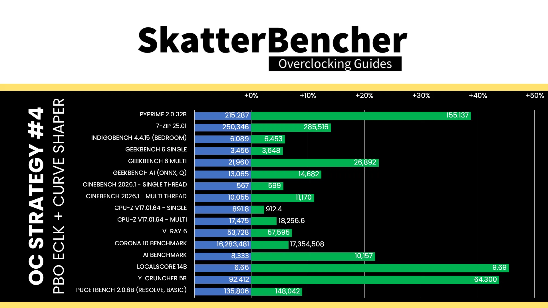
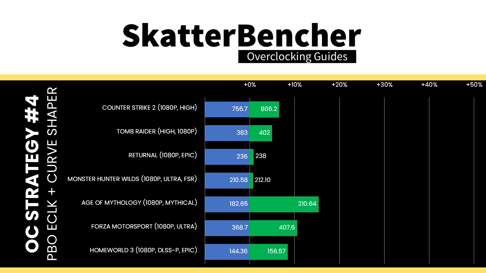
We re-ran the benchmarks and checked the performance increase compared to the default operation.
Asynchronous eCLK is a hardcore way of squeezing more performance out of the Precision Boost 2 algorithm and while it didn’t yield substantially higher frequencies, we do see meaningful performance uplift. The geomean performance speedup improves by one percentage point, and we get a maximum benchmark speedup of +45.50% in LocalScore.
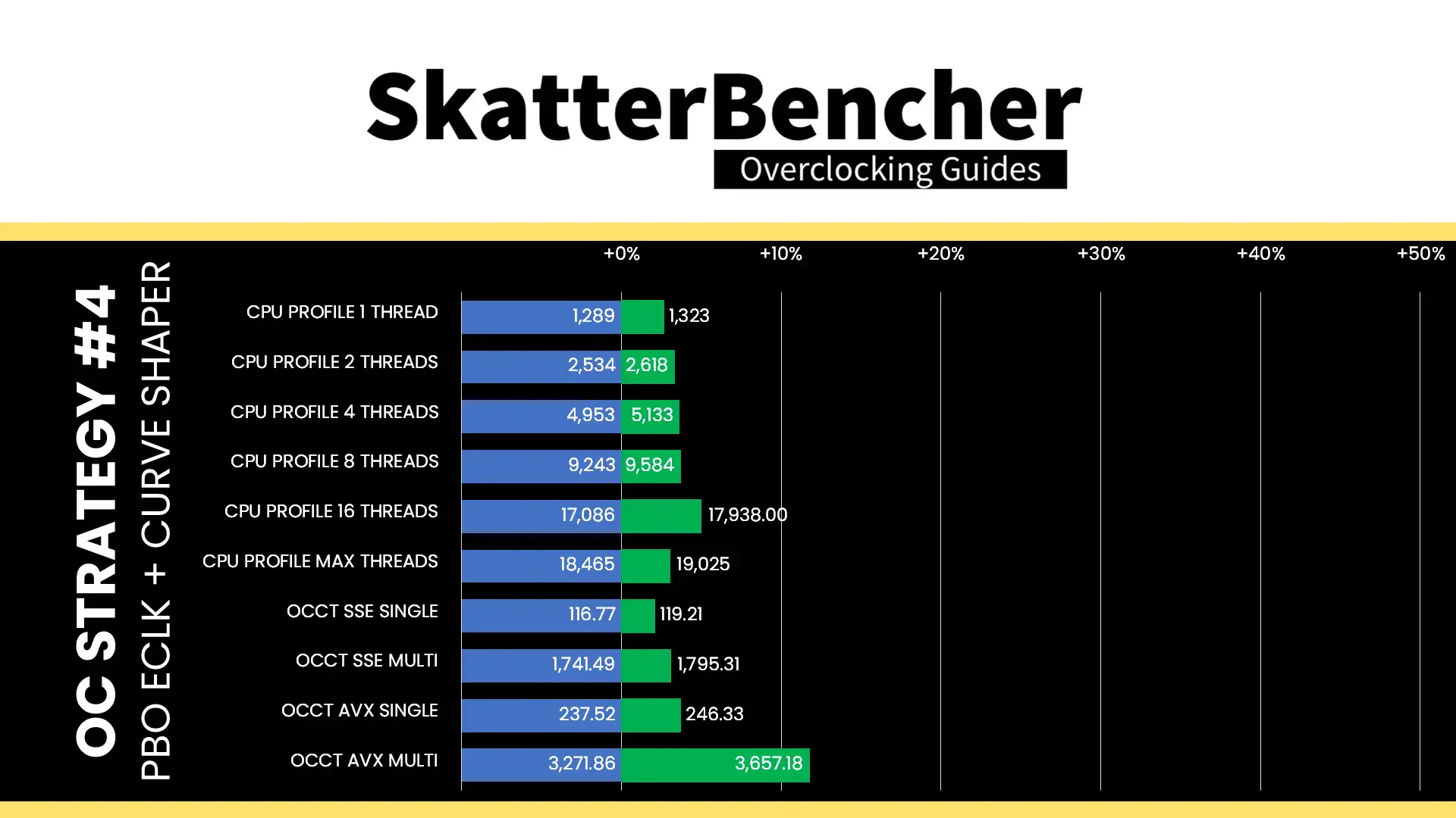

When running the OCCT CPU AVX-512 Stability Test, the average CPU CCD0 effective clock is 4869 MHz and CCD1 effective clock is 4769 MHz with 1.073 volts. The average CPU temperature is 83.7 degrees Celsius. The average CPU package power is 258.0 watts.
When running the OCCT CPU SSE Stability Test, the average CPU CCD0 effective clock is 5267 MHz and CCD1 effective clock is 5226 MHz with 1.235 volts. The average CPU temperature is 93.5 degrees Celsius. The average CPU package power is 310.8 watts.

OC Strategy #5A: OC Mode (Part 1)
In our final overclocking strategy, we will pursue a manual overclock.
One could question the use-case for manual overclocking an AMD Ryzen CPU. Just like with all past Ryzen processors, the major downside of manual overclocking is that you lose the benefits of Precision Boost technology in low-threaded benchmark applications. So, whereas this Ryzen 9 9950X3D2 can boost up to 5625 MHz with Precision Boost, it will be limited to your set fixed frequency when manually overclocking.
However, manual overclocking is not all negative and even has a couple of benefits.
- First, it’s much simpler and usually faster than tuning with the advanced overclocking tools from the Precision Boost Overdrive 2 toolkit like Curve Optimizer
- Second, automatic overclocking and frequency boosting technologies can leave a little margin on the table. We can exploit this margin and fine-tune it for application stability when manually overclocking with our specific hardware configuration.
- Lastly, sometimes the static voltage and frequency configuration runs cooler than using a dynamic, adaptive clocking technology.
To better understand the performance tuning opportunities embedded in the Ryzen 9 9950X3D2 processor, let’s look at its clocking and voltage topology in more detail.
Ryzen 9000 CPU Core Clocking Topology
The standard Granite Ridge platform has a 48 MHz crystal input to the integrated CGPLL clock generator. The CGPLL then generates a 48 MHz clock for the USB PLL and a 100 MHz reference clock for the FCH, which contains the CCLK PLL for the CPU cores and several SOC PLLs.
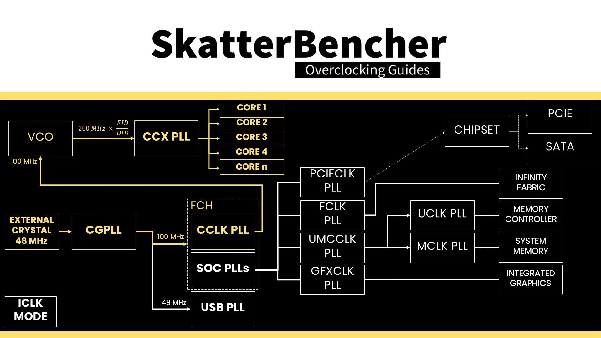
The CCLK PLL 100MHz reference clock drives the 200 MHz VCO, which is then multiplied by an FID and divided by a DID. This used to provide us with a 25 MHz clock granularity, but with Granite Ridge processors we can now set the frequency in steps of 5 MHz or 0.05X!
Each CCX has its own PLL, with the cores within that CCX running at the same frequency. In a typical operation, all cores within a CCX will run at the same frequency. The effective clock will differ if the core is in a different P-state.
When we switch to OC Mode, we disable all automatic Precision Boost frequency boosting technologies and rely solely on the manual frequency and voltage configuration.
Ryzen 9000 CPU Core Voltage Topology
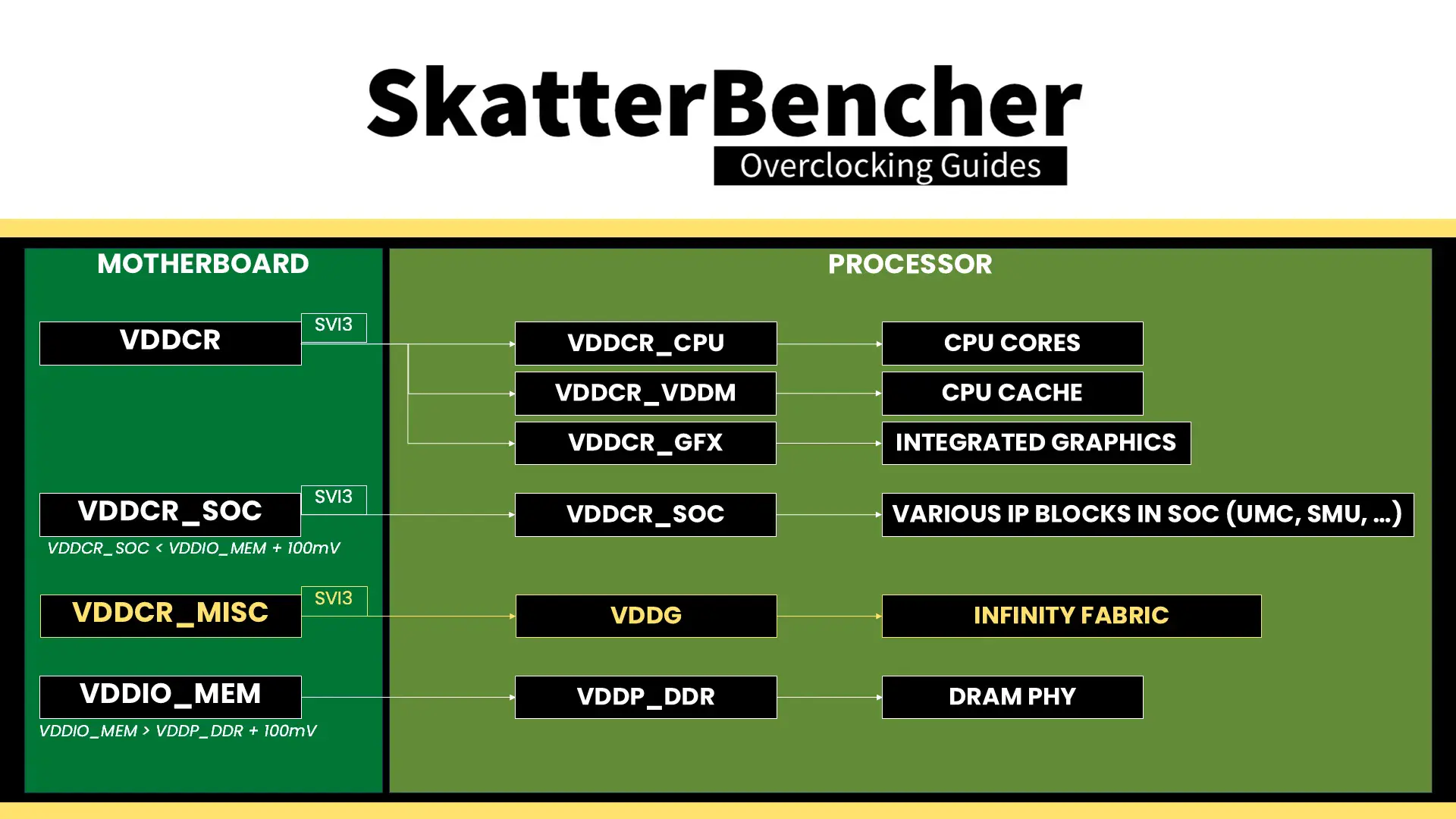
The Ryzen 9000 voltage topology relies on a combination of internal and external power supply to generate the processor voltages.
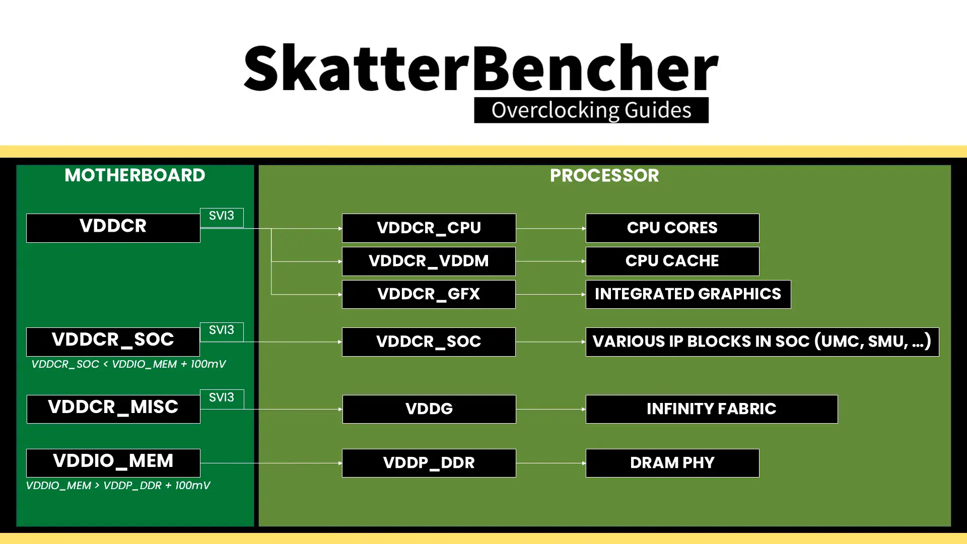
There are four primary power supplies from the motherboard VRM to the processor: VDDCR, VDDCR_SOC, VDDCR_MISC, and VDDIO_MEM_S3. The VDDCR voltage rail provides external power for three internal voltage regulators: VDDCR_CPU, VDDCR_VDDM, and VDDCR_GFX.
- VDDCR_CPU provides the voltage for the CPU cores in CCX. The voltage rail can work in either regular or bypass mode, but on Granite Ridge, it is always in bypass mode. That means the voltage is always equal to the VDDCR external voltage.
- VDDCR_VDDM provides the voltage for the L2, L3, and, if present, 3D V-Cache on a CCX. This rail cannot work in bypass mode; therefore, it is internally regulated from the VDDCR external voltage rail. The default VDDM voltage is 0.95V
- VDDCR_GFX provides the voltage for the integrated graphics.
The VDDCR voltage rail is directly controlled by the CPU SMU using an SVI3 interface. On this motherboard, we can configure this voltage regulator in the BIOS. A crucial parameter is the VRM load line setting.
VRM load line
The VRM load line is essential for two reasons: the Vdroop and undershoot.
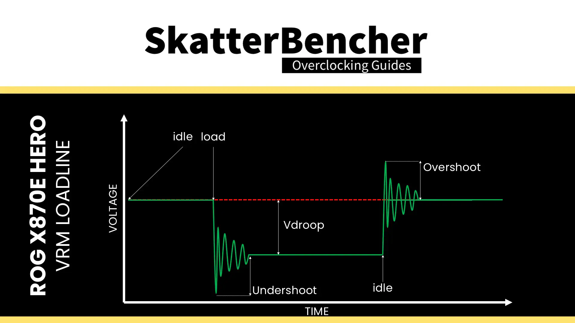
Vdroop is the decrease in voltage when the CPU goes from idle to load. You want your CPU to be stable in all scenarios, so knowing the lowest voltage the CPU runs at is very important. After all, if the voltage is too low, the overclock won’t be stable.
Undershoot and its counterpart, overshoot, is a brief voltage spike that occurs when the CPU switches from idle to load or from load to idle. These spikes cannot be measured easily and usually require an expensive oscilloscope to detect. I highly recommend the ElmorLabs article titled VRM Load-Line Visualized to see a great picture of undershoot and overshoot in action.
While undershoot and overshoot are temporary spikes, an undershoot that’s too low can cause instability.
The VRM load line setting is relevant to this overclocking strategy because we’re switching from Precision Boost to OC Mode. That means the CPU is no longer regulating the load line itself and instead we have to correctly configure it by ourselves.
Ryzen 9 9950X3D2 CCX Frequency Tuning Process
Choosing the proper manual voltage is always a matter of finding a suitable trade-off between increased overclocking potential, the thermal challenges that come with increased voltage, and of course, consideration of CPU lifespan. With that last thought, we kick off our manual overclocking process.
Our limiting factor will ultimately be the cooling solution as power consumption increases exponentially with operating voltage and temperature scales (somewhat) linearly with power consumption. The maximum voltage will be determined by the application we’re tuning for. So, the first step in our tuning process would be deciding on the stress test representing our worst-case scenario. In this case, I picked the 30 min OCCT AVX-512 CPU Stability Test.
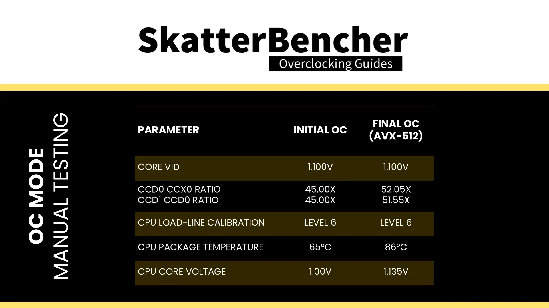
The next step is to set a fixed CPU ratio and check the maximum temperature when running our workload. If there’s thermal headroom left, increase the operating voltage.
For the baseline settings, I look at the OCCT Stress Test results from OC Strategy #2. Here we find that the AVX-512 workload ran at about 4.5 GHz with 1.1V. So, I started the manual tuning process with a CCX ratio of 45X for both CCDs, a VID of 1.1V, and LLC set to Level 6. We find that this gives a temperature of about 65 degrees Celsius and an effective voltage of 1.00V in OCCT AVX-512.
Once we know the maximum voltage, we can tune the CCX ratio. Simply increase the CPU ratio until the application shows instability, then back off. In our case, we end up with the CCD0 Ratio at 52.05X, a CCD1 Ratio at 51.55X, and a Core VID of 1.235V which under high load drops to about 1.135V with Load Line Calibration set to Level 6
BIOS Settings & Benchmark Results
Upon entering the BIOS
- Go to the Extreme Tweaker menu
- Set Ai Overclock Tuner to EXPO II
- Set Memory Frequency to DDR5-7800
- Set FCLK Frequency to 2200 MHz
- Enter the DRAM Timing Control submenu
- Enter the Memory Presets submenu
- Select Load Hynix 7600MHz 1.45V 2x16GB SR and click OK
- Leave the Memory Presets submenu
- Set TREFI to 32767
- Enter the Memory Presets submenu
- Leave the DRAM Timing Control submenu
- Enter the CPU Core Ratio (Per CCX) submenu
- Set CCX0 Ratio to 53.35
- Set CCX1 Ratio to 52.15
- Leave the CPU Core Ratio (Per CCX) submenu
- Enter the DIGI+ VRM submenu
- Set CPU Load-line Calibration to Level 6
- Leave the DIGI+ VRM submenu
- Set Core VID to 1.235
- Set CPU SOC Voltage to Manual Mode
- Set VDDSOC Voltage Override to 1.150
Then save and exit the BIOS.
The boost frequency at 1 active thread is 5205 MHZ and the average boost frequency gradually trails off to 5179 MHz when all cores are active. In all workloads, all cores in CCD0 run at 5205 MHz and all cores in CCD1 run at 5155 MHz.
We re-ran the benchmarks and checked the performance increase compared to the default operation.
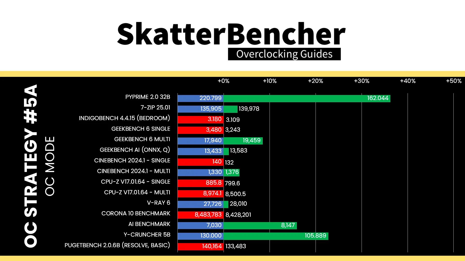
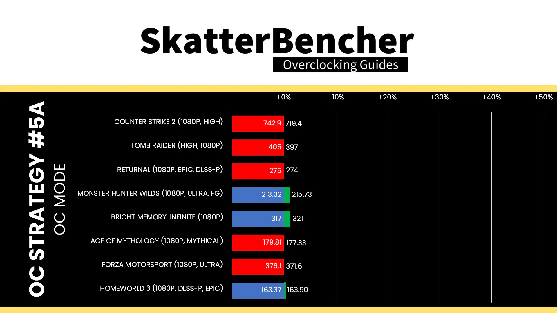
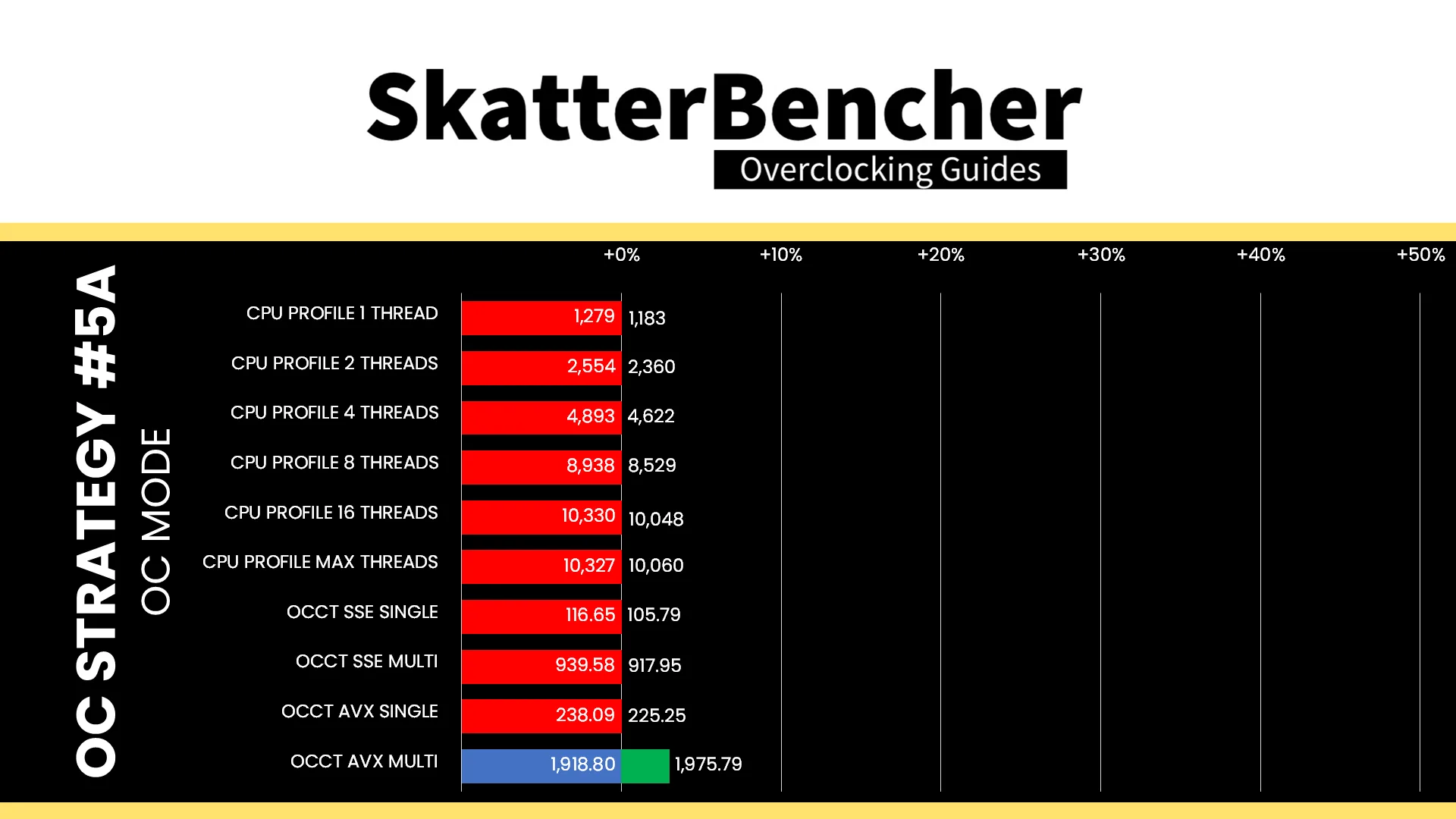

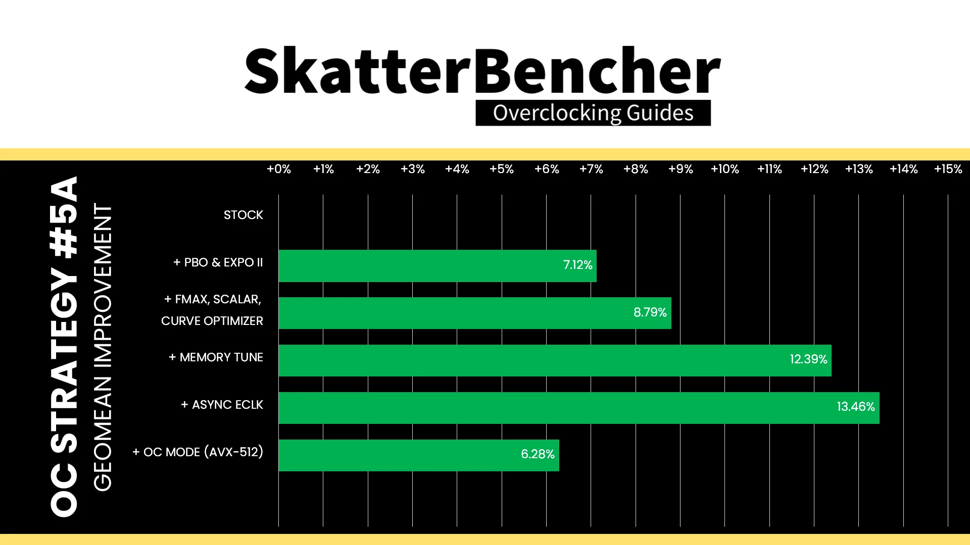
Manually overclocking a Ryzen CPU hasn’t been the path to maximum performance for a while now and the benchmark results show clearly why. Although there are some places where we win over stock configuration, there’s many places where we lose too. The geomean performance speedup over stock is still positive at 6.28%, and we get a maximum benchmark speedup of +45.05% in PyPrime. However, we also see a maximum benchmark slowdown of 16.56% in OCCT AVX Multi.
When running the OCCT CPU AVX-512 Stability Test, the average CPU CCD0 effective clock is 5205 MHz and CCD1 effective clock is 5154 MHz with 1.135 volts. The average CPU temperature is 86.0 degrees Celsius. The average CPU package power is 275.2 watts.

When running the OCCT CPU SSE Stability Test, the average CPU CCD0 effective clock is 5205 MHz and CCD1 effective clock is 5154 MHz with 1.133 volts. The average CPU temperature is 85.2 degrees Celsius. The average CPU package power is 277.7 watts.

OC Strategy #5B: OC Mode (Part 2)
Obviously picking the AVX-512 stress test is a true worst-case scenario that most users wouldn’t encounter, so for science I also tested the maximum frequency with a simple OCCT SSE stress test.
Here I found the maximum operating voltage also to be 1.235V, which droops to about 1.135V under load but it gives me a higher stable frequency. Now we can clock CCD0 to 5405 MHz and CCD1 to 5325 MHz. Stability is a relative term because not only does it fail the OCCT AVX-512 stress test, but it also fails Cinebench 2026, LocalScore, and Y-Cruncher benchmark. All other benchmarks were fine though, so perhaps it is a somewhat reasonable system for gaming workloads.
BIOS Settings & Benchmark Results
Upon entering the BIOS
- Go to the Extreme Tweaker menu
- Set Ai Overclock Tuner to EXPO II
- Set Memory Frequency to DDR5-7800
- Set FCLK Frequency to 2200 MHz
- Enter the DRAM Timing Control submenu
- Enter the Memory Presets submenu
- Select Load Hynix 7600MHz 1.45V 2x16GB SR and click OK
- Leave the Memory Presets submenu
- Set TREFI to 32767
- Enter the Memory Presets submenu
- Leave the DRAM Timing Control submenu
- Enter the CPU Core Ratio (Per CCX) submenu
- Set CCX0 Ratio to 54.05
- Set CCX1 Ratio to 53.25
- Leave the CPU Core Ratio (Per CCX) submenu
- Enter the DIGI+ VRM submenu
- Set CPU Load-line Calibration to Level 6
- Leave the DIGI+ VRM submenu
- Set Core VID to 1.235
- Set CPU SOC Voltage to Manual Mode
- Set VDDSOC Voltage Override to 1.150
Then save and exit the BIOS.
The boost frequency at 1 active thread is 5405 MHZ and the average boost frequency gradually trails off to 5364 MHz when all cores are active. In all workloads, all cores in CCD0 run at 5405 MHz and all cores in CCD1 run at 5325 MHz.
We re-ran the benchmarks and checked the performance increase compared to the default operation.
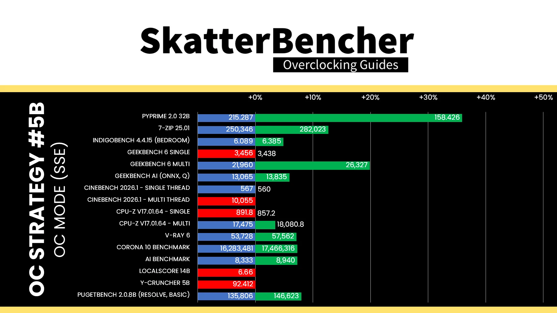
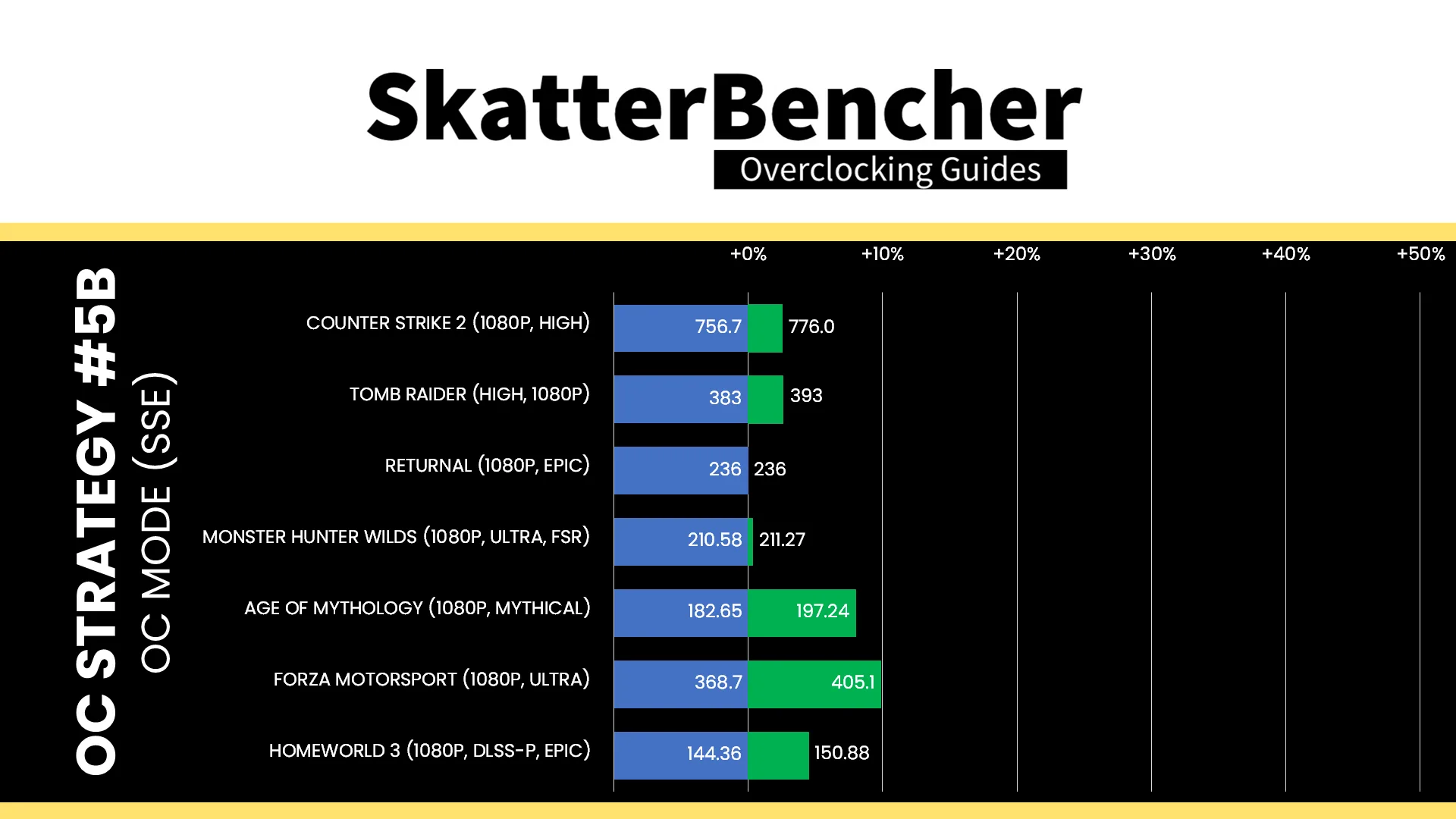
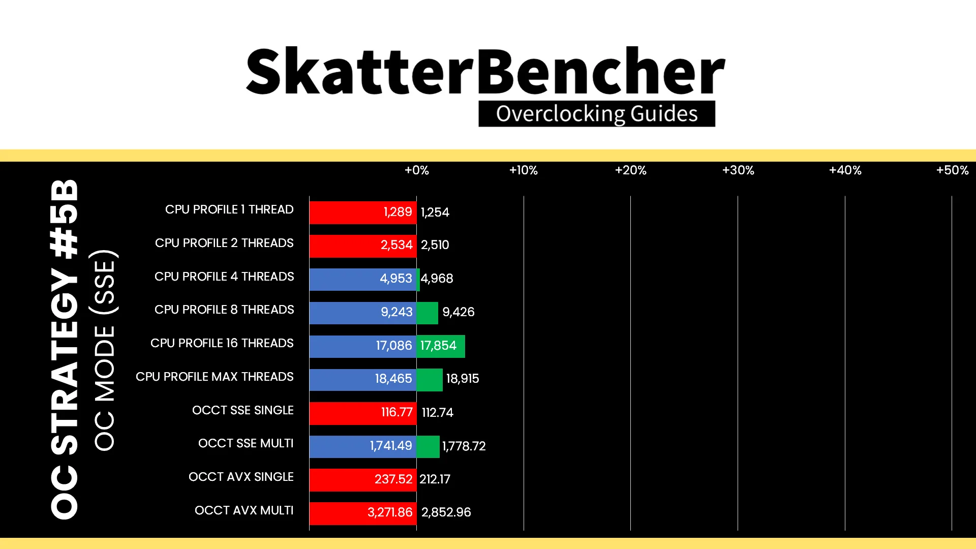

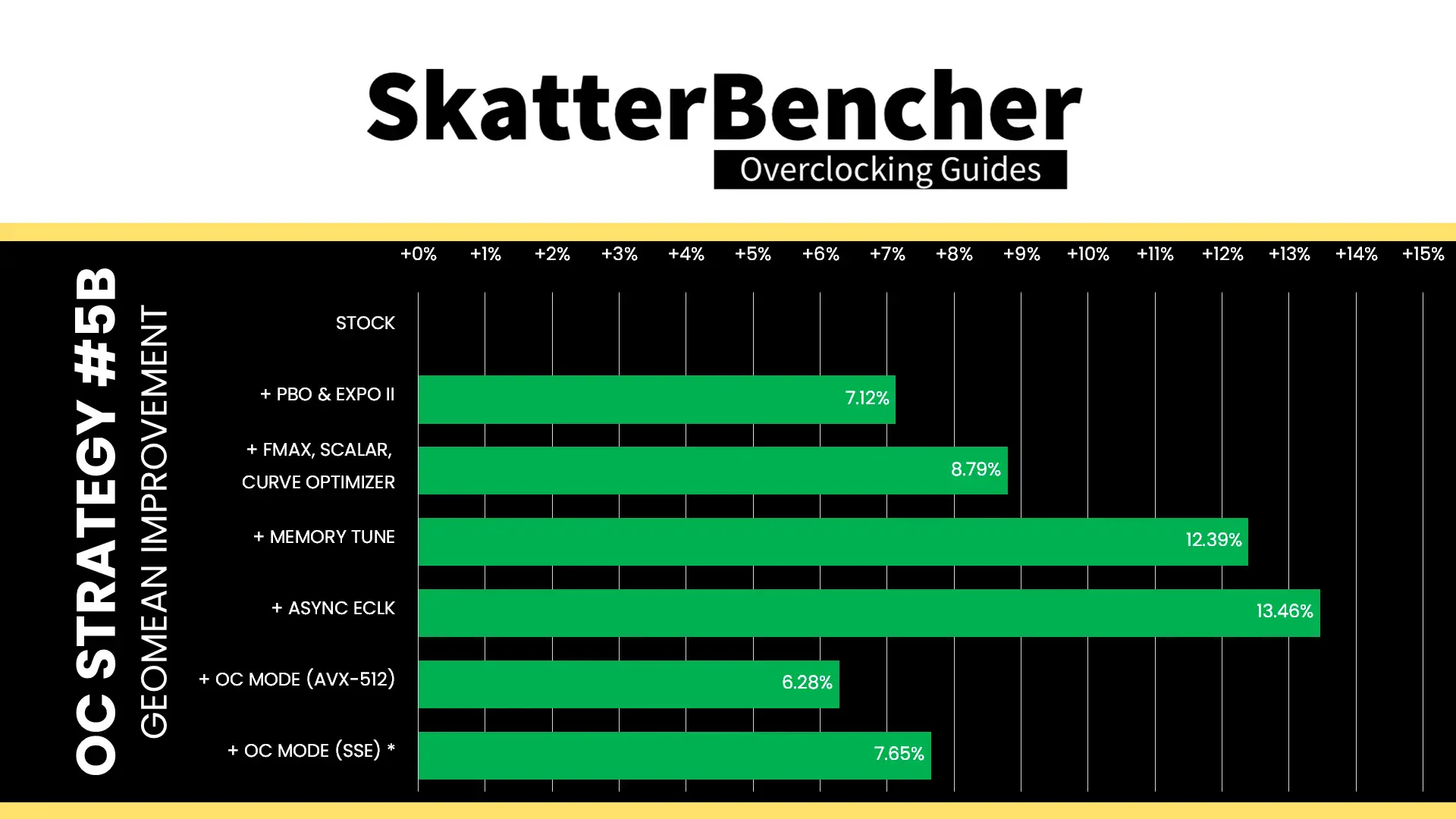
We’re not quite losing out as much as we did in OC Strategy #5A as most benchmarks see a performance bump compared to stock. Yet, we lose against the stock high Precision Boost frequency on eight occasions. The geomean performance speedup over stock is still positive at 7.65%, and we get a maximum benchmark speedup of +35.89% in LocalScore. However, we also see a maximum benchmark slowdown of 12.80% in OCCT AVX Multi.
When running the OCCT CPU SSE Stability Test, the average CPU CCD0 effective clock is 5405 MHz and CCD1 effective clock is 5325 MHz with 1.135 volts. The average CPU temperature is 86.9 degrees Celsius. The average CPU package power is 274.2 watts.
AMD Ryzen 9 9950X3D2: Conclusion
Alright, let’s wrap this up.
I love that AMD decided to go all out and deliver what enthusiasts have been asking for for a while: a dual-X3D product. It’s surprisingly fast in workloads like LocalScore and Y-Cruncher, and somehow, despite the massive L3 cache, also seems to benefit quite well from a high-speed memory subsystem.
Also, we take it for granted now that the X3Ds are overclockable but we must remember that wasn’t the case when the technology first came to market. We are lucky there’s engineers at AMD dedicated to delivering value to the DIY enthusiast market and ensuring not only the dual-X3D can be overclocked, but it comes with all the tuning tools available for every Ryzen 9000 CPU.
Anyway, that’s it for today.
I want to thank my Patreon supporters and YouTube members for supporting my work. If you have any questions or comments, please drop them in the comment section below.
See you next time!
Jamir Reid
Very helpful breakdown of key ideas.