SkatterBencher #84: Core Ultra 9 285K Overclocked to 5800 MHz
We overclock and undervolt the Intel Core Ultra 9 285K to 5800 MHz with the ASUS ROG Maximus Z890 Apex motherboard and custom loop liquid cooling.
We do this by exploring several of the Arrow Lake overclocking tools which I previously covered on this blog. This is probably the most extensive tuning I’ve done, ever.
In this guide, I break down the Core Ultra 9 285K tuning process into six unique overclocking strategies for beginner and advanced overclockers.
- First, we enable ASUS Advanced OC Profile, ASUS MCE, and Intel XMP.
- Second, we do a basic tune of the CPU Cores with Turbo Ratio Limit.
- Third, we optimize the memory subsystem.
- Fourth, we maximize the CPU core overclock by overriding the voltage limits and leveraging OCTVB
- Fifth, we tune the DRAM timings.
- Lastly, we switch to Power Gate mode to see if it makes a real-world difference.
It’s only my second Arrow Lake overclocking guide, so I wasn’t quite sure how to cover as much as possible without taking too much of your time. I suspect this will be a very long video, so please bear with me.
Anyway, before we jump into overclocking, let us quickly review our system, the benchmarks, and the stock performance.
Intel Core Ultra 9 285K: Introduction
The Intel Core Ultra 9 285K is part of Intel’s Core Ultra 200S product line codenamed “Arrow Lake.” The Arrow Lake desktop processors for enthusiasts were introduced on October 24, 2024.
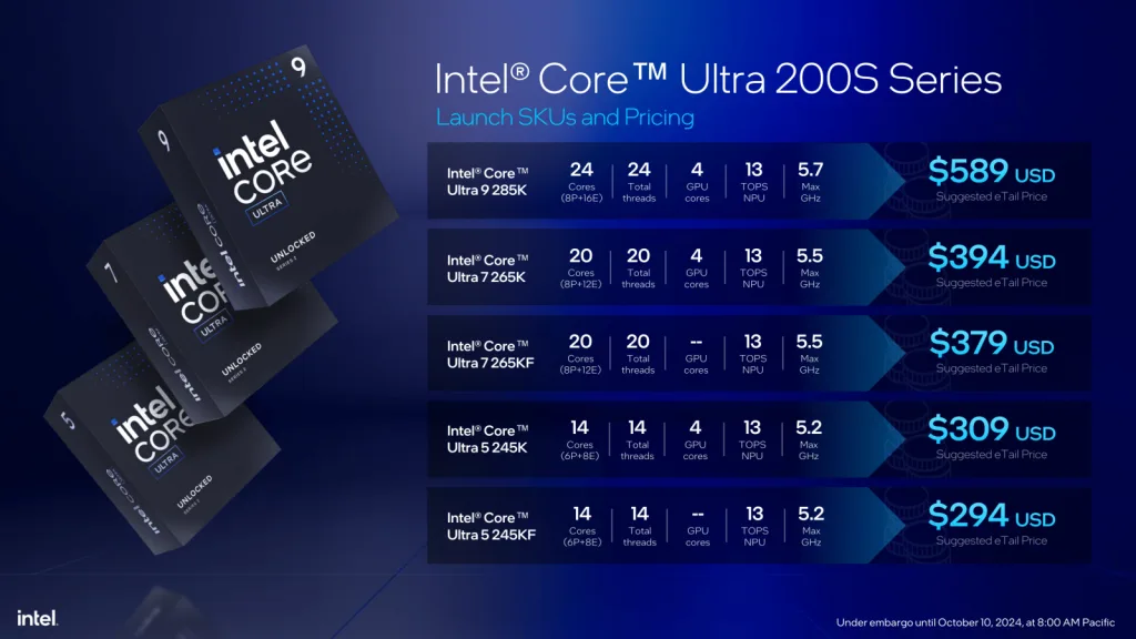
The Core Ultra 9 285K succeeds the 24-core Raptor Lake Core i9-14900K which we overclocked in SkatterBencher #67. It has a P-core base clock of 3.7 GHz and a listed boost frequency of up to 5.7 GHz. The E-cores can boost up to 4.6 GHz. The maximum rated power is 250W.
Platform Overview
The system we’re overclocking today consists of the following hardware.
| Item | SKU | Price (USD) |
| CPU | Intel Core Ultra 9 285K | 640 |
| Motherboard | ASUS ROG Maximus Z890 Apex | 714 |
| CPU Cooling | EK-Quantum Velocity2 EK-Quantum Kinetic FLT 240 D5 EK-Quantum Surface P480M – Black EK-Furious Meltemi 120 (x4) | 150 240 150 |
| Memory | G.SKILL Trident Z5 DDR5-8400 32GB | |
| Power Supply | Enermax Revolution ATX 3.0 1200W | 200 |
| Graphics Card | ASUS ROG Strix RTX 2080 TI | 500 |
| Storage | AGI 512GB NVMe M.2 Gen3 | 75 |
| Chassis | Open Benchtable V2 | 200 |
| Telemetry | BENCHLAB | 200 |
Benchmark Software
We use Windows 11 and the following benchmark applications to measure performance and ensure system stability.
Intel Core Ultra 9 285K: Stock Performance
Before starting overclocking, we must check the system performance at default settings.
In the past, there was some confusion about what constitutes default settings for Intel processors. For Arrow Lake, Intel spent extra resources clarifying to industry and media partners what constitutes default settings.
Intel Arrow Lake Default Settings
Intel defines three power profiles for the Arrow Lake processors: baseline, performance, and extreme.
- The Baseline profile is provided for systems or motherboards with inadequate power delivery requirements to meet the performance profile. You can typically find it referenced as “Intel Default Baseline Profile.”
- The Performance profile is recommended by Intel as the default profile for most systems. In particular, high-end motherboards or gaming systems. You can typically find it referenced as “Intel Default Performance Profile.”
- The Extreme profile is provided as guidance to system designers or motherboards that intend to support overclocking. This profile is not validated by Intel and, when used, may void warranty terms.
The default settings must be in place on the first boot, after a BIOS update, or when a new CPU is installed. When users change the default settings, there should be a BIOS warning informing the users that the settings deviate from the Intel default settings.
For the purpose of this guide, we follow Intel’s direction and rely on the Performance profile for the default settings.
Intel Core Ultra 9 285K Performance Profile
The Intel Default Performance Profile configuration parameters for Arrow Lake CPUs are as follows:
| Parameter | Configuration |
| CEP (Current Excursion Protection) | Enable |
| TVB (Thermal Velocity Boost) | Enable |
| TVB Voltage Optimizations | Enable |
| DLVR Bypass | Disable |
| ICCMax Unlimited | Disable |
| TjMax Offset | 0 |
| Turbo Ratio Limit Override | No changes |
| C-states | Enable |
| Enhanced C-states (C1E) | Enable |
| AC Load Line | AC Load Line is within verified design specs |
| DC Load Line | DC Load Line = AC Load Line |
The Intel Default Performance Profile Turbo Boost 2.0 parameters for the Core Ultra 9 285K are as follows:
| Parameter | Baseline | Performance | Extreme |
| ICCMax | 287 A | 347 A | 400 A |
| ICCMax_App | 210 A | 245 A | N/A |
| Power Limit 1 (PL1) | 125 W | 250 W | 250 W |
| Power Limit 2 (PL2) | 177 W | 250 W | 295 W |
| Power Limit 4 (PL4) | 329 W | 425 W | 490 W |
The Turbo Ratio Limit parameters for the Core Ultra 9 285K are as follows:
| Parameter | Ratio |
| Up to 2 active P-cores | 57X |
| Up to 8 active P-cores | 54X |
| Up to 16 active E-cores | 46X |
| Ring | 39X |
| NGU | 26X |
| D2D | 21X |
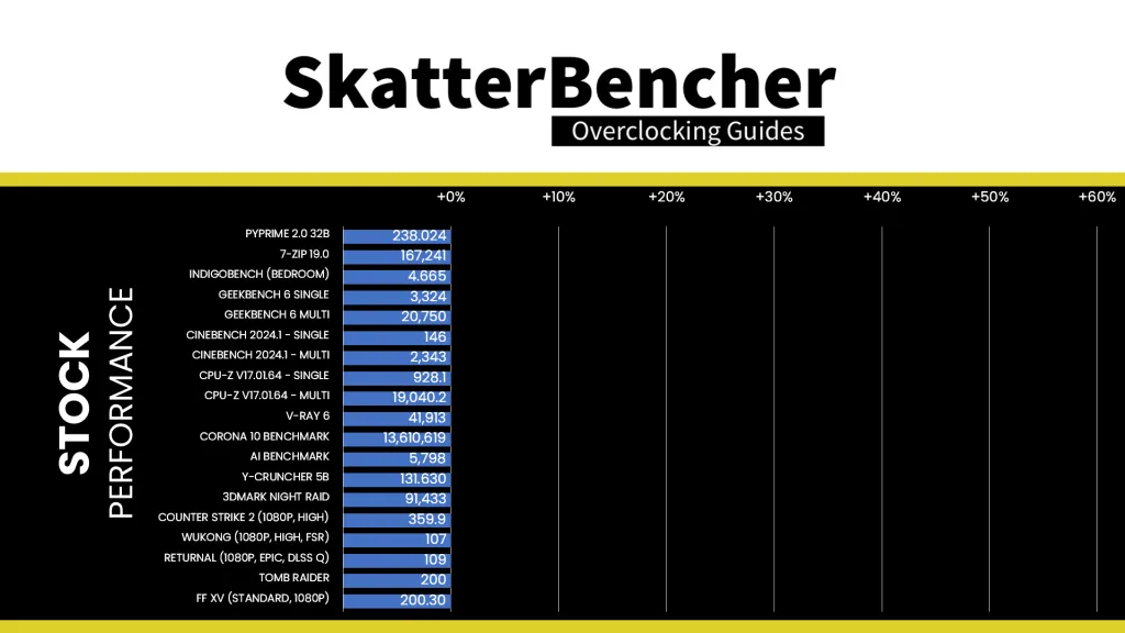
Here is the benchmark performance at stock:
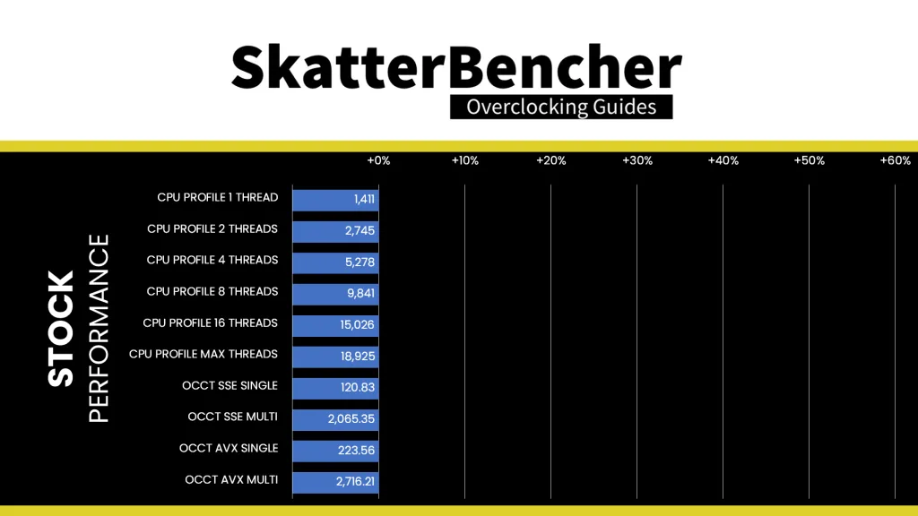
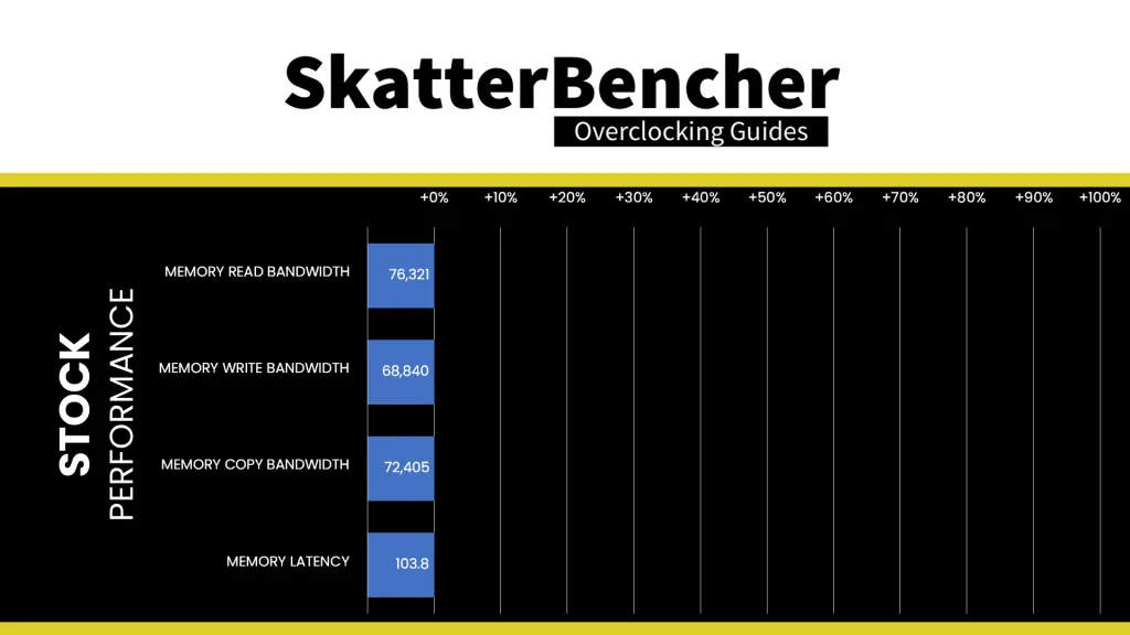
When running the OCCT CPU AVX2 Stability Test, the average CPU P-core effective clock is 5191 MHz with 1.123 volts and the average CPU E-core effective clock is 4427 MHz with 1.033 volts. The average CPU temperature is 85.0 degrees Celsius. The average CPU package power is 247.7 watts.
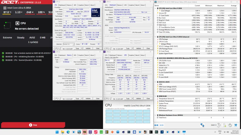
When running the OCCT CPU SSE Stability Test, the average CPU P-core effective clock is 5208 MHz with 1.132 volts and the average CPU E-core effective clock is 4600 MHz with 1.034 volts. The average CPU temperature is 80.0 degrees Celsius. The average CPU package power is 246.2 watts.

Of course, we can increase the performance by unlocking power limits and overclocking the processor. However, before we get going, make sure to locate the CMOS Clear button. Pressing the Clear CMOS button will reset all your BIOS settings to default, which is helpful if you want to start your BIOS configuration from scratch.
OC Strategy #1: ASUS Advanced OC Profile + ASUS MCE + Intel XMP
In our first overclocking strategy, we take advantage of the ASUS Advanced OC Profile, enable MultiCore Enhancement, and rely on Intel Extreme Profile technology.
ASUS Advanced OC Profile
As I mentioned earlier, Intel has clarified the rules of engagement by defining what constitutes default settings. In doing so, it created stricter rules for default BIOS settings but also opened up new avenues for innovation. One such innovation is the ASUS Advanced OC Profile.
In essence, the ASUS Advanced OC Profile set up the BIOS so it’s ready for overclocking. Not only does it reconfigure some of the parameters included in the definition of Intel’s Default Profiles, but it also configures a number of other settings related to power-saving, performance limiters, and so on.
By modifying some parameters, it’s possible to improve the system performance. Most importantly for our guide, however, you’re required to switch to the Advanced OC Profile for any kind of overclocking.
Intel Turbo Boost 2.0 Power Limits
Intel Turbo Boost 2.0 Technology allows the processor cores to run faster than the base operating frequency if the processor is operating below rated power, temperature, and current specification limits. The ultimate advantage is opportunistic performance improvements in both multi-threaded and single-threaded workloads.
The turbo boost algorithm works according to an EWMA formula. This stands for Exponentially Weighted Moving Average. There are three main parameters to consider: PL1, PL2, and Tau.
- Power Limit 1, or PL1, is the threshold that the average power will not exceed. Historically, this has always been set equal to Intel’s advertised TDP. Very importantly, PL1 should not be set higher than the thermal solution cooling limits.
- Power Limit 2, or PL2, is the maximum power the processor is allowed to use for a limited amount of time.
- Tau is a weighing constant used in the algorithm to calculate the moving average power consumption. Tau, in seconds, is the time window for calculating the average power consumption. If the average power consumed is higher than PL1 the CPU will reduce the CPU frequency.
Turbo Boost 2.0 Technology has evolved over the past years to incorporate a lot of power, thermal, and electrical performance limiters, including PL3, PL4, IccMax, TCC_Offset, VR_TDC, RATL, Pmax, and many more.
An easy ASUS MultiCore Enhancement option on ASUS motherboards allows you to unleash the Turbo Boost power limits. Set the option to Enabled – Remove All Limits and enjoy maximum performance. Enabling ASUS MultiCore Enhancement adjusts the following parameters:
| Parameter | Baseline | Performance | Extreme | ASUS MCE |
| ICCMax | 287 A | 347 A | 400 A | 0 |
| ICCMax_App | 210 A | 245 A | N/A | 0 |
| Power Limit 1 (PL1) | 125 W | 250 W | 250 W | 4095 |
| Power Limit 2 (PL2) | 177 W | 250 W | 295 W | 4095 |
| Power Limit 4 (PL4) | 329 W | 425 W | 490 W | 0 |
Intel Extreme Memory Profile 3.0
Intel Extreme Memory Profile 3.0 is the new XMP standard for DDR5 memory and is the successor to XMP 2.0 for DDR4 memory. It was introduced together with the Alder Lake processors in 2021. It is largely based on the XMP 2.0 standard but has additional functionality.
The XMP 3.0 standard is designed with six sections. One global section describes the generic data that is used across all profiles. The other five sections are designed for five profiles respectively.
- Profile 1 is meant for the performance profile (this is the standard XMP as we know it)
- Profile 2 is designed for the extreme settings (this could be a higher frequency at higher voltage)
- Profile 3 is designed for the fastest settings (this could be tighter timings at higher voltage)
- Profiles 4 and 5 are rewritable and meant for user custom settings
Each profile has a wide range of configurable fields related to voltage, frequency, and memory timings, including:
- Voltage: Module VPP, VDD, VDDQ, Memory Controller Voltage
- Primary Timings: tCL, tRCD, tRP, tRAS, Command Rate
- Secondary Timings: tRC, tWR, tRFC1, tRFC2, tRFCsb
- Miscellaneous: Dynamic Memory Boost support, Real-Time Memory Frequency OC support, Vendor ID
XMP allows memory vendors such as G.SKILL to program higher performance settings onto the memory sticks. If the motherboard supports XMP, you can enable higher performance with a single BIOS setting. So, it saves you lots of manual configuration.
It’s the first time I’m using this particular DDR5-8400 memory kit for an overclocking guide. Unfortunately, I can’t run the XMP out of the box and have to reduce the memory frequency to DDR5-8000 while retaining all other settings of the XMP profile.
BIOS Settings & Benchmark Results
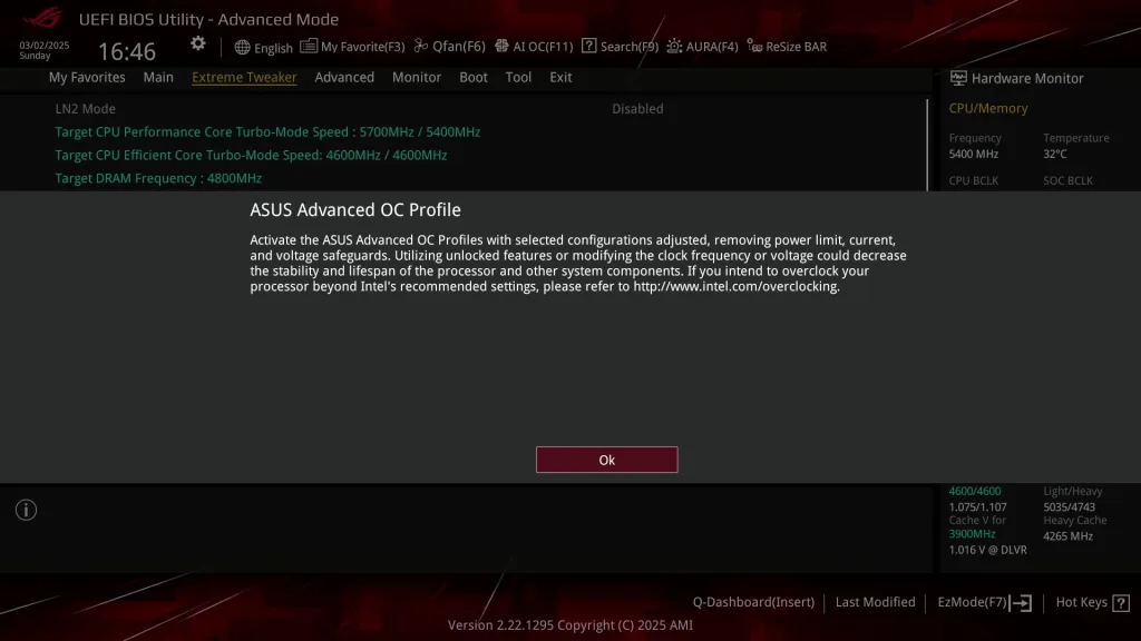
Upon entering the BIOS
- Go to the Extreme Tweaker menu
- Set Performance Preferences to ASUS Advanced OC Profile
- Set Ai Overclock Tuner to XMP I
- Set ASUS MultiCore Enhancement to Enabled – Remove All Limits
- Set DRAM Frequency to DDR5-8000
Then save and exit the BIOS.
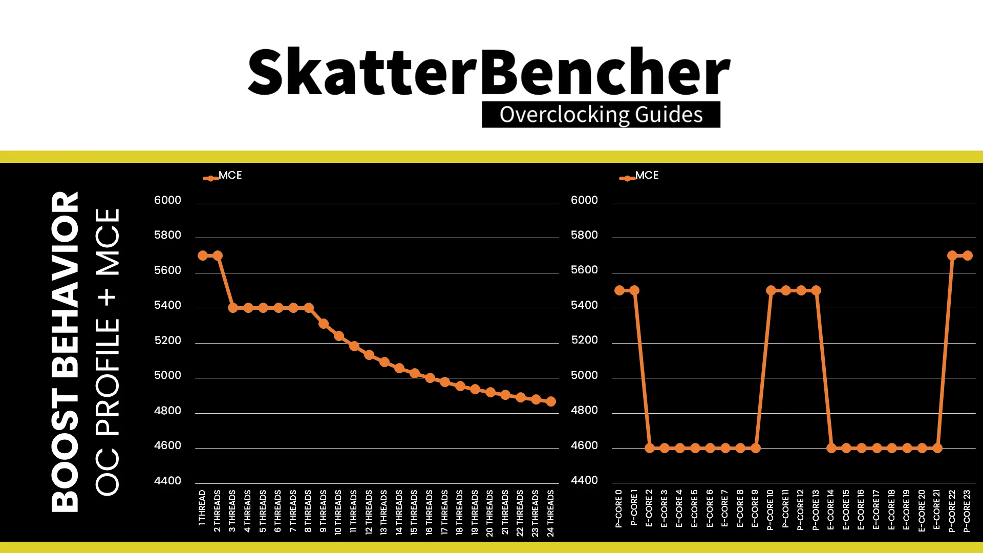
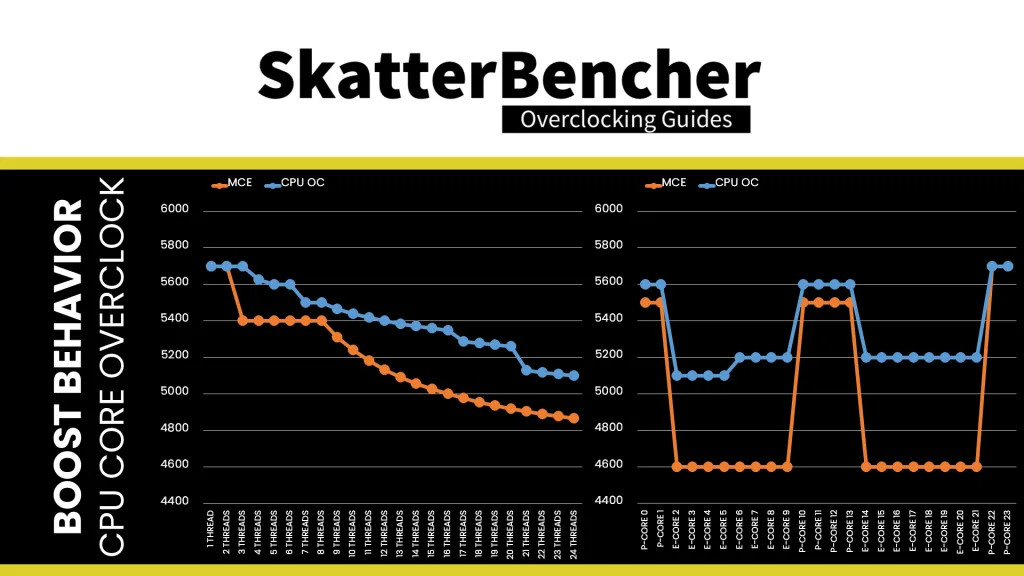
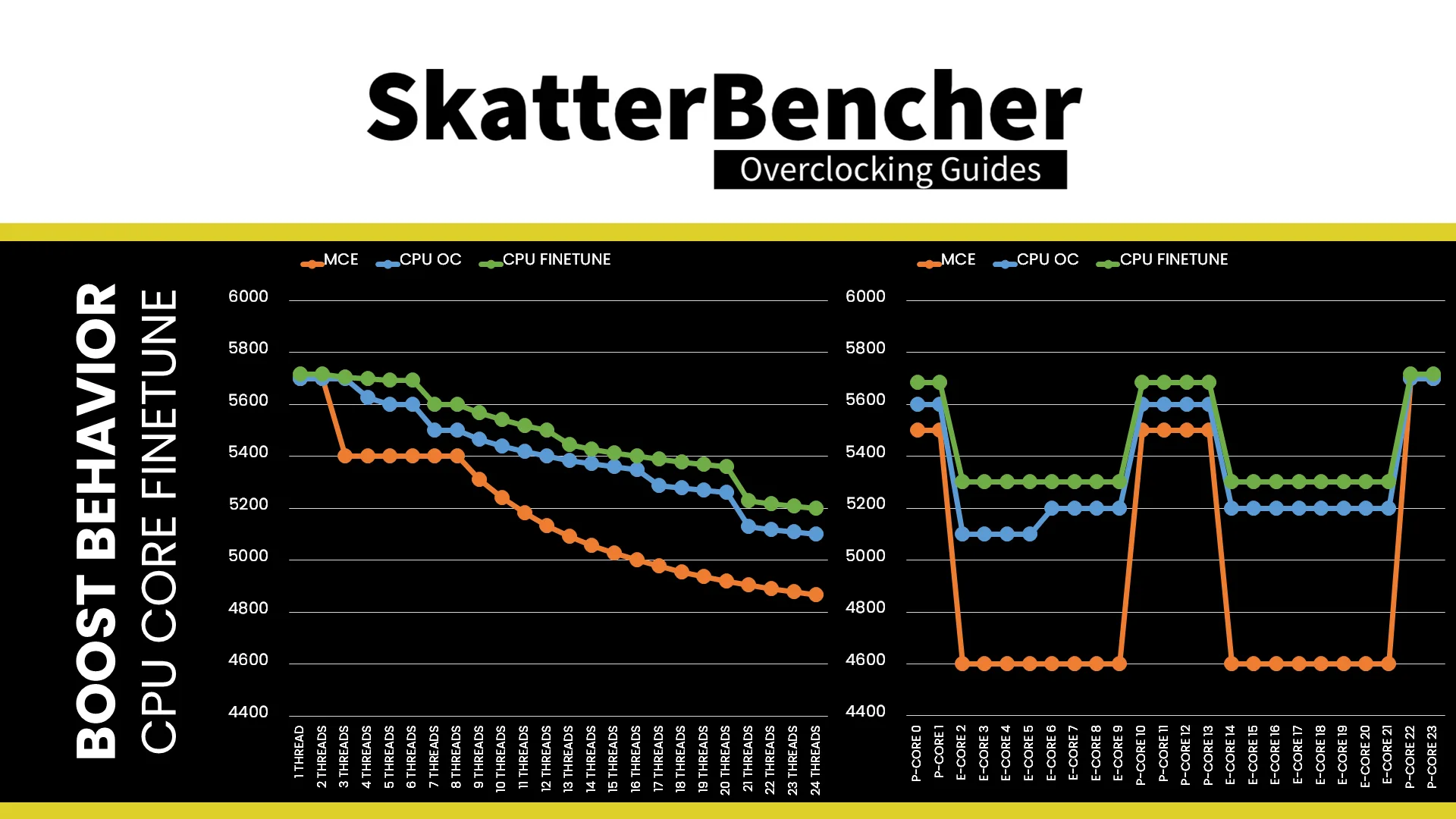
The CPU boost frequency with 1 active P-core is 5700 MHZ. The average boost frequency gradually trails off to 5400 MHz when all P-cores are active and to 4867 MHz when all P- and E-cores are active. The two favored P-cores can boost to 5.7 GHz, the six other non-favored cores can boost to 5.4 GHz, and every E-core can boost to 4.6 GHz in single-threaded workloads.
We re-ran the benchmarks and checked the performance increase compared to the default operation.
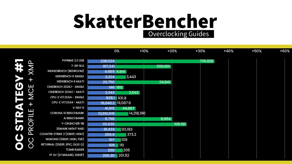
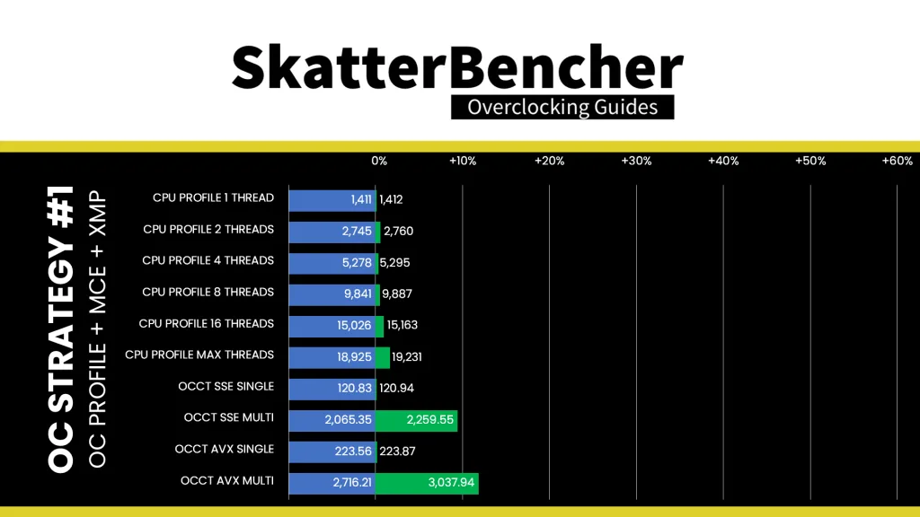
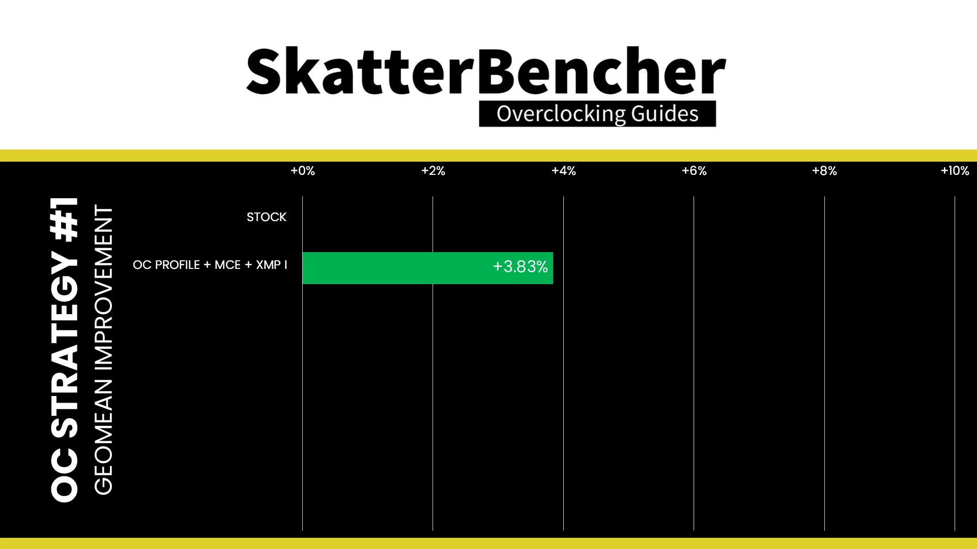
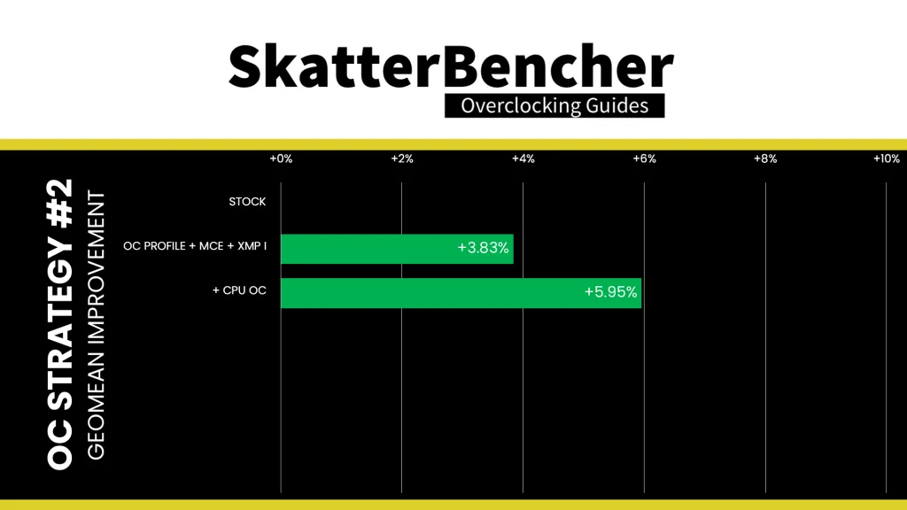
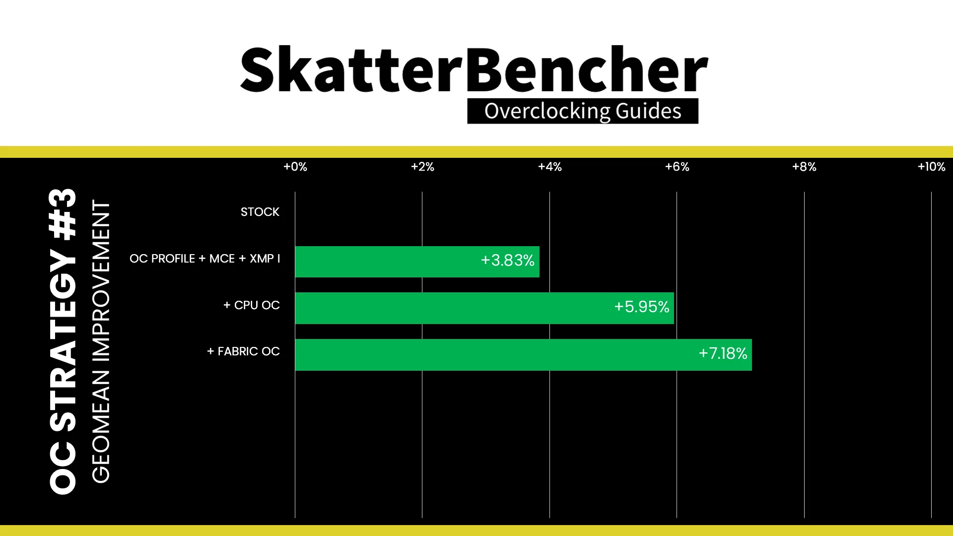
The Core Ultra 9 285K is the most powerful of all Arrow Lake K-SKU processors and thus limited by power and memory performance. By unlocking the power limits and enabling XMP, we get a nice uplift across the board, especially in multi-threaded, memory-hungry applications like Y-Cruncher and AI Benchmark. The Geomean performance improvement is +3.83%, and we get a maximum improvement of +34.99% in PyPrime.
When running the OCCT CPU AVX2 Stability Test, the average CPU P-core effective clock is 5297 MHz with 1.157 volts and the average CPU E-core effective clock is 4601 MHz with 1.047 volts. The average CPU temperature is 95.0 degrees Celsius. The average CPU package power is 297.9 watts.

When running the OCCT CPU SSE Stability Test, the average CPU P-core effective clock is 5293 MHz with 1.148 volts and the average CPU E-core effective clock is 4586 MHz with 1.046 volts. The average CPU temperature is 85.0 degrees Celsius. The average CPU package power is 275.4 watts.

OC Strategy #2: CPU Overclock
In our second overclocking strategy, we finally overclock the CPU cores. For this we rely on two foundational overclocking technologies: Turbo Ratio Limit and Adaptive Voltage mode.
Turbo Ratio Limit
Intel Turbo Ratio Limit is a technology that regulates the Turbo Boost frequency of an Intel processor based on the number of active cores.
Intel processors usually have two types of CPU core frequencies specified: the base frequency and the Turbo Boost frequency. The base frequency is also known as the “Maximum Non-Turbo Ratio” whereas the turbo frequency is usually referred to as the Turbo Ratio Limit.
The Turbo Ratio Limit is called a limit because it restricts the operating frequency rather than targets a frequency. Processors like the Core Ultra 9 285K have an upper core frequency ratio of 120X. Without the ratio limit, the CPU would boost its frequency all the way to the maximum frequency. However, the Turbo Ratio Limit specifies an upper ceiling to the boost frequency.
The tool is pretty flexible and can be programmed for various scenarios. The ratio limits are defined in the processor’s Machine Specific Registers (MSRs) by two parameters:
- The Turbo Ratio Limit
- The number of active cores
For CPUs like the Core Ultra 9 285K, which have no more than 8 P-cores, these registers are configured from 1-active P-core to 8-active P-cores. However, on platforms with core counts beyond eight cores, we can configure each register by target Turbo Boost Ratio and the number of active cores.
Furthermore, on hybrid designs like Alder Lake, Raptor Lake, or Arrow Lake, which all feature a combination of P-cores and E-cores, the Turbo Ratio Limit configuration is specified by core type. In other words: the applied ratio limit for the P-cores is independent from the limit of the E-cores.
For example, on the Core Ultra 9 285K the Turbo Ratio Limit specifies 57X when up to 2 P-cores are active, 54X when 3 or more P-cores are active, and 46X for any amount of active E-cores. In theory, if 2 P-cores and all E-cores are active, the P-cores would operate at 57X even though more than 2 cores in total are active.
Note that configuring the turbo ratio is not the same as configuring each core individually. When using turbo ratio limit, we determine an overclock according to CPU usage. For example, if a workload uses four cores, the CPU determines which cores should execute this workload and applies our set frequency to those cores.
The Turbo Ratio Limit configuration also has a couple of rules that must be followed:
- Each register must be defined by a target ratio and a number of active cores.
- The minimum allowed ratio limit is the maximum non-turbo ratio.
- The maximum allowed ratio limit is defined per architecture.
- On modern CPUs that’s 85X or 120X using extended ratio mode
- The ratio limit of a register must be equal to or lower than the ratio defined for the previous register .
- E.g. we cannot define 60X for up to 1 active core and 62X for up to 4 active cores.
- The core count of a register must be equal to or lower than the ratio defined for the previous register.
- E.g. we cannot define register 1 to define the ratio for up to 5 active cores and register 2 to define the ratio for up to 2 active cores
- The last register must always define the ratio limit for the highest available active cores of the processor SKU.
Per Core Ratio Limit
Per Core Ratio Limit allows you to set a maximum CPU Ratio for every P-core and E-core cluster individually. It is an extension of the Intel Turbo Boost Max 3.0 technology introduced in 2016. It acts independently from the Turbo Ratio Limit, meaning that when you set a Per Core Ratio Limit, the core ratio will be restricted even if the Turbo Ratio Limit allows for a higher boost frequency.

The Per Core Ratio Limit plays an important role in the Arrow Lake overclocking process. It’s not only the ratio used in the V/F point configuration but also the ratio referenced by many other ratio tuning technologies.
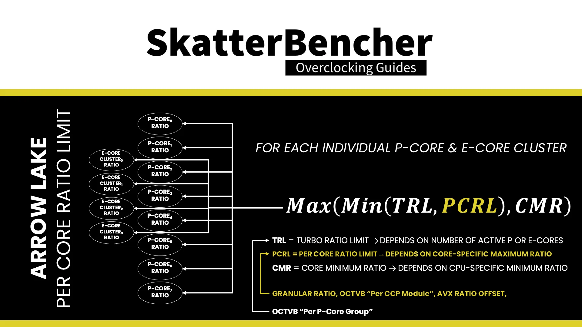
In our case, we’ll use it to restrict the cores with less overclocking headroom to boost as high as the cores with great headroom.
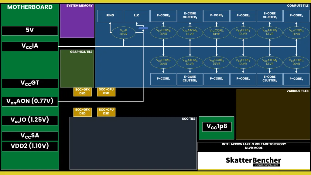
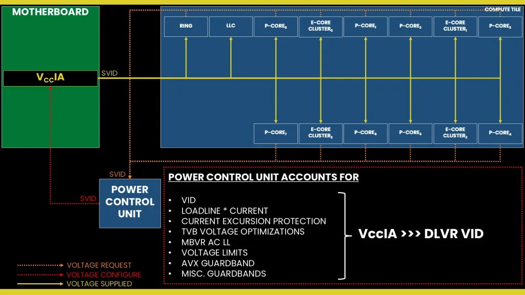
Arrow Lake Voltage Topology
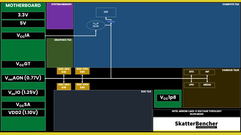
The voltage regulation for the P-cores is more complex than prior generations of Intel Core processors due to the introduction of the Digital Linear Voltage Regulator (DLVR). The DLVRs enable much lower voltage levels for the cores and ring but still rely on a dynamic external motherboard voltage regulator as the input voltage source.
VccIA, VccCORE, & VccATOM
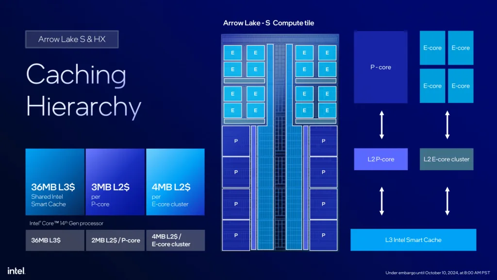
The external VccIA motherboard voltage regulator (MBVR) provides the input voltage for the individual P-core, E-core clusters, Ring, last-level cache (LLC), and E-core L2 cache. Each P-core, E-core cluster, and Ring has an individual Digital Linear Voltage Regulator (DLVR) between the VccIA rail and the IP blocks. That means each of the blocks can operate at its own voltage.
- VccCOREn is the DLVR powering an individual P-core.
- VccR is the DLVR powering the Ring and Last-Level Cache.
- VccATOMn is the DLVR powering an individual E-core cluster, which consists of four E-cores, and its L2 cache.

The DLVRs can also be bypassed. In that case, the IP blocks are running in so-called Power Gate (PG) mode. We’ll cover that later in the video.
V/F Curves
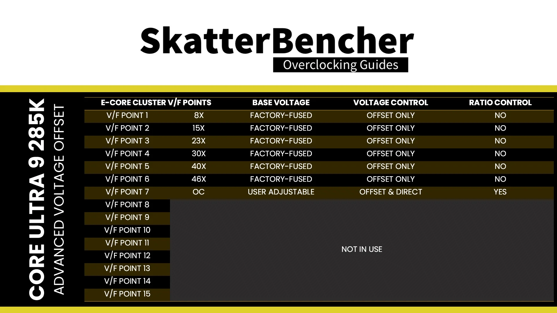
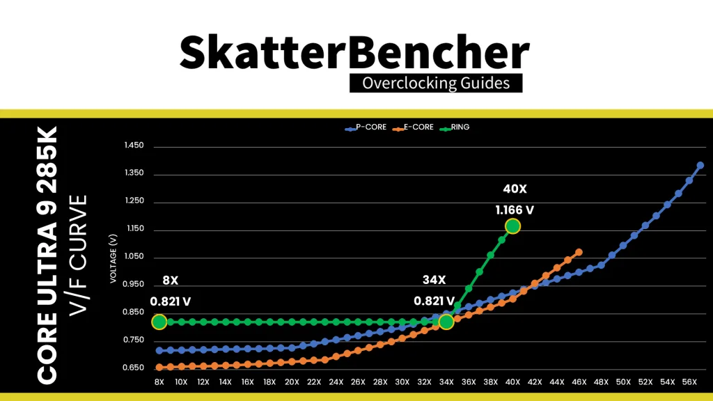
Each Core Ultra 9 285K P-core and E-core cluster also has its own V/F curve which is defined by nine (9) V/F points for the P-cores and seven (7) V/F points for the E-core clusters. The first eight (8) V/F points are factory-fused, and the last point is mapped to the “OC Ratio.”
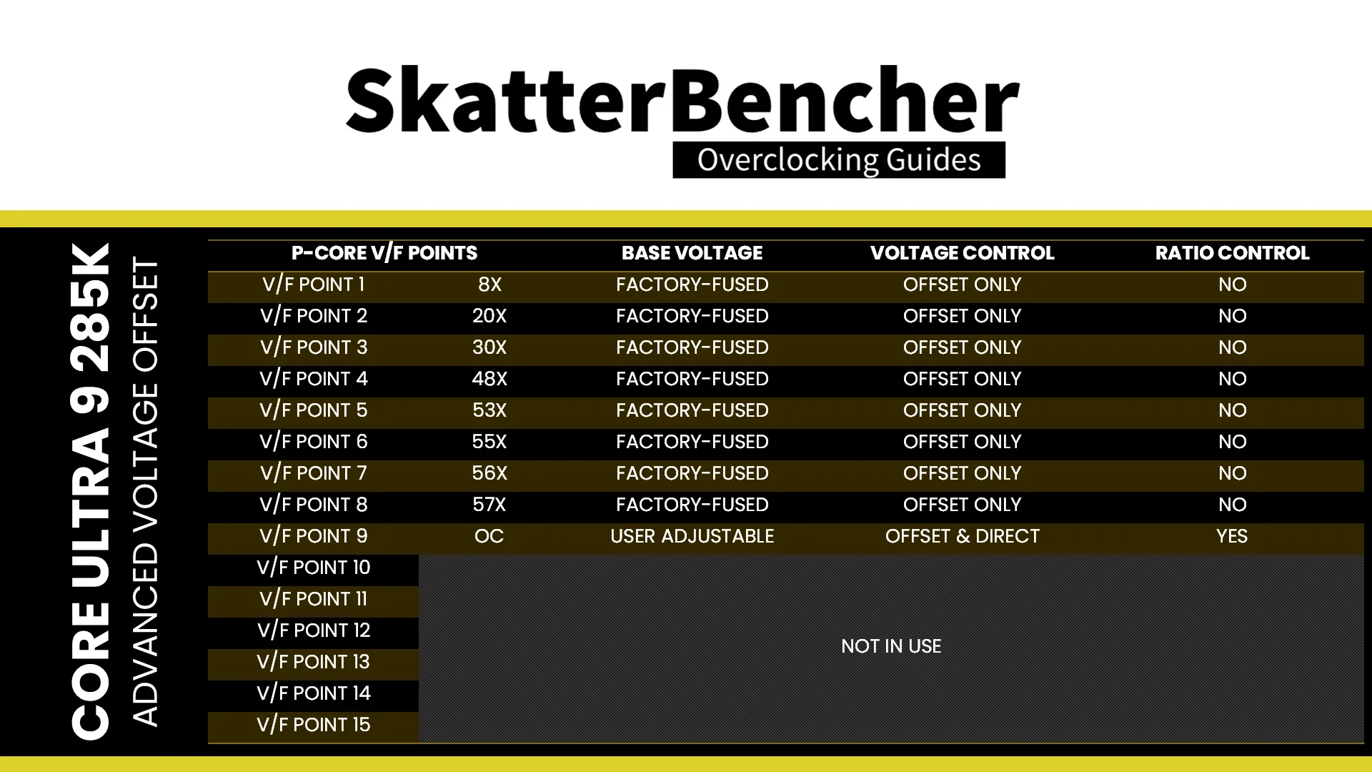
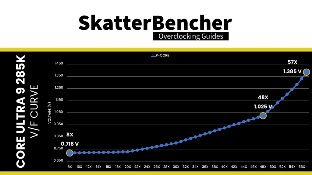
Here is the aggregate P-core V/F curve for my specific Core Ultra 9 285K. The voltage is about 718 mV at 800 MHz, then increases to 1.025V for VF Point 4 at 4.8 GHz, and ultimately ends at 1.385V for V/F Point 9 at 5.7 GHz. Each P-core has a different fused voltage for V/F Point 6 which ranges from 1.266V for Core 1 to 1.324V for Core 4.
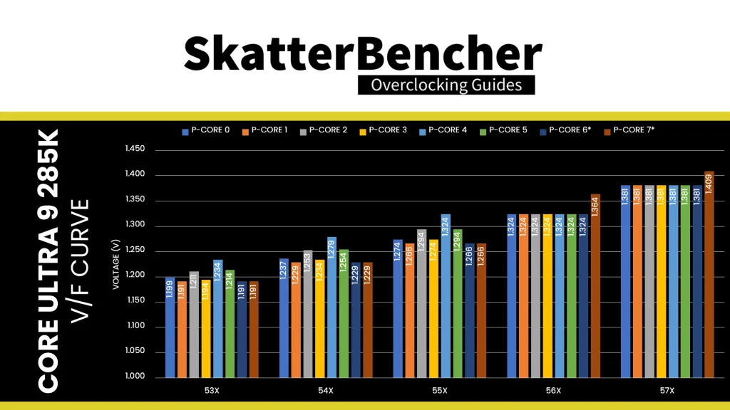
We need to make a special note about V/F Points 7 and 8 for the non-favored P-cores. While it may seem from the graph they have independent values, that’s not entirely correct. And it’s quite complicated.
- On older dCode, the non-favored cores have pre-defined values for V/F Points 7 & 8, which is determined by the highest value of the respective favored core V/F Points.
- On newer dCode, the favored cores don’t have pre-defined values for V/F Points 7 & 8, meaning their V/F curve ends at V/F Point 7.
For this particular system, we’re using the older dCode which explains why the non-favored cores have pre-defined voltages for V/F Points 8 and 9.
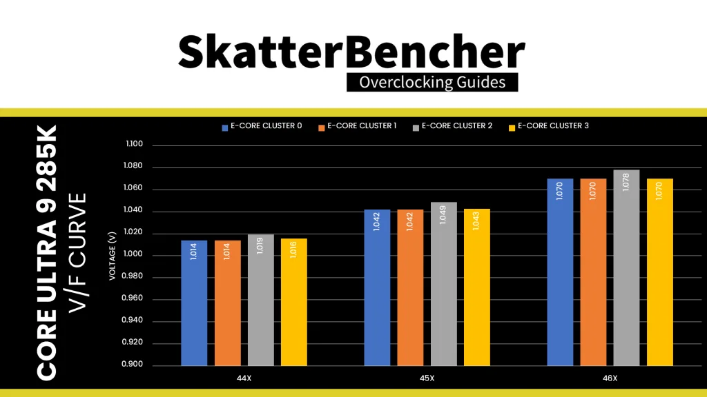
Here is the aggregate E-core V/F curve for my specific Core Ultra 9 285K. The voltage is about 659 mV at 800 MHz, then increases to 762 mV for VF Point 4 at 3.0 GHz, and ultimately ends at 1.072V for V/F Point 6 at 4.6 GHz. Each E-core has a different fused voltage for V/F Point 6 which ranges from 1.070V for E-core clusters 0, 1, and 3 to 1.078V for E-core cluster 2.

Adaptive Voltage Mode
Based on the VF curve, the CPU cores request an operating voltage using the SVID protocol from the CPU Power Control Unit (PCU). The PCU in turn configures the VccIA voltage rail and the individual DLVRs. There are two ways to configure the DLVR voltage:
- Adaptive mode is the standard mode of operation, which relies on the factory-fused voltage-frequency curves we discussed before.
- Override mode specifies a single static voltage across all ratios. It is mainly used for extreme overclocking where stability at high frequencies is the only consideration.
We can configure override and adaptive modes directly in the PCU by specifying a target voltage and a voltage offset for each mode.
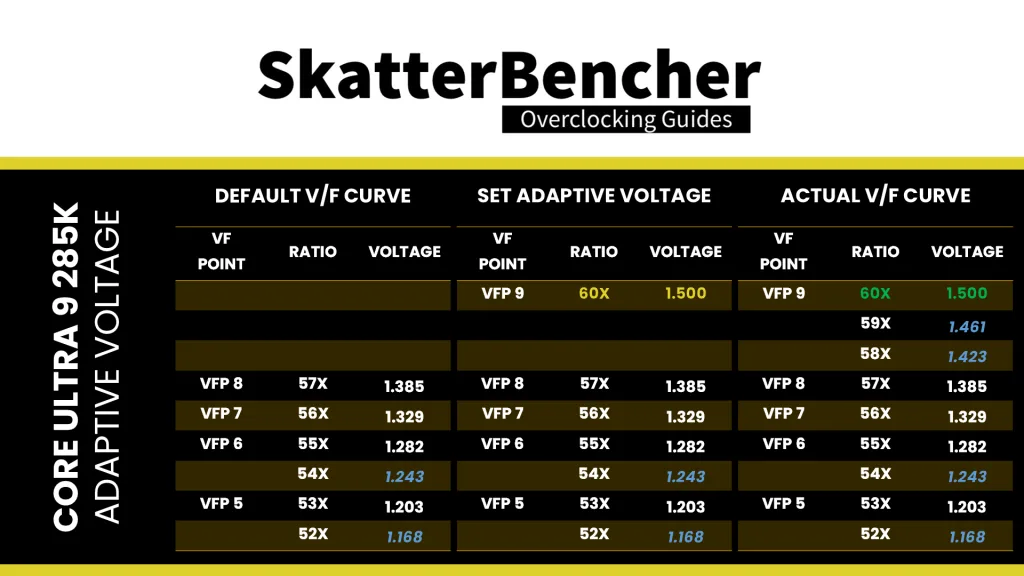
In adaptive mode, the target voltage is mapped to a core’s “OC Ratio.” Each P-core and E-core cluster has its own “OC Ratio” which is defined by the Per Core Ratio Limit. This also matches V/F Point 9 for the P-cores and V/F Point 7 for the E-cores. You can configure the adaptive voltage and OC Ratio to any value; however, multiple rules enforce what ratio and voltage are actually set.
Rule #1: the voltage set for a given VF Point n must be higher than or equal to the voltage set for VF Point n-1.
That means the voltage for the OC Ratio, matching V/F Point 9, must be higher than or equal to the voltage for VF Point 8.
For example, let’s say you set the P-core Per Core Ratio Limit to 59X and the adaptive voltage to 1.1V. In that case, VF Point 9 will be programmed to 59X at 1.1V. However, the actual frequency will be 5.9 GHz with 1.385V, as that’s the voltage for VF Point 8.

Even if you set the voltage lower in BIOS, the PCU will override your configuration if it doesn’t follow the rules.
Rule #2: for ratios between the OC Ratio and the next highest factory-fused V/f point, the voltage is interpolated between the set adaptive voltage and the factory-fused voltage.
Let’s say we configure the P-core V/F OC Point to 60X and 1.50V. The target voltage for each P-core ratio between 57X and 60X is now interpolated between the P-core’s factory-fused voltage for 57X and the set adaptive voltage for 60X.
There are several ways to configure the adaptive voltage, including setting it for each P-core and E-core cluster individually. In this OC Strategy, we set a single, global adaptive voltage that’s used for every core’s “OC Ratio.”
Thermal Velocity Boost
Thermal Velocity Boost is an Intel technology that exploits the fact that CPUs need less voltage to run a specific frequency when the operating temperature is lower. On some CPUs like the Core Ultra 9 285K, Intel leverages this to decrease the Turbo Ratio when the CPU is operating above a certain temperature.
For the Core Ultra 9 285K, the default Thermal Velocity Boost configuration decreases the Turbo Ratio by 1 bin when 2 or more P-cores are active and running above 70 degrees Celsius. For example, the default P-core Turbo Ratio when all 8 cores are active is 54X. However, it’ll downclock to 53X when the operating temperature exceeds 70 degrees Celsius. We can see this behavior in the OCCT results from the previous OC Strategy where, despite temperature and power headroom, the P-core frequency is limited to 5.3 GHz.
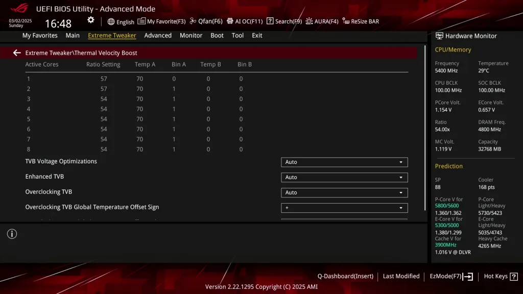
We can easily disable this behavior through OCTVB configuration by forcing the down-bin to 0 regardless of the TVB configuration.
Thermal Velocity Boost Voltage Optimizations
Thermal Velocity Boost is an Intel technology that exploits the fact that CPUs need less voltage to run a specific frequency when the operating temperature is lower. When this technology is enabled, the CPU automatically adjusts the operating voltage according to the operating temperature.
For example, for my Arrow Lake launch content, I collected data for the Core Ultra 9 285K to illustrate this behavior. As you can see from the data, with the P-core at 5.4 GHz, the operating voltage is 1.237V when the temperature is below 50 degrees Celsius. However, it increases to nearly 1.3V when the temperature approaches 100 degrees Celsius. A regression analysis tells us that the operating voltage changes 1.1 mV for every change in degree Celsius.
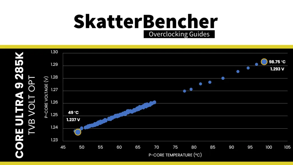
If you want manual control over the operating voltage to ensure stability, like when you’re trying to overclock, it’s prudent (but not mandatory) to disable this function.
Arrow Lake P-core and E-core Tuning Process
The manual tuning process for Arrow Lake can be difficult because there’s a wide range of workload and operating scenarios to test. Furthermore, as you’ll get to see in throughout this guide, the Core Ultra 9 285K CPU cores don’t have that much overclocking headroom and don’t scale particularly well with voltage.
We can break down the basic tuning process into three steps: choosing the voltage, checking for per core stability, then lastly adjusting for all-core stability.
Choosing the Voltage
Usually, I determine an appropriate starting point for the adaptive voltage by first considering the current maximum voltage and then adding 50 to 200mV.
However, that’s not ideal for the Core Ultra 9 285K P-cores because the default maximum voltage is already 1.4V and there’s limited to no scaling with voltage. So instead, I force the P-cores to follow the V/F curve and see how much headroom there is with the default voltage. Side-note: to avoid the motherboard auto-rules configuring the voltage for you, you can set the Adaptive Voltage to 0.6V.
For the E-cores, the default maximum voltage is pretty low at 1.070V, so I increase the adaptive voltage to 1.25V.
Note that we want full control over the effective voltage, so make sure to disable any technologies that might adjust the operating voltage such as TVB Voltage Optimizations or Advanced Voltage Offset.
1T Stability
After you’ve set your target adaptive voltage, you can find the maximum stable frequency for each P-core and E-core cluster at that voltage. The easiest way to do that is by setting the Turbo Ratio Limit to, for example, 60X, and then setting the Per Core Ratio Limit to the frequency you want to test. For example, a starting point of 57X for the P-cores and 48X for the E-cores.
Now, you can run a stress of choice. I typically rely on the OCCT CPU Stress Test which has a built-in core cycling function. But you can also run a custom application like Core Cycler or pick a different stress test. You can start with a 30 second quick test first to quickly find the upper limit, then longer test times to confirm stability.
Strangely enough, for the Core Ultra 9 285K, I found AI Benchmark to be the most difficult benchmark to pass with a high Per P-core Core Ratio Limit despite it being a multi-threaded benchmark. I attribute this to the benchmark being a highly transient memory-dependent AVX workload. It seems that the combination of a demanding workload and dynamic power profile causes is the main constraint for stabilizing the high frequencies.
The E-cores behave much more consistently, and I don’t see the same instabilities in AI Benchmark.
nT Stability
Finally, we need to check if the CPU is also stable in non-single-thread workloads. The easiest way to do this is by running your worst-case all-core workload which, in my case, is always 30 minutes of OCCT CPU AVX2 Stability Test.
You’ll typically find that the CPU cannot run all-core at the same frequency as it can run single-threaded workloads. If that’s the case, simply lower the Turbo Ratio Limit for all-core workloads until it’s stable.
In addition to the OCCT CPU AVX2 Stability Test, I generally also include three other workloads during all-core testing: Y-Cruncher, Cinebench R23, and AI Benchmark. While these three test are no replacement for the worst-case stress test, they highlight different kinds of instabilities – usually related to transient loads.
Final Result
Sticking with the factory-fused V/F curve for the P-cores, I could increase the non-favored P-cores to 5.6 GHZ. The favored P-cores have no overclocking headroom. I could also increase the all-P-core Turbo Ratio by 100 MHz to 5.5 GHz.
With 1.250V adaptive voltage for the E-cores, I could increase three E-core clusters by 600 MHz to 5.2 GHz while the other cluster could only hit 5.1 GHz. In all core workloads, the maximum stable E-core frequency is 4.9 GHz.
BIOS Settings & Benchmark Results
Upon entering the BIOS
- Go to the Extreme Tweaker menu
- Set Performance Preferences to ASUS Advanced OC Profile
- Set Ai Overclock Tuner to XMP I
- Set ASUS MultiCore Enhancement to Enabled – Remove All Limits
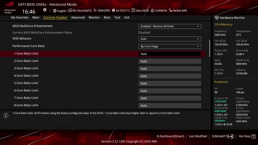
- Set Performance Core Ratio to By Core Usage
- Set 1-Core to 4-Core Ratio Limit to 57
- Set 5-Core and 6-Core Ratio Limit to 56
- Set 7-Core and 8-Core Ratio Limit to 55
- Enter the Specific Performance Core submenu
- Set Performance Core0 to Core5 Specific Ratio Limit to 56
- Set Performance Core6 and Core7 Specific Ratio Limit to 57
- Leave the Specific Performance Core submenu
- Set Efficient Core Ratio to By Core Usage
- Enter the By E-Core Usage submenu
- Set Efficient Turbo Ratio Limit 1 to 52
- Set Efficient Turbo Ratio Cores 1 to 8
- Set Efficient Turbo Ratio Limit 2 to 51
- Set Efficient Turbo Ratio Cores 2 to 12
- Set Efficient Turbo Ratio Limit 3 to 49
- Set Efficient Turbo Ratio Cores 3 to 16
- Leave the By E-Core Usage submenu
- Enter the Specific Efficient Core submenu
- Set Efficient Core Group0 Specific Ratio Limit to 51
- Set Efficient Core Group1 to Group3 Specific Ratio Limit to 52
- Leave the Specific Efficient Core submenu
- Set DRAM Frequency to DDR5-8000
- Enter the Thermal Velocity Boost submenu
- Set TVB Voltage Optimizations to Disabled
- Set Overclocking TVB to Enabled
- Set OC TVB Configuration Limit to Per P-core Group
- Set OC TVB Ratio Item Mode to All Core Mode
- Set All core to Enabled
- Set Negative Ratio Offset A to 0
- Set Negative Ratio Offset B to 0
- Leave the Thermal Velocity Boost submenu
- Enter the Performance Core V/F Point Offset submenu
- Set V/F Point Present Mode to All Core Mode
- Set V/F Point Voltage Control Mode to Manual Mode
- Leave the Performance Core V/F Point Offset submenu
- Enter the Efficient Core V/F Point Offset submenu
- Set V/F Point Present Mode to All Core Mode
- Set V/F Point Voltage Control Mode to Manual Mode
- Leave the Efficient Core V/F Point Offset submenu
- Set Performance Core DLVR Voltage to Adaptive Mode
- Set Additional Turbo mode Voltage to 0.600
- Set Efficient Core DLVR Voltage to Adaptive Mode
- Set Additional Turbo mode Voltage to 1.250
Then save and exit the BIOS.
The CPU boost frequency with 1 active P-core is 5700 MHZ. The average boost frequency gradually trails off to 5500 MHz when all P-cores are active and to 5100 MHz when all P- and E-cores are active. In single-threaded applications, two P-cores can boost to 5.7 GHz and six can boost up to 5.6 GHz. Three E-core clusters can boost to 5.2 GHz and one to 5.1 GHz.
We re-ran the benchmarks and checked the performance increase compared to the default operation.
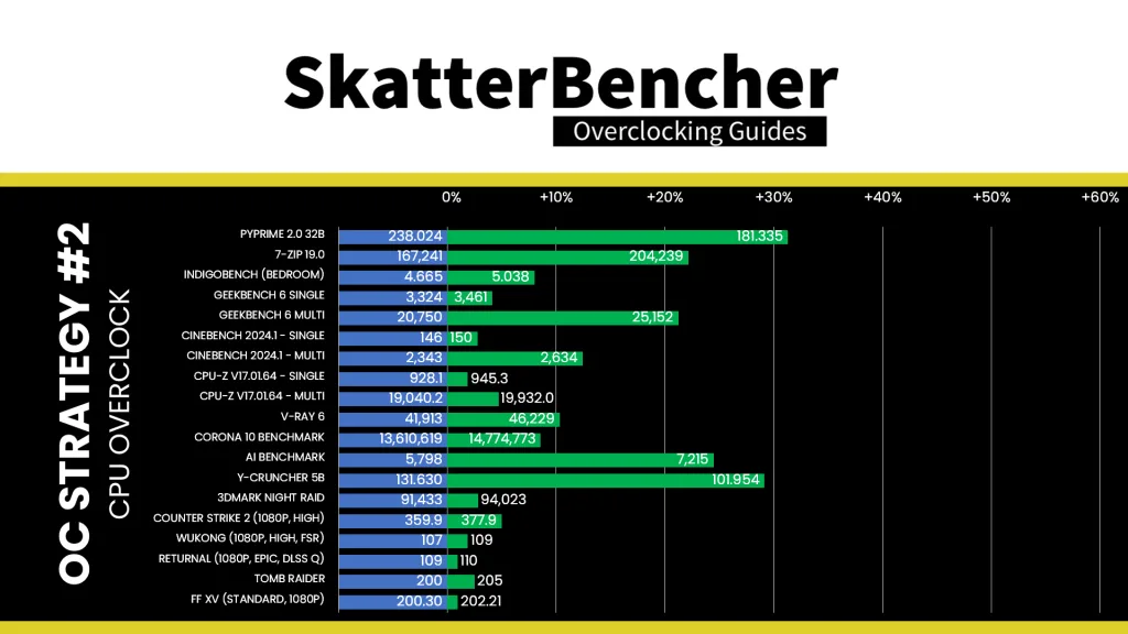
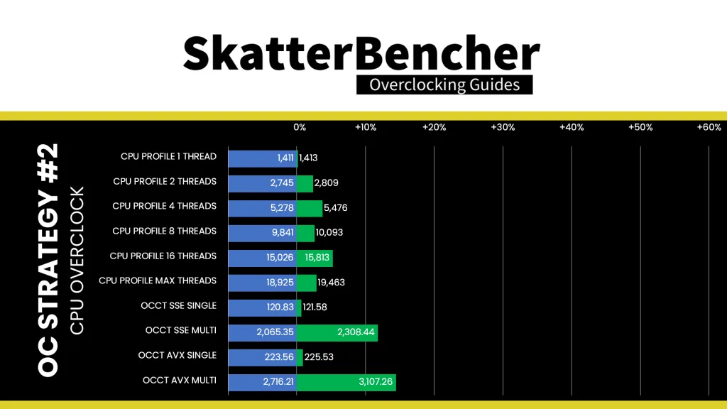
While the P-core overclocking headroom is very limited, we are able to squeeze the E-cores for performance. Overall, however, the frequency increase is not that much and that also translates into a not-so great performance improvement. The Geomean performance improves by another 2.12 percentage points, and we get a maximum improvement of +31.26% in PyPrime.
When running the OCCT CPU AVX2 Stability Test, the average CPU P-core effective clock is 5388 MHz with 1.257 volts and the average CPU E-core effective clock is 4901 MHz with 1.172 volts. The average CPU temperature is 105.0 degrees Celsius. The average CPU package power is 357.0 watts.
When running the OCCT CPU SSE Stability Test, the average CPU P-core effective clock is 5489 MHz with 1.242 volts and the average CPU E-core effective clock is 4834 MHz with 1.172 volts. The average CPU temperature is 105.0 degrees Celsius. The average CPU package power is 369.5 watts.

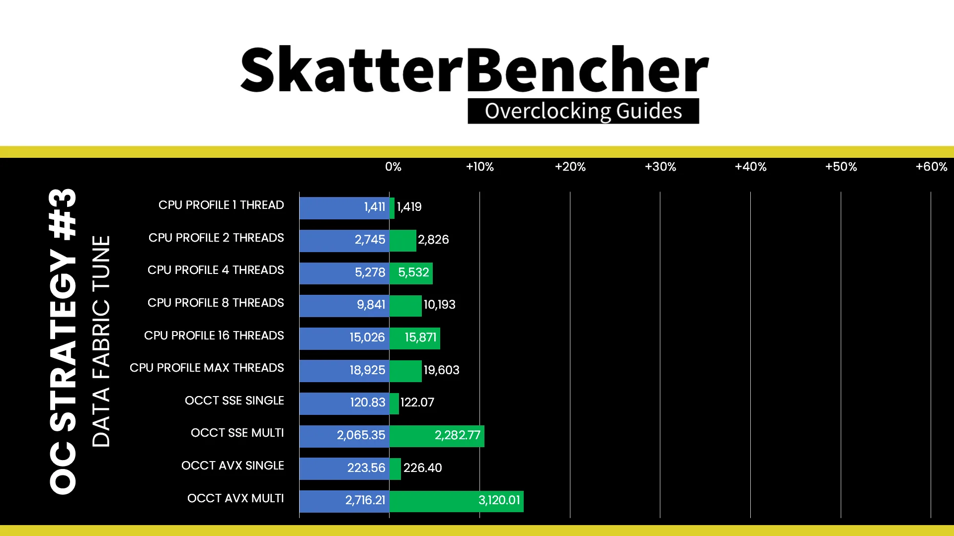
OC Strategy #3: Data Fabric Tuning
In our third overclocking strategy, we delve into tuning the data fabric which consists of the Ring, the NoC in the NGU, and the CPU D2D interface.
Ring
The Ring fabric provides the data fabric interface between the various Compute IP blocks in the Compute Tile, the last-level cache, and the SOC-Compute D2D interface.
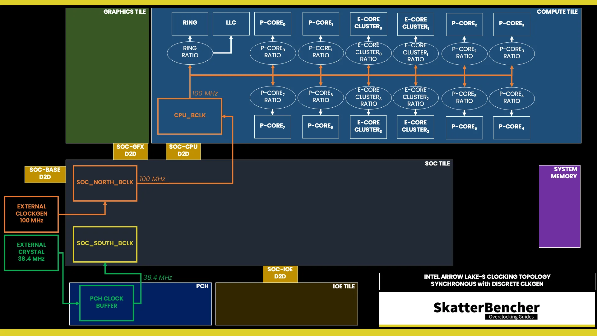
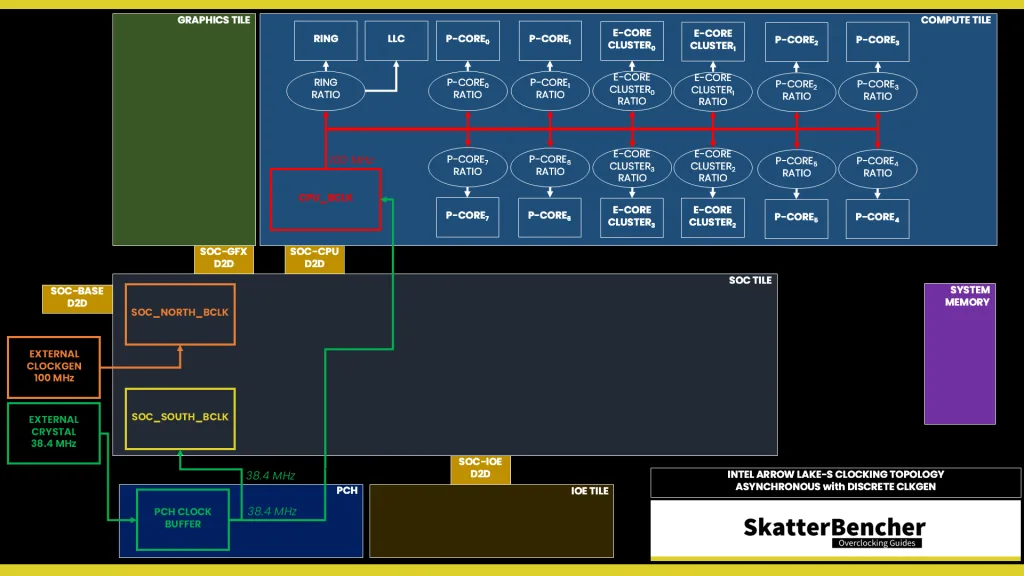
Ring Clocking Topology
The Ring reference clock frequency is generated internally by the CPU PLL. This clock affects all IP blocks in the Compute Tile, including the P-cores, E-cores, and Ring. This PLL can be linked to the SoC PLL when you run in synchronous mode or work independently if you run in asynchronous mode.
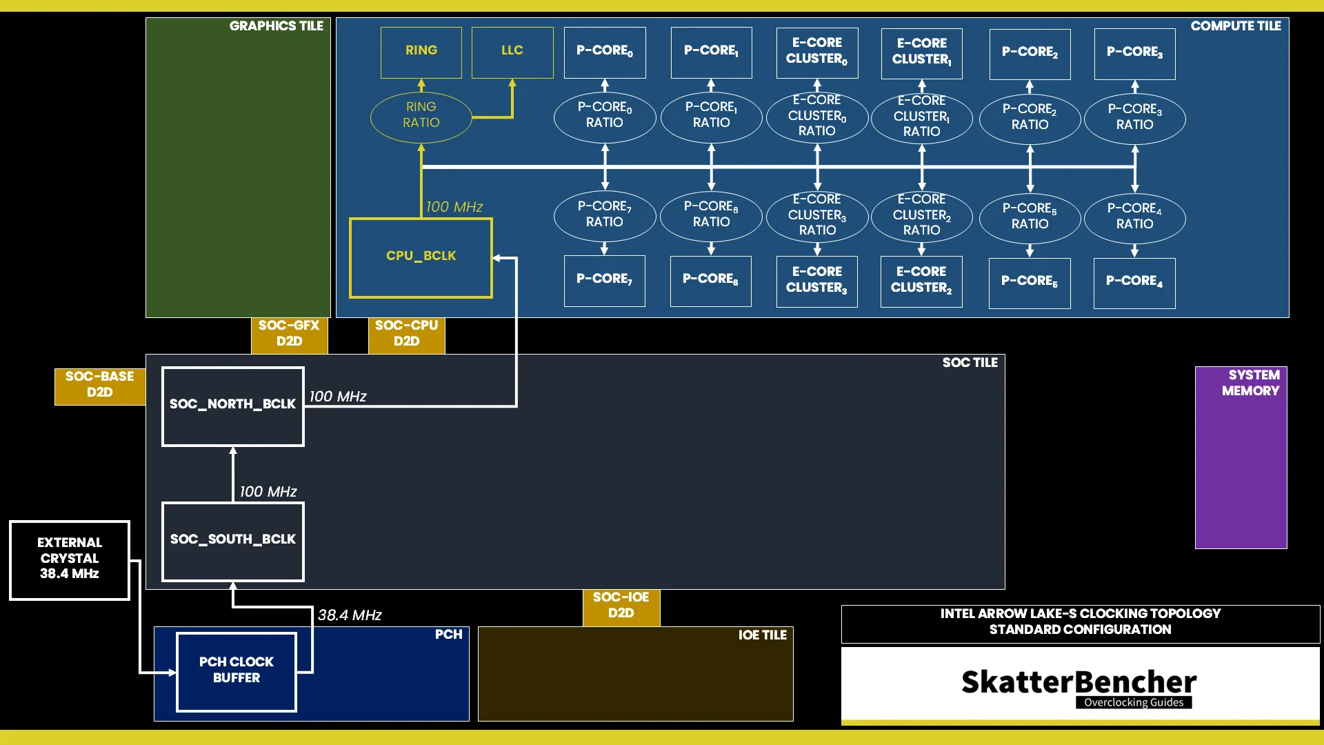
The reference clock is multiplied by the Ring ratio to achieve the final clock frequency. It operates independently from the P-cores and the E-cores. The default ratio is 39X, which yields a 3.9 GHz operating frequency.
Ring Voltage Topology
The voltage regulation for the Ring is more complex than prior generations of Intel Core processors due to the introduction of the DLVR. The DLVR enables much lower voltage levels for the Ring but still relies on a dynamic external motherboard voltage regulator as the input voltage source.
As we discussed earlier in the guide, the external VccIA motherboard voltage regulator (MBVR) provides the input voltage for DLVRs of the individual P-core, E-core clusters, Ring, last-level cache (LLC), and E-core L2 cache.
- VccCOREn is the DLVR powering an individual P-core.
- VccR is the DLVR powering the Ring and Last-Level Cache.
- VccATOMn is the DLVR powering an individual E-core cluster, which consists of four E-cores, and its L2 cache.
The DLVRs can also be bypassed. In that case, the IP blocks are running in so-called Power Gate (PG) mode. We’ll cover that later in the video.
V/F Curve
The Core Ultra 9 285K Ring has its own V/F curve which is defined by up to nine (9) V/F points. The first eight (8) V/F points are factory-fused, and the last point is mapped to the “OC Ratio.” Oddly enough, while the default Ring frequency is 3.9 GHz, the V/F curve is actually defined up to 4.0 GHz!

Here is the Ring V/F curve for my specific Core Ultra 9 285K. The voltage is about 821 mV at 800 MHz all the way up to 3.4 GHz, then increases nearly linearly to 1.116V for VF Point 8 at 4.0 GHz.
Adaptive Voltage Mode
Similar to the P-cores and E-cores, the Ring requests an operating voltage using the SVID protocol from the CPU Power Control Unit (PCU) based on its VF curve. The PCU in turn configures the VccIA voltage rail and the individual DLVRs.
The voltage configuration of the Ring is identical to that of the P-cores, including the Adaptive and Override modes, and the specific rules governing the adaptive voltage mode which I covered at length in the previous OC Strategy.
NGU / NoC
NGU stands for “Next Generation Uncore” and is the successor to the uncore we know from previous generation Intel processors. The NGU fabric – sometimes called sub-system – includes several subcomponents such as the network on chip (NoC) and UFI bridges. It’s located on the SoC tile.
On Arrow Lake-S, NGU overclocking is essentially NoC overclocking. The NOC fabric is the primary communication bridge between the various IP blocks on the chip such as the memory controller, the CPU cores (via D2D), graphics (via D2D), and so on.
NGU Clocking Topology
The NGU reference clock frequency is generated internally by the SoC PLL. However, it can also be clocked with an external clock generator providing the reference clock for the SoC PLL. This clock affects nearly all the IP blocks of Arrow Lake, except for those in the Compute Tile and the PCIe/DMI links.
The reference clock is multiplied by the NGU ratio to achieve the final clock frequency. The default ratio is 26X, which yields a 2.6 GHz operating frequency.
NGU Voltage Topology
The external VccSA MBVR powers several parts of the SOC dielet, including the NGU. Unlike Compute IP, the parts of the SOC dielet are not powered using DLVR. So, power delivery is identical to previous architectures.
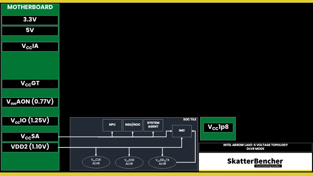
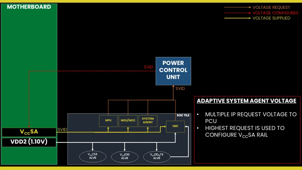
The most relevant parts powered by the VccSA voltage rail are the system agent, the NoC, the NPU, and the memory controller. The voltage configuration of the VccSA voltage rail is rather complicated. Since multiple IP domains share the voltage rail, the VccSA voltage is set based on the highest requested voltage from the various connected IP blocks.
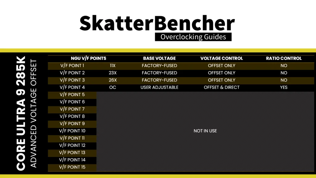
The NoC has its own V/F curve which is defined by up to four (4) V/F work points. The first three (3) V/F points (at 11X, 23X, and 26X) are factory-fused and the last point is mapped to the “OC Ratio.” Unfortunately, that’s as much as we can gather regarding the default V/F curve. It’s not easy to separate the NGU SVID request based on the VccSA behavior.
Based on the work points, the NGU requests an operating voltage from the VccSA voltage rail using the SVID protocol. However, there’s a second way to voltage configuration: ignore the SVID voltage requests and calculations, and program the VccSA voltage regulator directly over PMBus. This process effectively allows us to take full control over the voltage set by the VccSA voltage rail.
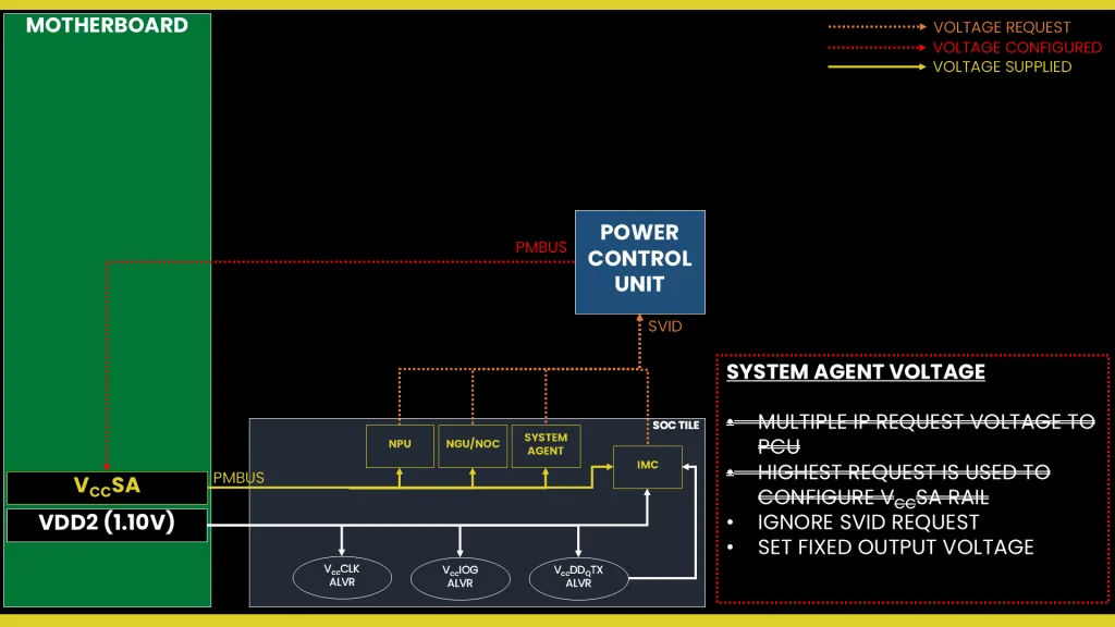
This approach is a very traditional way of overclocking whereby you set a fixed output voltage and then use an appropriate VRM load-line setting – if available – to reduce the operating voltage in higher load scenarios. The load-line configuration isn’t particularly useful for SA voltage rail.
D2D
D2D stands for Die-to-Die. It is the interface between the various tiles on the Arrow Lake package. There are three D2D links connecting the various tiles on the Arrow Lake package:
- SOC-Compute (H-IDI protocol) – P-core, E-core, Ring
- SOC-Graphics (CXL protocol) – Integrated Graphics
- SOC-IOE (PSF protocol) – IO extension
On Arrow Lake, only the SOC-Compute D2D can be overclocked. The base frequency is 2.1 GHz.
D2D Clocking Topology
The D2D reference clock frequency is generated internally by the SoC PLL. However, it can also be clocked with an external clock generator providing the reference clock for the SoC PLL. This clock affects nearly all the IP blocks of Arrow Lake, except for those in the Compute Tile and the PCIe/DMI links.


The reference clock is multiplied by the D2D ratio to achieve the final clock frequency. As said, we can only adjust the SOC-Compute D2D frequency. The default ratio is 21X, which yields a 2.1 GHz operating frequency. The maximum configurable ratio is 40X. The frequency can only be set at boot and cannot be changed in the operating system.
D2D Voltage Topology
The external 0.77V VnnAON voltage rail powers several internal voltages, including the D2D interfaces. The VnnAON voltage is pretty important for Arrow Lake CPUs as it is part of the voltage multiplexer for many IP blocks, including the cores and ring, typically serving as the floor voltage in power-saving scenarios.
I don’t suggest increasing it above 1.0V since it provides little additional benefit for overclocking and performance. Furthermore, increasing the VnnAON voltage can also cause issues when cold booting the system. Fortunately, ASUS has included an option called “High d2d cold boot workaround” in the BIOS that can help alleviate some of the booting issues with increased VnnAON voltages.
Data Fabric Tuning Process
Tuning the data fabric is a matter of testing each component systematically. I recommend first picking target voltages for each of the components and setting those in the BIOS with each component set to its default frequency. So:
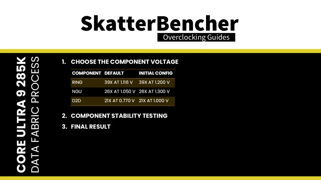
Then I increase the frequency for each component until I find instability. The initial tests can be very quick. For example, I’ll run a 30 second cycle of Y-Cruncher FFT Component tester to find the initial upper limit for each component.
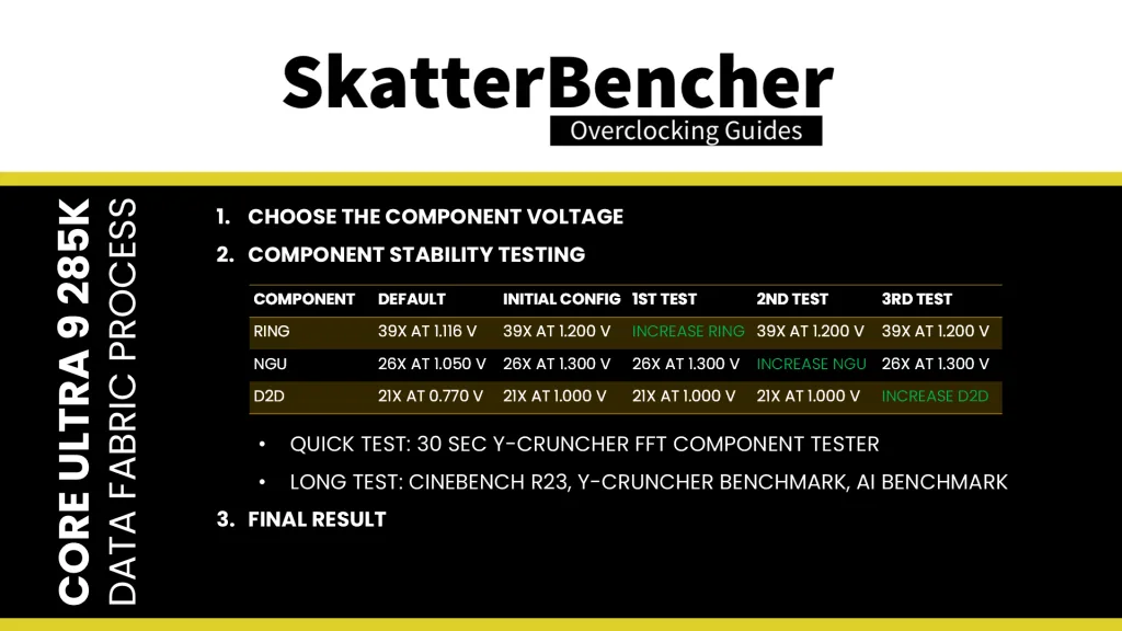
When I know the upper limit, I’ll set all target ratios and do longer stints of stability testing including the introduction of other tests. I find that, typically, Cinebench R23, Y-Cruncher Benchmark & Component Tester, and AI Benchmark are very sensitive to data fabric overclocking.
This process might take a bit longer, especially if you’re trying to find the maximum stable setting. When I’m satisfied with the stability testing, of course it also has to pass all the other benchmarks in our benchmark suite.
Ultimately, I ended up with a 4.2 GHz Ring, 3.4 GHz NGU, and 3.8 GHz D2D.
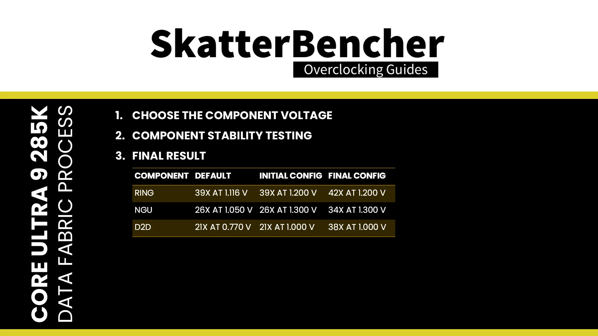
I want to emphasize a particular point regarding the Ring as I’ve received quite a number of questions about it. Don’t be surprised if you see extremely limited overclocking headroom for the Ring. It’s normal.
For the 285K, 4.2 GHz is within expectations. For the 245K, the Ring can be clocked a little higher as I demonstrated in SkatterBencher #83.
BIOS Settings & Benchmark Results
Upon entering the BIOS
- Go to the Extreme Tweaker menu
- Set Performance Preferences to ASUS Advanced OC Profile
- Set Ai Overclock Tuner to XMP I
- Set ASUS MultiCore Enhancement to Enabled – Remove All Limits
- Set Performance Core Ratio to By Core Usage
- Set 1-Core to 4-Core Ratio Limit to 57
- Set 5-Core and 6-Core Ratio Limit to 56
- Set 7-Core and 8-Core Ratio Limit to 55
- Enter the Specific Performance Core submenu
- Set Performance Core0 to Core5 Specific Ratio Limit to 56
- Set Performance Core6 and Core7 Specific Ratio Limit to 57
- Leave the Specific Performance Core submenu
- Set Efficient Core Ratio to By Core Usage
- Enter the By E-Core Usage submenu
- Set Efficient Turbo Ratio Limit 1 to 52
- Set Efficient Turbo Ratio Cores 1 to 8
- Set Efficient Turbo Ratio Limit 2 to 51
- Set Efficient Turbo Ratio Cores 2 to 12
- Set Efficient Turbo Ratio Limit 3 to 49
- Set Efficient Turbo Ratio Cores 3 to 16
- Leave the By E-Core Usage submenu
- Enter the Specific Efficient Core submenu
- Set Efficient Core Group0 Specific Ratio Limit to 51
- Set Efficient Core Group1 to Group3 Specific Ratio Limit to 52
- Leave the Specific Efficient Core submenu
- Set DRAM Frequency to DDR5-8000
- Enter the Thermal Velocity Boost submenu
- Set TVB Voltage Optimizations to Disabled
- Set Overclocking TVB to Enabled
- Set OC TVB Configuration Limit to Per P-core Group
- Set OC TVB Ratio Item Mode to All Core Mode
- Set All core to Enabled
- Set Negative Ratio Offset A to 0
- Set Negative Ratio Offset B to 0
- Leave the Thermal Velocity Boost submenu
- Enter the Performance Core V/F Point Offset submenu
- Set V/F Point Present Mode to All Core Mode
- Set V/F Point Voltage Control Mode to Manual Mode
- Leave the Performance Core V/F Point Offset submenu
- Enter the Efficient Core V/F Point Offset submenu
- Set V/F Point Present Mode to All Core Mode
- Set V/F Point Voltage Control Mode to Manual Mode
- Leave the Efficient Core V/F Point Offset submenu
- Enter the Tweaker’s Paradise submenu
- Set High d2d cold boot workaround to Enabled
- Leave the Tweaker’s Paradise submenu
- Set Max. CPU Cache Ratio to 42
- Set NGU Ratio to 34
- Set CPU D2D Ratio to 38
- Set Performance Core DLVR Voltage to Adaptive Mode
- Set Additional Turbo mode Voltage to 0.600
- Set Efficient Core DLVR Voltage to Adaptive Mode
- Set Additional Turbo mode Voltage to 1.250
- Set Ring DLVR Voltage to Adaptive Mode
- Set Additional Turbo mode Voltage to 1.200
- Set CPU System Agent Voltage to Manual Mode
- Set CPU System Agent Voltage Override to 1.300
- Set VNNAON 0.77v Voltage to Manual Mode
- Set VNNAON Voltage Override to 1.000
Then save and exit the BIOS.
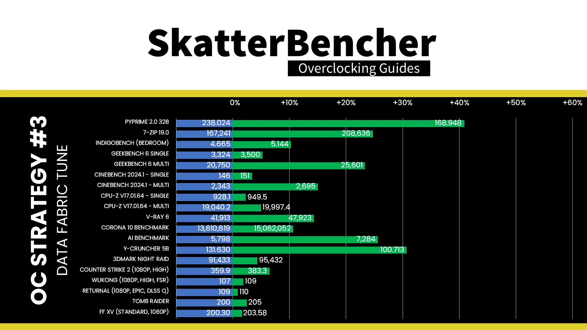
We re-ran the benchmarks and checked the performance increase compared to the default operation.
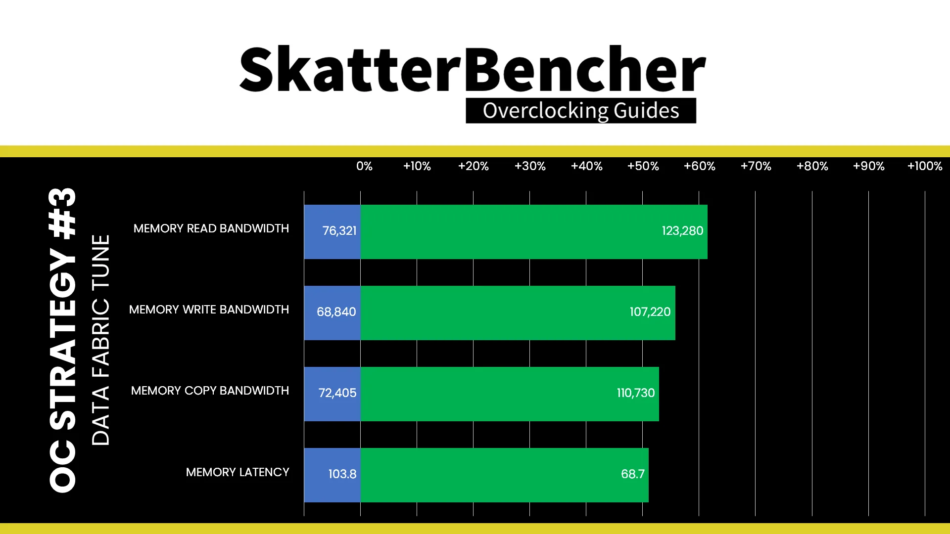
The multi-tile Arrow Lake architecture adds some layers of communication between the system memory and CPU cores. By increasing the frequency of the Ring, NGU, and D2D, we aim to increase the data transfer speed. We can see that the performance improves accordingly, especially in memory-sensitive workloads. The Geomean performance improves by another 1.23 percentage points, and we get a maximum improvement of +40.89% in PyPrime.
OC Strategy #4: CPU Core Finetuning
In our fourth overclocking strategy, I try to squeeze more performance out of the CPU cores by exploring all the tuning technologies available for Arrow Lake. That includes granular ratios, voltage limit override, overclocking thermal velocity boost, and advanced voltage offset.
Voltage Limits
To safeguard the processor, for the first time, Intel imposes strict voltage limits for several IP blocks, including the P-cores and E-cores. This voltage limit effectively prevents the cores from requesting a higher voltage from the PCU.
By default, the voltage limit for the P-cores and E-cores is +200 mV above the lowest VID for the P-cores’ V/F Point 8 and E-core’s V/F Point 6. For this CPU’s P-cores, that’s 1.381V + 200 mV = 1.581V and for the E-cores it’s 1.070 V + 200mV = 1.270V. However, we can manually increase that to +300 mV under ambient conditions, so 1.681V and 1.370V respectively.
If you try setting the limit above the approved limit, the PCU will automatically adjust it to the highest allowed limit. If you disable voltage limits and the temperature is above 10 degrees Celsius, the CPU will operate in “safe mode” and limit the frequency to 400 MHz.
Granular Ratios
Granular Ratios are a brand-new overclocking feature for Arrow Lake. It adjusts the Per Core Ratio Limit by letting you set the CPU frequency in steps of 16.67 and 33.33 MHz. The granular ratios can only be configured in reference to the Per Core Ratio Limit, not as a Turbo Ratio limit. That’s because, technically, the granular ratios aren’t set directly but instead “down-binned” from the Per Core Ratio Limit.
For example, let’s say you set a granular ratio of 60.16X. In that case, the Per Core Ratio Limit is set to 61X and then “down-binned” by 5 steps of 16.67 MHz (100 MHz divided by 6). That is important to keep in mind in case you’re also using other ratio configuration technologies.
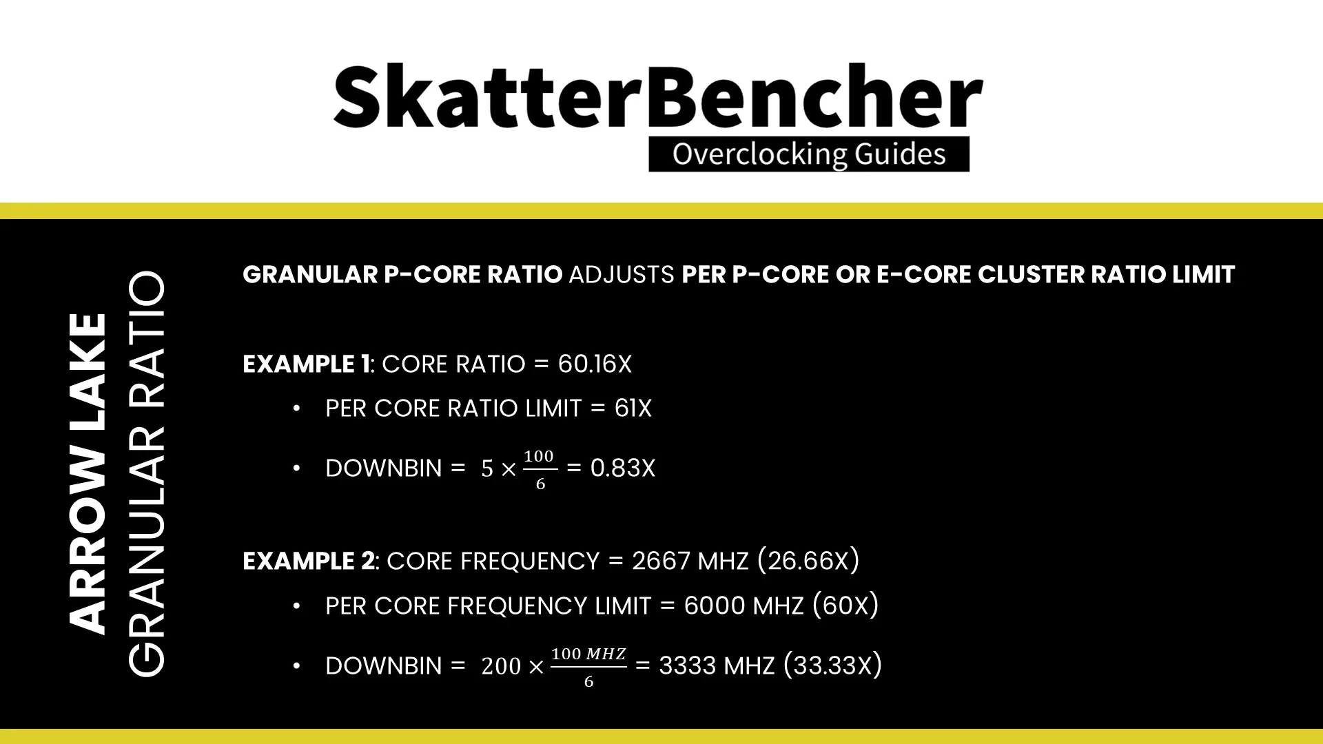
It’s also important to keep in mind when using adaptive voltage mode, because the adaptive voltage maps to the “OC Ratio.” In our previous example, where we use a 60.16X granular ratio, let’s say we also set an adaptive voltage of 1.45V. In this case, the adaptive voltage maps to 61X and also applies to any ratio between 60X and 61X.
OverClocking Thermal Velocity Boost
In OC Strategy #2 I already touched on OverClocking Thermal Velocity Boost. In short, this technology allows us to down-bin the Turbo Ratio Limit depending on the CPU’s operating temperature. Basically, when the CPU temperature exceeds a threshold, the Turbo Ratio Limit can be reduced.
In practice, this tool is very helpful in managing instabilities at high frequencies in all core workloads. Specifically, I found that the P-cores can run at 5.6 GHz in light all-core workloads but would crash when running heavier workloads.
So, by setting an OCTVB down-bin of 1 for when 7 or more P-cores are active at a temperature of 70 degrees or higher, I get the best of both worlds: 5.6 GHz for all-cores in light workloads and 5.5 GHz when the workload gets too tough.
Advanced Voltage Offset
Advanced Voltage Offset, more commonly known as V/F Points, is available for each of the P-cores and each of the E-core clusters. There are nine (9) available VF Points for each P-core, eight of which are fixed to a specific ratio. That ratio is the same for all P-cores. There are seven (7) available VF Points for each E-core cluster, six of which are fixed to a specific ratio. That ratio is the same for all E-core clusters.
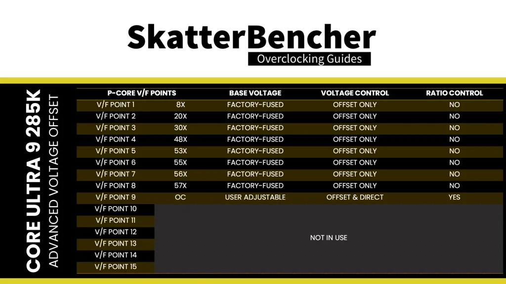
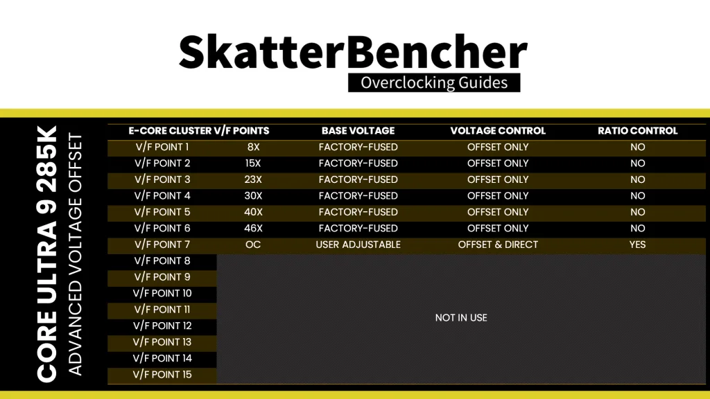
The final VF Point is mapped to the “OC Ratio” which is the P-core or E-core Cluster Per Core Ratio Limit. If you use granular ratios, keep in mind those are down-binned from the next full ratio. In other words, the OC Ratio cannot be a granular ratio!
You can set a negative or positive voltage offset for each of these V/F points. The final OC ratio’s base voltage will be the user-configured adaptive voltage. I’ll cover how I used the V/F Points for this particular CPU in a couple of minutes.
Arrow Lake P-core and E-core Finetuning Discussion
As we discussed in OC Strategy #2 – tuning the Arrow Lake CPU cores is not without a struggle. Fortunately, Intel’s CPU overclocking toolkit is by far the most comprehensive tuning toolkit available for enthusiasts. So, even if we can’t get the frequencies up by much, it’s not for a lack of tools.
I approach the fine-tuning similarly as the basic tuning: voltage first, then 1T stability, and lastly all-core stability.
Choosing the Voltage
From earlier testing, it’s clear that the P-cores don’t scale much with voltage beyond the maximum default frequency of 5.7 GHz. That said, I still increase the voltage at V/F Point 8 (which is for the 57X ratio) by 50mV in the hope to push the non-favored P-cores closer to the 5.7 GHz mark.
For the E-cores, I first increase the Voltage Limit to its maximum allowed limit, and then increase the adaptive voltage to 1.35V. That’s 100mV more than what we used in OC Strategy #2.
1T Stability
I follow a similar testing process and benchmark selection as in OC Strategy #2. The main difference is that there’s a bit more finessing involved when you’re near the maximum overclock. The limiting factor remains the same: AI Benchmark is not stable with high P-core frequencies.
By offsetting the P-core V/F Point 8 with an extra 50mV, we increase the voltage at 57X for every P-core. That gives us enough headroom to further increase the non-favored P-cores to 5683 MHz and the two favored P-cores to 5716 MHz.
I want to emphasize two things about this configuration
- Remember the rules for Granular Ratios: the ratio is down-binned from the Per Core Ratio Limit. So, when we set 56.83X for the non-favored P-cores, it’s running at the voltage mapped to 57X which we increased by offsetting at V/F Point 8.
- Remember the rules for Adaptive Voltage: the voltage for the favored P-cores running at 57.16X is defined by the 58X ratio. That’s mapped to V/F Point 9, which we configured by setting the global adaptive voltage to 0.6V. Since 0.6V is below the voltage for V/F Point 8, the voltage for 57.16X will be the same as for 57X.
The additional 100mV gives us another 100 MHz for the E-cores. One of the E-core clusters seems a little better than the others and can run 5.3 GHz at lower voltage. By setting its Per Core Ratio Limit to 54X, I can lower the effective voltage at 5.3 GHz. Alternatively, I could have configured the Per Core Adaptive Voltage.
nT Stability
To improve the frequency in heavy all-core workloads, I use two distinct technologies: advanced voltage offset and overclocking thermal velocity boost.
The Advanced Voltage Offset lets me undervolt the P-cores and E-cores in all-core workloads. The E-cores in particular could undervolt quite significantly at V/F Point 6, which matches 46X. By lowering the voltage by 75mV, I we negate some of the effects of increasing the adaptive voltage to 1.35V.
The P-core undervolting headroom is a lot less impressive. Still, I was able to reduce V/F Point 5, mapped to 53X, by 50mV, and V/F Point 6, mapped to 55X, by 15mV.
The last thing I did was use OCTVB to reduce the P-core frequency in all-core workloads by 1 bin from 56X to 55X when the temperature exceeds 70 degrees Celsius. This was necessary because I could run 56X in lighter workloads but it would crash in heavy workloads.
Final Result
The final fine-tune is quite a complicated overclock where we get 5717 MHz for the favored P-cores and up to 5.6 GHz when all P-cores are active and running below 70 degrees Celsius. The E-cores can boost to 5.3 GHz and hit 5.0 GHz in all-core workloads.
BIOS Settings & Benchmark Results
Upon entering the BIOS
- Go to the Ai Tweaker menu
- Set Performance Preferences to ASUS Advanced OC Profile
- Set Ai Overclock Tuner to XMP I
- Set ASUS MultiCore Enhancement to Enabled – Remove All Limits
- Set Performance Core Ratio to By Core Usage
- Set 1-Core to 6-Core Ratio Limit to 58
- Set 7-Core and 8-Core Ratio Limit to 56
- Enter the Specific Performance Core submenu
- Set Performance Core0 to Core5 Specific Ratio Limit to 56.83
- Set Performance Core6 and Core7 Specific Ratio Limit to 57.17
- Leave the Specific Performance Core submenu
- Set Efficient Core Ratio to By Core Usage
- Enter the By E-Core Usage submenu
- Set Efficient Turbo Ratio Limit 1 to 53
- Set Efficient Turbo Ratio Cores 1 to 4
- Set Efficient Turbo Ratio Limit 2 to 52
- Set Efficient Turbo Ratio Cores 2 to 12
- Set Efficient Turbo Ratio Limit 3 to 50
- Set Efficient Turbo Ratio Cores 3 to 16
- Leave the By E-Core Usage submenu
- Enter the Specific Efficient Core submenu
- Set Efficient Core Group0, Group2, and Group3 Specific Ratio Limit to 53
- Set Efficient Core Group1 Specific Ratio Limit to 54
- Leave the Specific Efficient Core submenu
- Set DRAM Frequency to DDR5-8000
- Enter the Thermal Velocity Boost submenu
- Set TVB Voltage Optimizations to Disabled
- Set Overclocking TVB to Enabled
- Set OC TVB Configuration Limit to Per P-core Group
- Set OC TVB Ratio Item Mode to Per Core Mode
- Set 7- and 8-Core Active to Enabled
- For 7- and 8-Core Active, set Temperature A to 70
- For 7- and 8-Core Active, set Negative Ratio Offset to 1
- Leave the Thermal Velocity Boost submenu
- Enter the Max Voltage Limits submenu
- Set E-Core Max Voltage Limits to 1.361
- Leave the Max Voltage Limits submenu
- Enter the Performance Core V/F Point Offset submenu
- Set V/F Point Present Mode to Per Core Mode
- For Performance Core 0 to 5 V/F Point Offset,
- Set V/F Point 5 Offset to -50
- Set V/F Point 6 Offset to -15
- Set V/F Point 8 Offset to +50
- For Performance Core 6 and 7 V/F Point Offset,
- Set V/F Point 5 Offset to -50
- Set V/F Point 6 Offset to -15
- Leave the Performance Core V/F Point Offset submenu
- Enter the Efficient Core V/F Point Offset submenu
- Set V/F Point Present Mode to All Core Mode
- Set V/F Point Voltage Control Mode to Manual Mode
- Set V/F Point 6 Offset to -75
- Leave the Efficient Core V/F Point Offset submenu
- Enter the Tweaker’s Paradise submenu
- Set High d2d cold boot workaround to Enabled
- Leave the Tweaker’s Paradise submenu
- Set Max. CPU Cache Ratio to 42
- Set NGU Ratio to 34
- Set CPU D2D Ratio to 38
- Set Performance Core DLVR Voltage to Adaptive Mode
- Set Additional Turbo mode Voltage to 0.600
- Set Efficient Core DLVR Voltage to Adaptive Mode
- Set Additional Turbo mode Voltage to 1.250
- Set Ring DLVR Voltage to Adaptive Mode
- Set Additional Turbo mode Voltage to 1.200
- Set CPU System Agent Voltage to Manual Mode
- Set CPU System Agent Voltage Override to 1.300
- Set VNNAON 0.77v Voltage to Manual Mode
- Set VNNAON Voltage Override to 1.000
Then save and exit the BIOS.
The CPU boost frequency with 1 active P-core is 5716 MHZ. The average boost frequency gradually trails off to 5600 MHz when all P-cores are active and to 5200 MHz when all P- and E-cores are active. In single-threaded applications, two P-cores can boost to 5716 MHz and six can boost up to 5683 GHz. Every E-core can boost to 5.3 GHz.
We re-ran the benchmarks and checked the performance increase compared to the default operation.

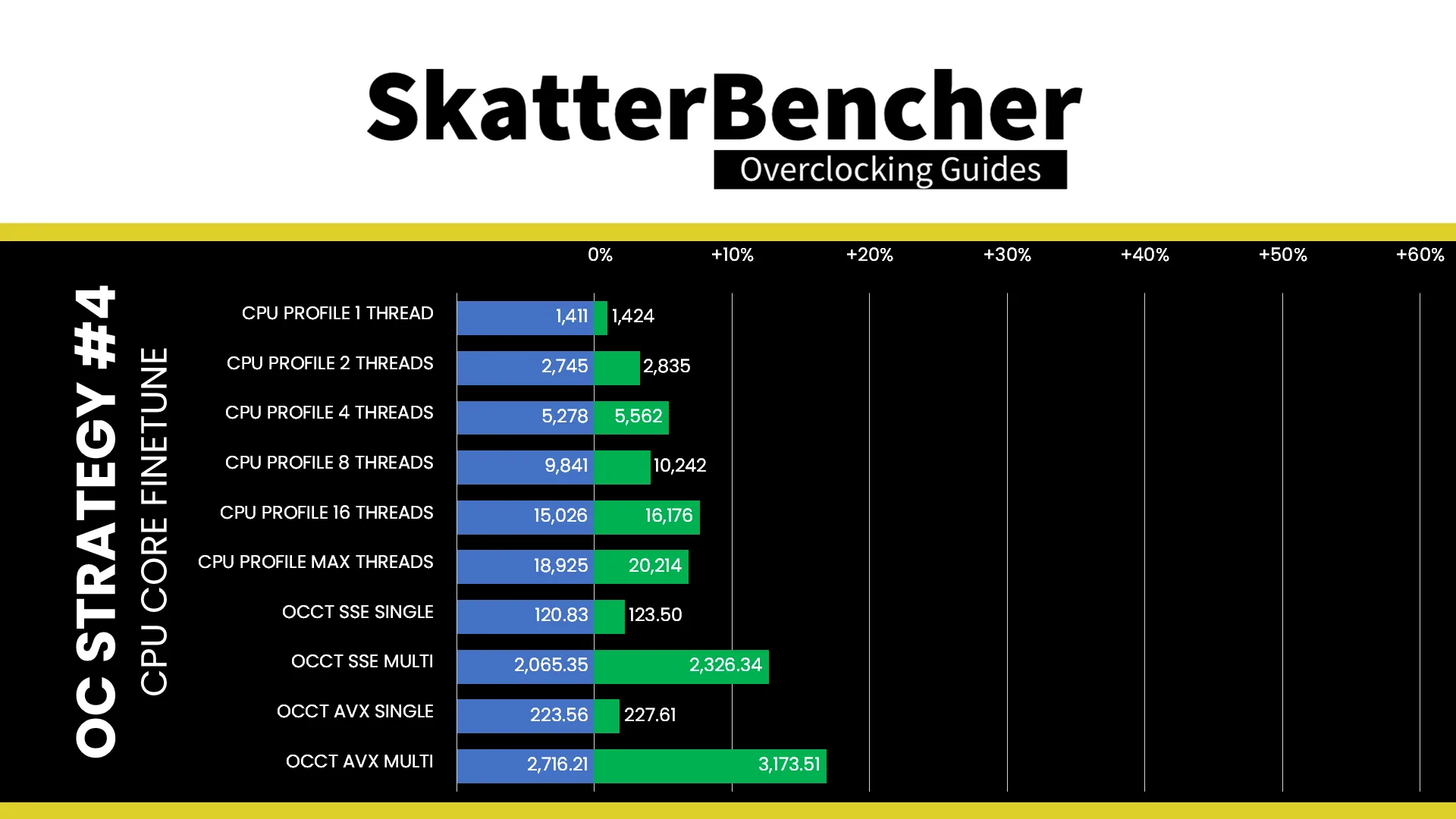

While the additional voltage doesn’t add much P-core top speed, the additional 100 to 200 MHz for the E-cores and the undervolt for P-cores and E-cores helps lift the performance in multi-threaded workloads. The Geomean performance improves by another 0.57 percentage points, and we get a maximum improvement of +40.51% in PyPrime.
When running the OCCT CPU AVX2 Stability Test, the average CPU P-core effective clock is 5455 MHz with 1.216 volts and the average CPU E-core effective clock is 5001 MHz with 1.199 volts. The average CPU temperature is 104.0 degrees Celsius. The average CPU package power is 369.6 watts.
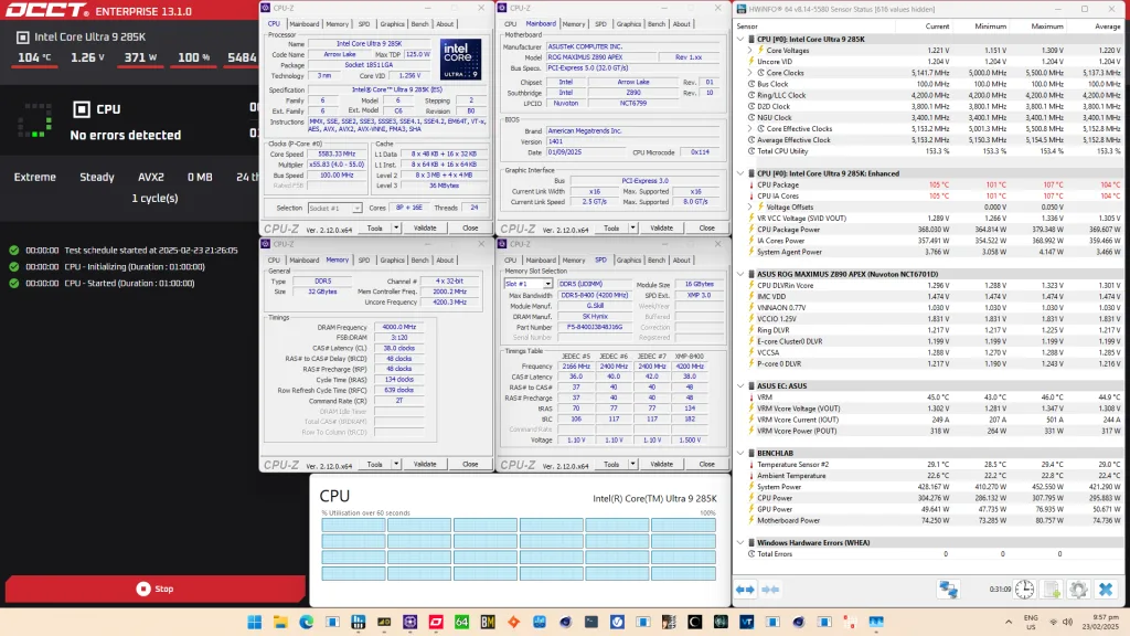
When running the OCCT CPU SSE Stability Test, the average CPU P-core effective clock is 5419 MHz with 1.218 volts and the average CPU E-core effective clock is 5000 MHz with 1.219 volts. The average CPU temperature is 103.0 degrees Celsius. The average CPU package power is 365.3 watts.

OC Strategy #5: DRAM Tuned
In our fifth overclocking strategy, we try to tune the memory sub system and adjust the DRAM timings to see if it has any impact on system performance. For this I rely on the ASUS Memory Presets and manual timing adjustments.
Memory Presets
ASUS Memory Presets is an ASUS overclocking technology that provides you with a selection of memory tuning presets for certain memory ICs. The presets will adjust the memory timings and voltages.
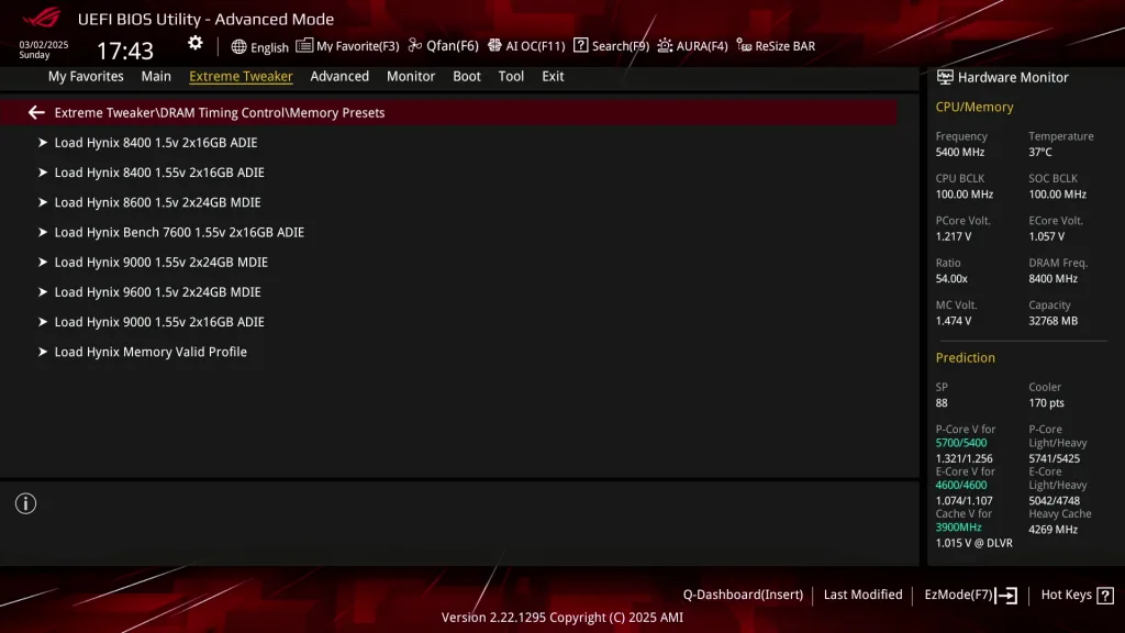
On the ASUS ROG Z890 Apex motherboard (BIOS 1401) there are 8 presets available for Hynix 2x16GB and 2x24GB memory. Since I’ll be looking to improve the memory timings as well as maybe increase the memory frequency, I load the Hynix 9000 1.55v 2x16GB ADIE profile.
Here is the configuration of that profile:
Memory Preset
Motherboard	ASUS ROG Maximus Z890 Apex
BIOS		1401
Preset		Hynix 8400 1.5v 2x16GB ADIE

Voltage
DRAM VDD	1.55
DRAM VDDQ	1.55

Primary Timings
tCL		40
tRCD 		53
tRCDWR		53
tRP 		53
tRAS		55

Secondary Timings
tRRD_sg		12
tRRD_dg		8
tRFC		650
tRFCsb		650
tREFI		131071
tWR		Auto
tRTP		14
tFAW		24
tCCD_L_WR	36
tWCL		38

Tertiary Timings
tRDRD_sg	17
tRDRD_dg	8
tRDWR_sg	20
tRDWR_dg	20
tWRWR_sg	30
tWRWR_dg	8
tWRRD_sg	68
tWRRD_dg	54
tRDRD_dr	10
tRDRD_dd	10
tRDWR_dr	15
tRDWR_dd	15
tWRWR_dr	13
tWRWR_dd	13
tWRRD_dr	7
tWRRD_dd	7
tCCD_L_tDLLK	12
DRAM Tuning
It’s of course not a given that copying over timings will work with any 2x16GB Hynix kit. So, to start the tuning I first try the same DDR5-8000 frequency with the new memory timings and check if it boots and is stable.
Testing for memory stability is a bit of a hot topic in the enthusiast community as there are several yardsticks used by different communities. If I’m not mistaken, Karhu is the current meta, but I’ve always relied on 1h of OCCT Memory Stress Test. But if you prefer a different stress test, that’s OK too. At the end of the day, stability means different things to different people.
Then, I tried to increase the frequency to DDR5-8600. To achieve stability, I had to adjust a couple of memory timings:
- DRAM RAS# to RAS# Delay L from 12 to 16
- DRAM Refresh Interval from 131071 to 32768
- DRAM Write Recovery Time from Auto to 66
- tRDWR_sg & tRDWR_dg from 20 to 24
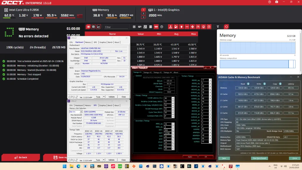
Here is my final memory configuration:
Memory Kit
VENDOR G.SKILL
SKU F5-8400J3848J16G
DRAM IC Hynix A-DIE
PMIC Richtek
Frequency
MCLK 4300 (DDR5-8600)
IMCCLK 2150
Voltage
VccSA 1.30
DRAM VDD 1.55
DRAM VDDQ 1.55
Primary Timings
tCL 40
tRCD 53
tRCDWR 53
tRP 53
tRAS 55
Secondary Timings
tRRD_L 16
tRRD_S 8
tRFC 650
tRFCsb 650
tREFI 32768
tWR 66
tRTP 14
tFAW 24
tCCD_L_WR 36
tWCL 38
Tertiary Timings
tRDRD_sg 17
tRDRD_dg 8
tRDWR_sg 24
tRDWR_dg 24
tWRWR_sg 30
tWRWR_dg 8
tWRRD_sg 68
tWRRD_dg 54
tRDRD_dr 10
tRDRD_dd 10
tRDWR_dr 15
tRDWR_dd 15
tWRWR_dr 13
tWRWR_dd 13
tWRRD_dr 7
tWRRD_dd 7
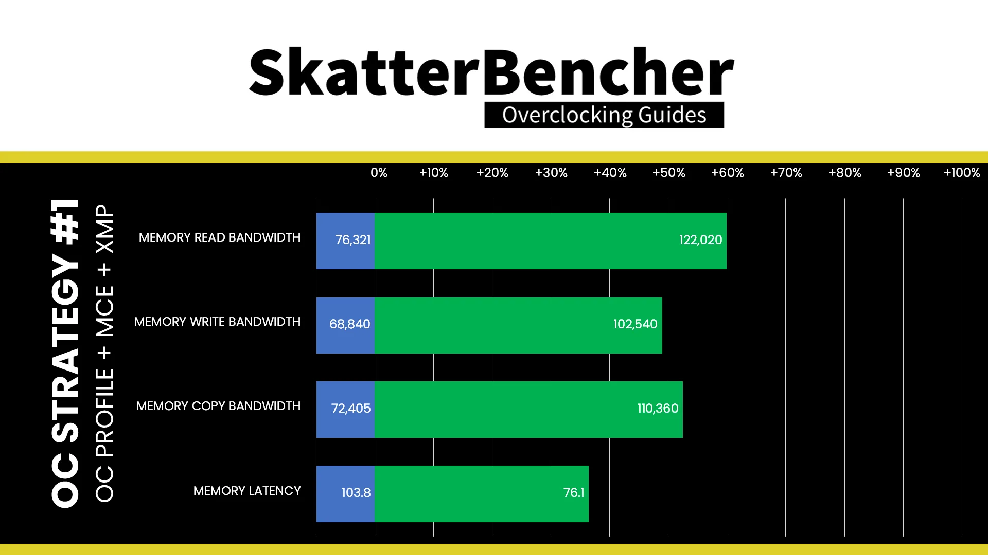
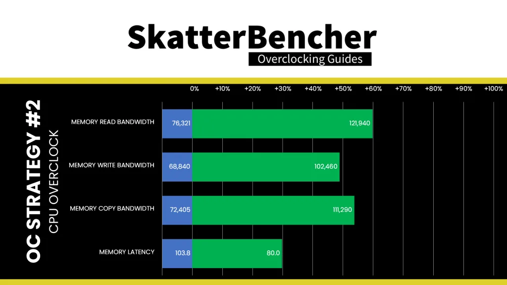
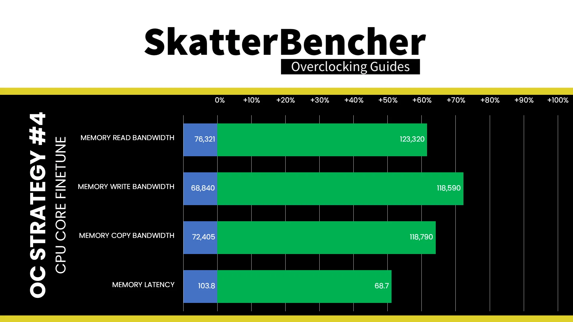
tCCD_L_tDLLK 12After the tuning, our AIDA64 performance improved quite significantly. We got about +60% extra bandwidth and +25% better latency enabling XMP-8000. Tuning the data fabric improves the write bandwidth by 17% and improved the latency by 7%. The tuned memory then adds another 12% extra write and copy bandwidth while maintaining the same latency.

BIOS Settings & Benchmark Results
Upon entering the BIOS
- Go to the Ai Tweaker menu
- Set Performance Preferences to ASUS Advanced OC Profile
- Set Ai Overclock Tuner to XMP I
- Set ASUS MultiCore Enhancement to Enabled – Remove All Limits
- Set Performance Core Ratio to By Core Usage
- Set 1-Core to 6-Core Ratio Limit to 58
- Set 7-Core and 8-Core Ratio Limit to 56
- Enter the Specific Performance Core submenu
- Set Performance Core0 to Core5 Specific Ratio Limit to 56.83
- Set Performance Core6 and Core7 Specific Ratio Limit to 57.17
- Leave the Specific Performance Core submenu
- Set Efficient Core Ratio to By Core Usage
- Enter the By E-Core Usage submenu
- Set Efficient Turbo Ratio Limit 1 to 53
- Set Efficient Turbo Ratio Cores 1 to 4
- Set Efficient Turbo Ratio Limit 2 to 52
- Set Efficient Turbo Ratio Cores 2 to 12
- Set Efficient Turbo Ratio Limit 3 to 50
- Set Efficient Turbo Ratio Cores 3 to 16
- Leave the By E-Core Usage submenu
- Enter the Specific Efficient Core submenu
- Set Efficient Core Group0, Group2, and Group3 Specific Ratio Limit to 53
- Set Efficient Core Group1 Specific Ratio Limit to 54
- Leave the Specific Efficient Core submenu
- Set DRAM Frequency to DDR5-8600
- Enter the DRAM Timing Control submenu
- Enter the Memory Presets submenu
- Load the Hynix 9000 1.55v 2x16GB ADIE profile
- Leave the Memory Presets submenu
- Set DRAM RAS# to RAS# Delay L to 16
- Set DRAM Refresh Interval to 32768
- Set DRAM Write Recovery Time to 66
- Set tRDWR_sg and tRDWR_dg to 24
- Enter the Memory Presets submenu
- Leave the DRAM Timing Control submenu
- Enter the Thermal Velocity Boost submenu
- Set TVB Voltage Optimizations to Disabled
- Set Overclocking TVB to Enabled
- Set OC TVB Configuration Limit to Per P-core Group
- Set OC TVB Ratio Item Mode to Per Core Mode
- Set 7- and 8-Core Active to Enabled
- For 7- and 8-Core Active, set Temperature A to 70
- For 7- and 8-Core Active, set Negative Ratio Offset to 1
- Leave the Thermal Velocity Boost submenu
- Enter the Max Voltage Limits submenu
- Set E-Core Max Voltage Limits to 1.361
- Leave the Max Voltage Limits submenu
- Enter the Performance Core V/F Point Offset submenu
- Set V/F Point Present Mode to Per Core Mode
- For Performance Core 0 to 5 V/F Point Offset,
- Set V/F Point 5 Offset to -50
- Set V/F Point 6 Offset to -15
- Set V/F Point 8 Offset to +50
- For Performance Core 6 and 7 V/F Point Offset,
- Set V/F Point 5 Offset to -50
- Set V/F Point 6 Offset to -15
- Leave the Performance Core V/F Point Offset submenu
- Enter the Efficient Core V/F Point Offset submenu
- Set V/F Point Present Mode to All Core Mode
- Set V/F Point Voltage Control Mode to Manual Mode
- Set V/F Point 6 Offset to -75
- Leave the Efficient Core V/F Point Offset submenu
- Enter the Tweaker’s Paradise submenu
- Set High d2d cold boot workaround to Enabled
- Leave the Tweaker’s Paradise submenu
- Set Max. CPU Cache Ratio to 42
- Set NGU Ratio to 34
- Set CPU D2D Ratio to 38
- Set Performance Core DLVR Voltage to Adaptive Mode
- Set Additional Turbo mode Voltage to 0.600
- Set Efficient Core DLVR Voltage to Adaptive Mode
- Set Additional Turbo mode Voltage to 1.250
- Set Ring DLVR Voltage to Adaptive Mode
- Set Additional Turbo mode Voltage to 1.200
- Set CPU System Agent Voltage to Manual Mode
- Set CPU System Agent Voltage Override to 1.300
- Set VNNAON 0.77v Voltage to Manual Mode
- Set VNNAON Voltage Override to 1.000
Then save and exit the BIOS.
We re-ran the benchmarks and checked the performance increase compared to the default operation.
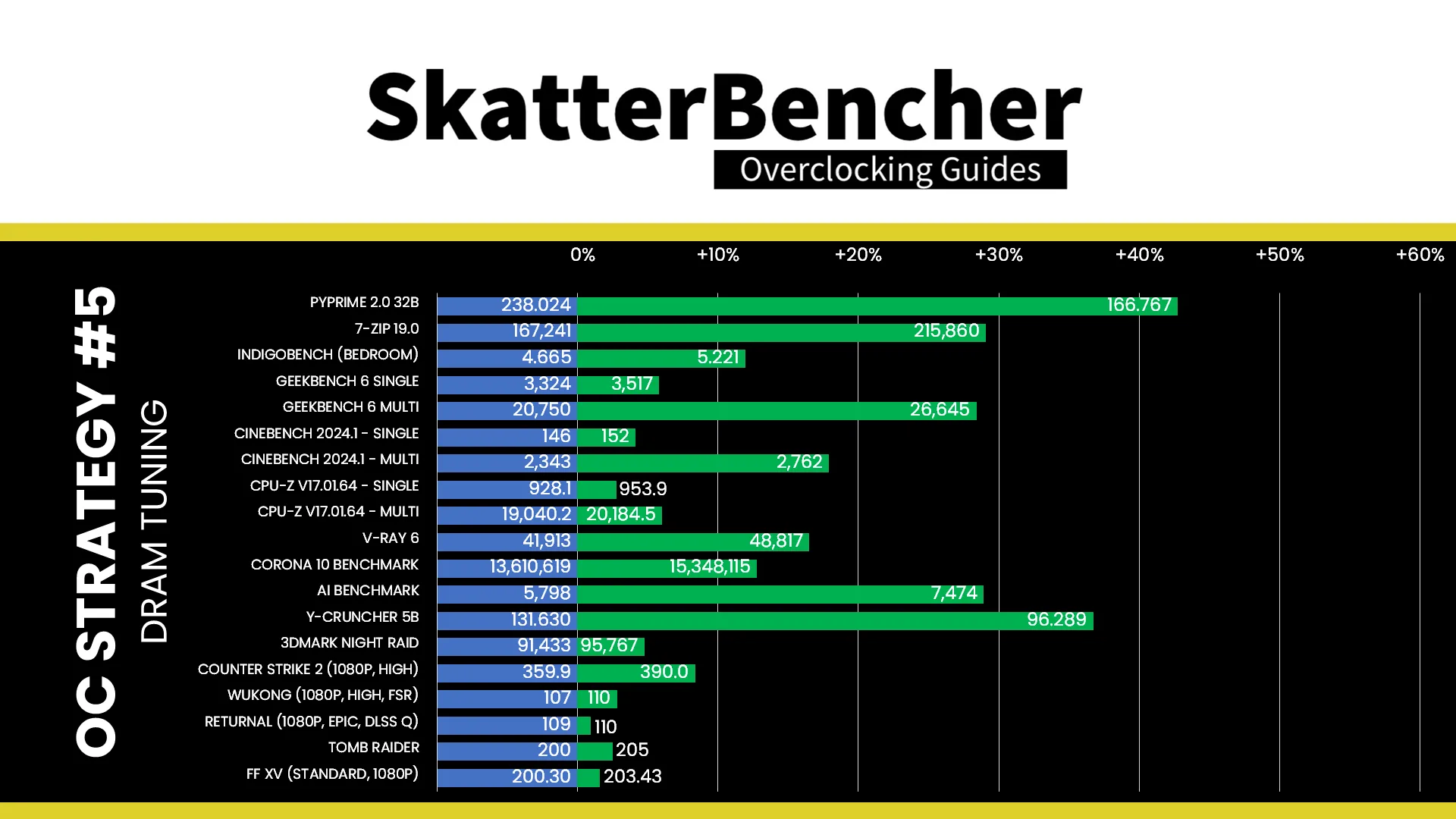
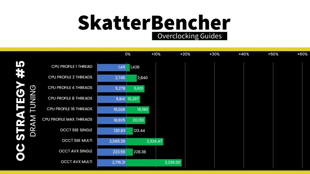

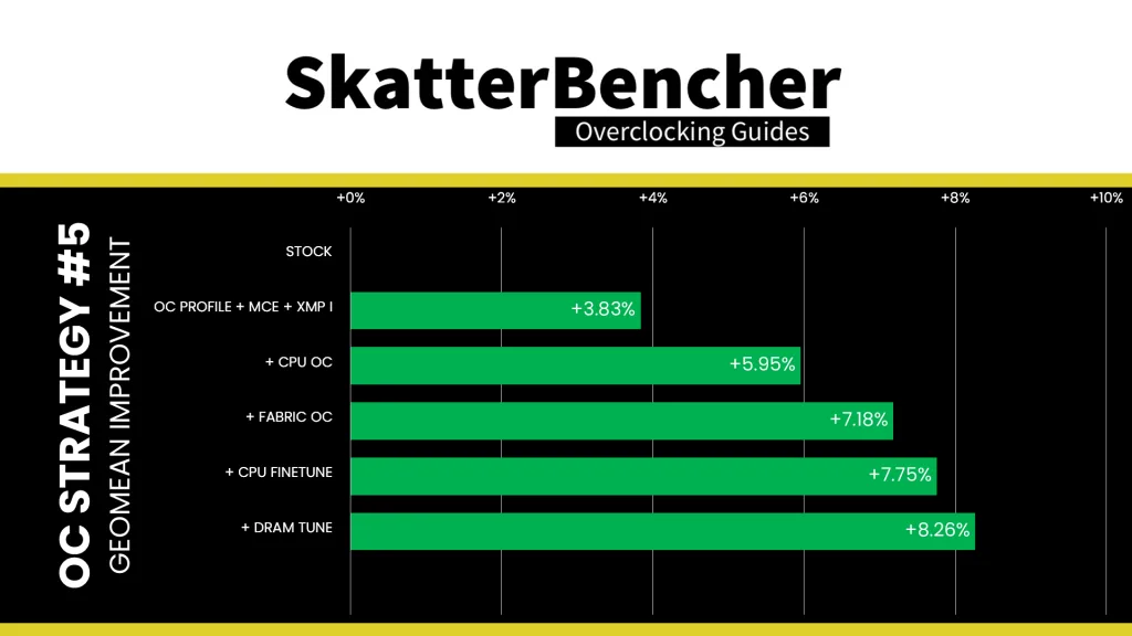
Tuning the memory timings and adding a little bit of frequency doesn’t have the enormous impact some would expect. However, it’s nonetheless interesting to still see performance improve, especially in multi-threaded workloads. The Geomean performance improves by another half a percentage point, and we get a maximum improvement of +42.73% in PyPrime.
OC Strategy #6: Power Gate Mode
In our final overclocking strategy, we explore Power Gate Mode and see if it can improve our CPU core overclock.
VccIA Power Gate SVID Mode
In Power Gate Mode, all the DLVRs tied to the VccIA voltage rail are bypassed and the connected IP blocks are powered directly by the VccIA voltage rail. That includes the P-cores, E-core clusters and their cache, the Ring, and the last-level cache.
Power Gate mode is basically how the VccIA rail worked on previous generation Raptor Lake processors. For Arrow Lake, it works … but it’s a little complicated.
To make a long story short: when the P-cores, E-cores, and Ring request their voltage to the CPU PCU, they account for a ton of other compensations including voltage droop, AVX Guardband, Thermal Velocity Boost voltage optimizations, etc. The result is that the actual voltage provided from the VccIA voltage rail to the IP blocks is relatively high!
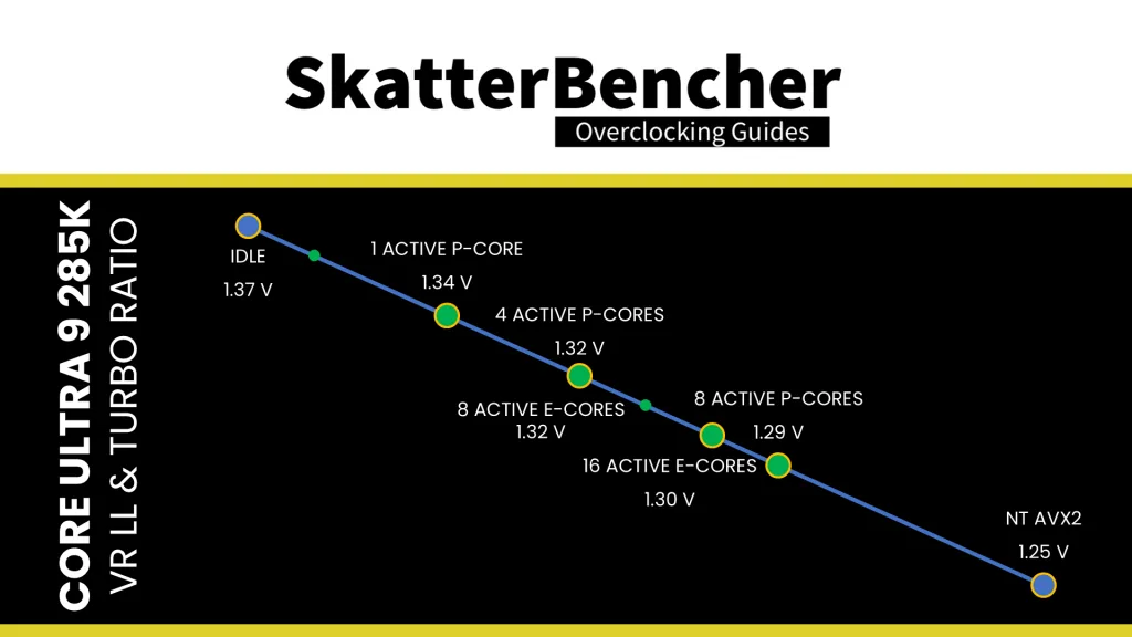
For example, here are the voltages with an Arrow Lake CPU running a light all-core workload.
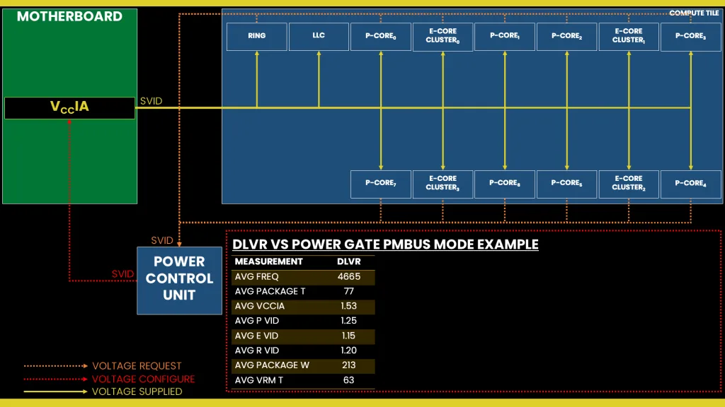
We can interpret this as follows: the P-core, E-core, and Ring request a voltage to the PCU to ensure it’ll run at 1.15V, 1.05V, and 1.1V respectively. The PCU then adds compensation for the load-lines, CEP, TVB, AVX, AC LL, DLVR efficiency losses, etc. At the end of the calculation, the PCU determines the VccIA voltage rail should provide 1.43V input voltage to the DLVRs.
If we were to switch to Power Gate mode but maintain the same mechanism for calculating the required voltage, then the VccIA voltage rail would effectively provide 1.43V to the P-cores, E-cores, and Ring. That’s obviously way too high and would quickly result in an overheating system. But this would be how voltage was configured on previous-generation Raptor Lake processors.
VccIA Power Gate PMBus Mode
Fortunately, there’s another way to approach Power Gate Mode voltage configuration: ignore the SVID voltage requests and calculations, and program the VccIA voltage regulator directly using PMBus. This process effectively allows us to take full control over the voltage set by the VccIA voltage rail.
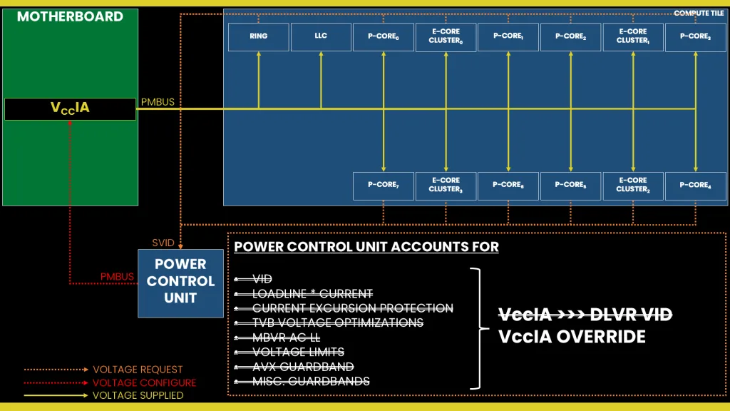
This approach is a very traditional way of overclocking whereby you set a fixed output voltage and use an appropriate VRM load-line setting to reduce the operating voltage in higher load scenarios.
Let’s have a look at how the tuning process looks.
Power Gate Mode Banned
But before we continue, we must talk about the elephant in the room: Power Gate Mode will not be available for ambient overclocking in the future. Or at the very least, that’s Intel’s plan.
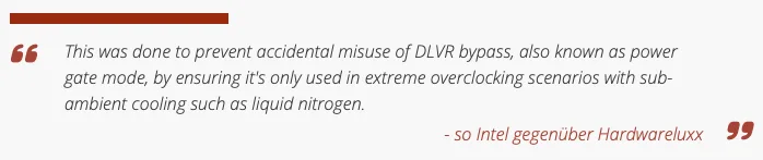
The real reason is not known but it’s probably got something to do with Power Gate Mode enabling voltages much higher than the DLVR limits. That could – in theory – cause harm to the CPU.
My opinion on this matter is clear: just like anything related to overclocking, enabling Power Gate Mode is not in-spec behavior, voids the warranty, and may cause damage to your processor. The decision whether to accept the risk should be up to the customer that purchased the product, not Intel. I don’t need someone sitting in an office cubicle far removed from my workspace to tell me what I can and cannot do with the hardware I paid for.
With that out of the way, I also want to briefly touch on why Power Gate Mode is still available on some motherboards with newer BIOSes. To keep it short: while the latest firmware package from Intel doesn’t officially allow for Power Gate mode to be enabled, since it was available on older code it’s possible for motherboard vendors to rely on older firmware to retain support.
Think of it like the support for non-K overclocking or AVX512 on Alder Lake processors. Similarly, motherboard vendors can re-use older dCode firmware to continue PG Mode support.
Power Gate Mode Tuning
The tuning process with Power Gate is similar to what we did in OC Strategy #2 and #4, with one major difference. Instead of relying on the CPU V/F curve, we override it with a static voltage and control the voltage under high load with an appropriate VR load-line.
Choosing the Voltage
The easiest way to choose an appropriate VccIA voltage for Power Gate mode is by first choosing the maximum voltage for 1T workloads and then afterwards configuring a VR load-line to stabilize nT workloads.
For my system, I picked 1.375V for the VccIA voltage. The reasoning is that this is about the Vlimit for the E-cores, and I wanted to see what we can from a system if Power Gate mode were officially allowed but with strict enforcement of the voltage limits.
First , we test 1T stability.
1T Stability
Similar to what we did in OC Strategy #2, we can first set the Turbo Ratio Limit to a high enough value (like 60X), then use the Per Core Ratio Limit to check stability for each P-core and E-core cluster.
With 1.375V static voltage for the P-cores, I could increase all except one P-core to 5.8 GHz. However, that’s only possible if I make extensive use of the OCTVB down-binning. Under a high load with temperatures exceeding 70 degrees Celsius, the maximum frequency is only 5.6 GHz.
The E-cores can reach about the same frequency as with DLVR, meaning we get about 5.2 to 5.3 GHz for the various clusters.
nT Stability
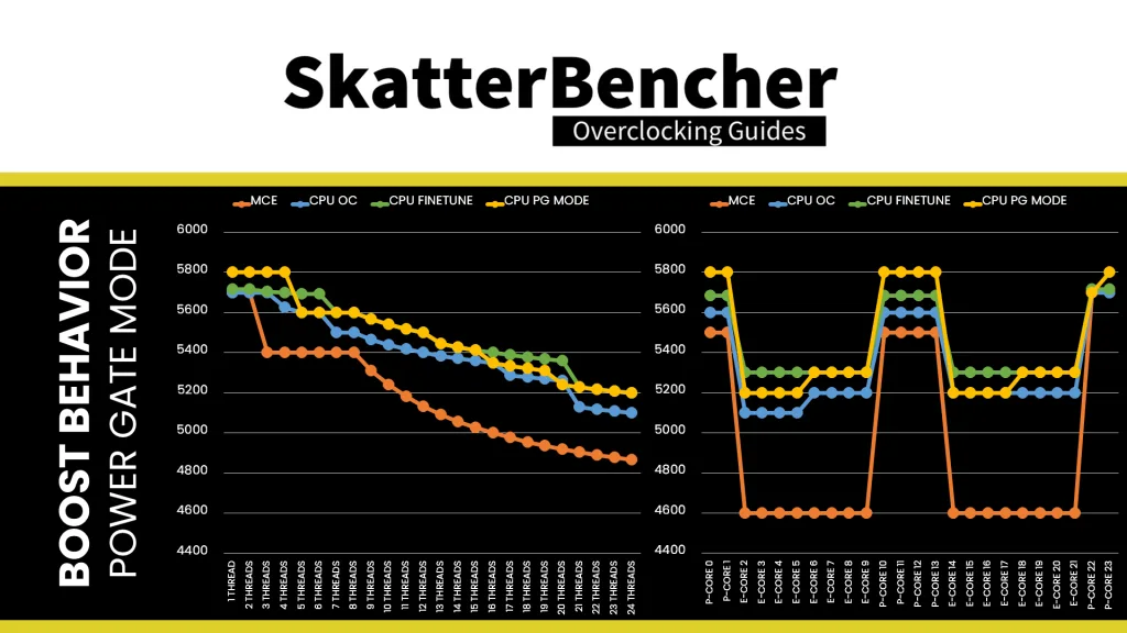
The crucial part of all-core tuning in PG mode is managing the output voltage with an appropriate VR load-line. The process to figure it out is pretty simply: set the Turbo Ratio Limit for all-core to the maximum Per Core Ratio Limit, then check stability. If unstable, increase the VR load-line. If you hit TjMax, reduce the VR load-line and/or reduce the Turbo Ratio Limit.
In my case, I opted for Level 6 CPU load-line. At a set voltage of 1.375V, that gives me about 1.25V in a heavy all-core workload.
Once you’ve defined the output voltage and the load-line, it’s a matter of finding the maximum stable CPU core ratio given the load-line slope. This is a bit trial and error as the P-cores and E-cores put different load on the VRM.
For example, at idle the voltage is 1.375V. With 1 active P-core, the load-line drops it to 1.34V. With 4 active P-cores, the voltage is 1.32V, and with all 8 P-cores active it’s 1.29V. On the contrary, 8 active E-cores only drops the voltage to 1.32V. And even 16 active E-cores don’t drop the voltage as low as having 8 P-cores active.
I found there was little difference in maximum nT frequency with DLVR mode, so I retained the same configuration: 56X for the P-cores and 50X for the E-cores.
BIOS Settings & Benchmark Results
Upon entering the BIOS
- Go to the Ai Tweaker menu
- Set Performance Preferences to ASUS Advanced OC Profile
- Set Ai Overclock Tuner to XMP I
- Set ASUS MultiCore Enhancement to Enabled – Remove All Limits
- Set Performance Core Ratio to By Core Usage
- Set 1-Core to 4-Core Ratio Limit to 58
- Set 5-Core and 8-Core Ratio Limit to 56
- Enter the Specific Performance Core submenu
- Set all Performance Core except Core 5 Specific Ratio Limit to 58.00
- Set Performance Core5 Specific Ratio Limit to 57.00
- Leave the Specific Performance Core submenu
- Set Efficient Core Ratio to By Core Usage
- Enter the By E-Core Usage submenu
- Set Efficient Turbo Ratio Limit 1 to 53
- Set Efficient Turbo Ratio Cores 1 to 4
- Set Efficient Turbo Ratio Limit 2 to 52
- Set Efficient Turbo Ratio Cores 2 to 8
- Set Efficient Turbo Ratio Limit 3 to 51
- Set Efficient Turbo Ratio Cores 3 to 12
- Set Efficient Turbo Ratio Limit 4 to 50
- Set Efficient Turbo Ratio Cores 4 to 16
- Leave the By E-Core Usage submenu
- Enter the Specific Efficient Core submenu
- Set Efficient Core Group0 and Group2 Specific Ratio Limit to 52
- Set Efficient Core Group1 and Group3 Specific Ratio Limit to 53
- Leave the Specific Efficient Core submenu
- Set DRAM Frequency to DDR5-8600
- Enter the DRAM Timing Control submenu
- Enter the Memory Presets submenu
- Load the Hynix 9000 1.55v 2x16GB ADIE profile
- Leave the Memory Presets submenu
- Set DRAM RAS# to RAS# Delay L to 16
- Set DRAM Refresh Interval to 32768
- Set DRAM Write Recovery Time to 66
- Set tRDWR_sg and tRDWR_dg to 24
- Enter the Memory Presets submenu
- Leave the DRAM Timing Control submenu
- Enter the DIGI+ VRM submenu
- Set CPU Load-line Calibration to Level 6
- Leave the DIGI+ VRM submenu
- Enter the Thermal Velocity Boost submenu
- Set Overclocking TVB to Enabled
- Set OC TVB Configuration Limit to Per P-core Group
- Set OC TVB Ratio Item Mode to Per Core Mode
- Set 1- to 4- and 7- to 8-Core Active to Enabled
- For 1- to 4-Core Active, set Temperature A to 50
- For 1- to 4-Core Active, set Negative Ratio A Offset to 1
- For 1- to 4-Core Active, set Temperature B to 70
- For 1- to 4-Core Active, set Negative Ratio B Offset to 1
- For 7- and 8-Core Active, set Temperature A to 80
- For 7- and 8-Core Active, set Negative Ratio A Offset to 1
- Set Overclocking TVB to Enabled
- Leave the Thermal Velocity Boost submenu
- Enter the Tweaker’s Paradise submenu
- Set High d2d cold boot workaround to Enabled
- Leave the Tweaker’s Paradise submenu
- Set Max. CPU Cache Ratio to 42
- Set NGU Ratio to 34
- Set CPU D2D Ratio to 38
- Set Actual VRM Core Input Voltage to Manual Mode
- Set CPU Core Voltage Override to 1.375
- Set CPU DLVR Mode to Power Gate Mode
- Set CPU System Agent Voltage to Manual Mode
- Set CPU System Agent Voltage Override to 1.300
- Set VNNAON 0.77v Voltage to Manual Mode
- Set VNNAON Voltage Override to 1.000
Then save and exit the BIOS.
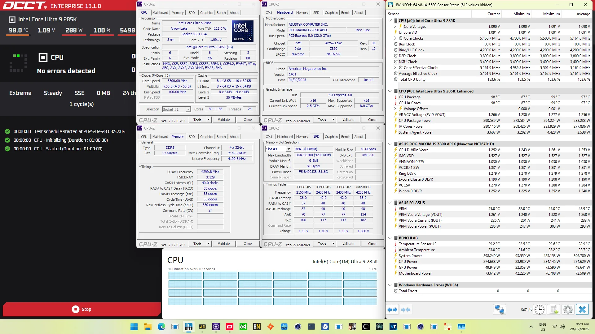
The CPU boost frequency with 1 active P-core is 5800 MHZ. The average boost frequency gradually trails off to 5600 MHz when all P-cores are active and to 5200 MHz when all P- and E-cores are active. In single-threaded applications, seven P-cores can boost to 5800 MHz while one can only boost to 5700 MHz. Two E-core clusters can boost to 5.3 GHz and the other two boost to 5.2 GHz.
We re-ran the benchmarks and checked the performance increase compared to the default operation.
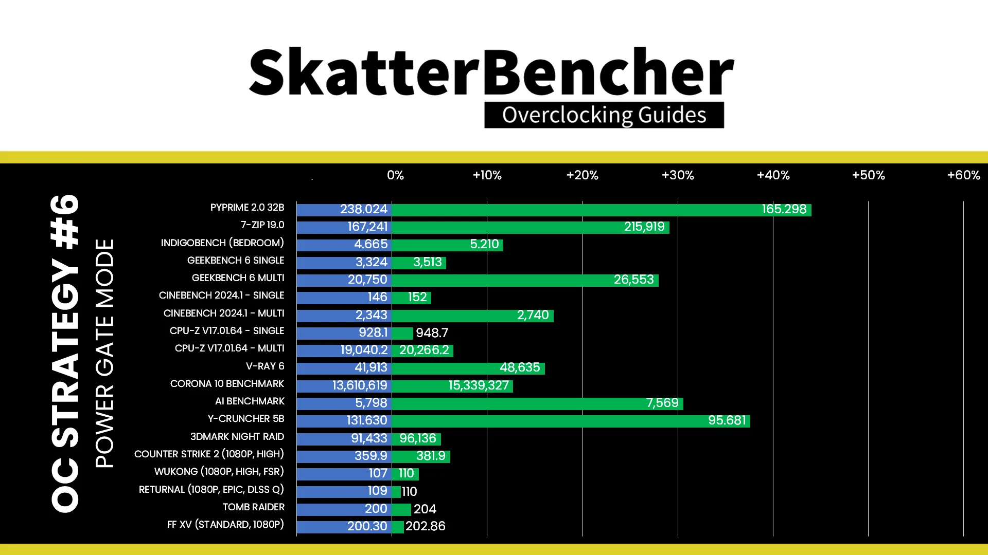
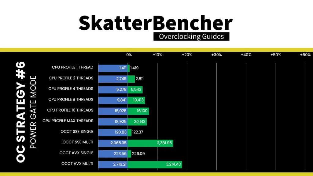
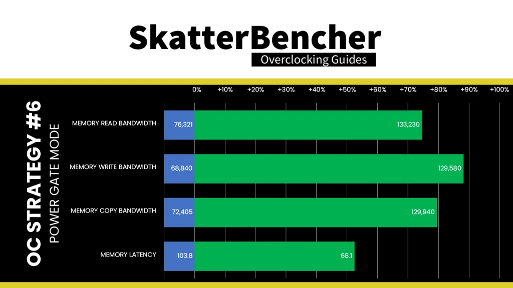
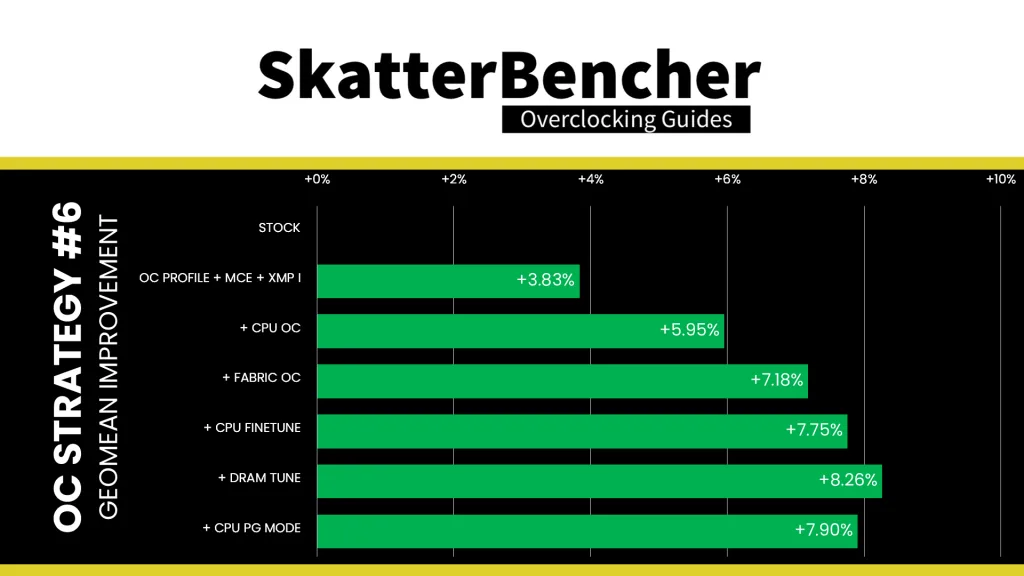
While Power Gate mode isn’t officially supported anymore, my experience proves it has a place in Intel’s overclocking toolkit for regular users, even if the strict voltage limits would be enforced. For example, in my case, I could quite easily get close to the performance for a maximum DLVR tune which took weeks to figure out. Our PG mode performance even beats the best DLVR configuration in some heavy all-core workloads like Y-Cruncher and AI Benchmark The Geomean performance regresses by 0.36 percentage points, and we get a maximum improvement of +44.00% in PyPrime.
When running the OCCT CPU AVX2 Stability Test, the average CPU P-core effective clock is 5482 MHz, and the average CPU E-core effective clock is 5000 MHz with 1.249 volts. The average CPU temperature is 104.0 degrees Celsius. The average CPU package power is 311.6 watts.
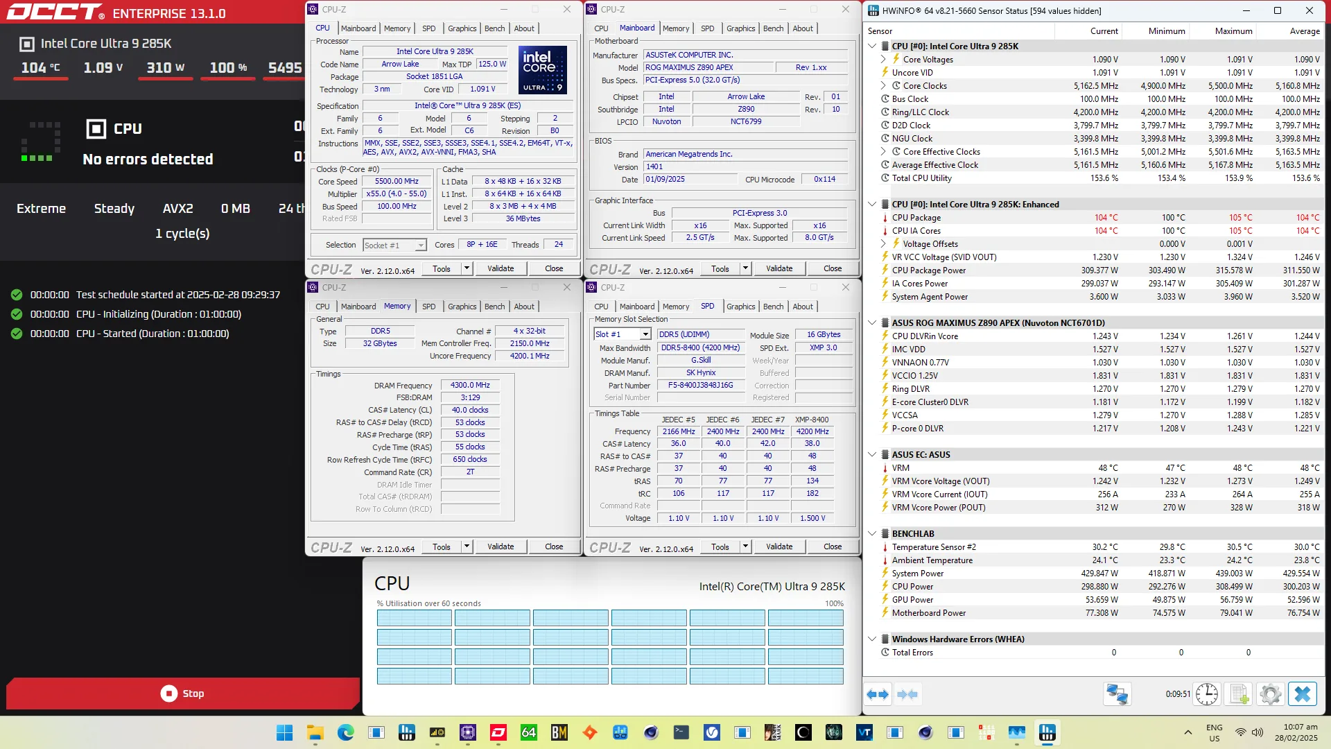
When running the OCCT CPU SSE Stability Test, the average CPU P-core effective clock is 5500 MHz, and the average CPU E-core effective clock is 5000 MHz with 1.260 volts. The average CPU temperature is 97.0 degrees Celsius. The average CPU package power is 288.2 watts.
Intel Core Ultra 9 285K: Conclusion
Let’s wrap this up.
The Core Ultra 9 285K is Intel’s top of the line Arrow Lake processor and it certainly feels they squeezed the chip for all it has. It’s one of the most difficult chips I’ve ever had the pleasure of tuning.
Especially overclocking the P-cores is like trying to squeeze blood out of a stone. It doesn’t seem to scale with voltage or have any headroom with the default curve. All that’s possible is getting the non-favored cores to run close to 5.7 GHz and lift the all-core frequency as high as possible.
The E-cores have a little bit more overclocking headroom, though we also see limited scaling with voltage. The positive thing is that the E-cores are quite powerful so increasing the frequency helps improve performance.
Tuning the memory subsystem is a lot more enjoyable and also translates into performance gains. There’s a lot of headroom for the NGU and the D2D, and Arrow Lake can hit high memory frequencies quite easily. The Ring is a different story as it’s the same as the P-cores: no voltage scaling and little to no headroom.
Anyway, that’s it for this video. I’m already working on the next Arrow Lake overclocking guide so subscribe if you’re interested in the Core Ultra 7 265K. Though I’ll be traveling for work the next couple of months, so don’t expect the video too soon.
I want to thank my Patreon supporters and YouTube members for supporting my work. If you have any questions or comments, please drop them in the comment section below.
See you next time!
Alex
Coul you help me to get a profile for that (mine) processor for Intel Extreme Tuning app?
Raul VLAD
Hi Pieter i’ve sent you a mail and a private message on fbk if you got some time to take a look on. Thanks
Pieter
Hi! I saw your email flash by but had a busy week so haven’t had the time to reply. Will try to get around it this weekend.
Reg
What’s the equivalent on Gigabyte Aorus boards (to that ASUS MCE) ?
Also, are the strategies supposed to be combined, or do I pick one over hte other? In other words, if I want to overclock my 285K, can i just start reading from the best-ranked strategy, or should i apply all strategies, one after another, to get that 8% boost ?
Thanks
Pieter
I’m not familiar with the GIGABYTE Z890 boards but I believe they do have an option that also unlocks all Turbo Boost limiters.
As for the strategies: they work independent. So you can pick one of the strategies and use the settings as a base for your overclock. The settings do build progressively across the strategies, so I take what I learned from OC Strategy #1 into Strategy #2. My suggestion would be to go step by step and see where the trade-off of time spent vs perf gained isn’t worth it for you anymore.
ArrowLakeUser
Thanks bro for the writeup, it explained very well about the new Arrow Lake tuning feature!
bigFan88
hey just want to say thank you for your great work! i know ARL-S has been a bit of a disappointment, but i think you’ll start to see some more volume with the recent intel gamer days BF6 promo. cheers to you!