SkatterBencher #93: Radeon Graphics (Ryzen 9000) Overclocked to 3000 MHz
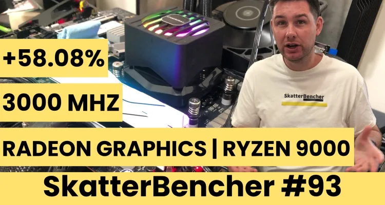
We overclock the AMD Radeon Graphics integrated in the Ryzen 9 9900X processor up to 3000 MHz with the ASUS ROG Crosshair X870E hero.
While I wouldn’t say overclocking the integrated graphics provides a viable path to meaningful performance, this wouldn’t be SkatterBencher if we didn’t try to squeeze performance anyway. And it turns out there’s much more to IGP tuning that you’d expect.
In this guide, I break down the Radeon Graphics tuning process into four unique overclocking strategies for beginner and advanced overclockers.
- First, we enable Precision Boost Overdrive 2 and EXPO,
- Second, we overclock the graphics core,
- Third, we tune the memory subsystem performance,
- And, finally, we mess around with Graphics Curve Optimizer.
However, before we jump into overclocking, let us quickly review the hardware and benchmarks used in this guide.
AMD Radeon Graphics (Granite Ridge): Introduction
The AMD Radeon Graphics integrated in the Ryzen 9000 series CPUs is identical to the one from the Ryzen 7000 CPUs. In fact, we overclocked Radeon Graphics before in SkatterBencher #55.
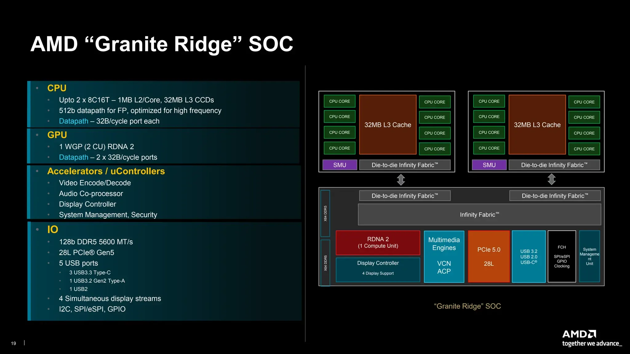
The IGP features the somewhat outdated RDNA 2.0 architecture in its smallest form: we get exactly 1 WGP (WorkGroup Processor). The WGP is the basic unit of compute. In RDNA 2.0, one WGP encompasses 2 CUs (Compute Units) as well as 2 ray-tracing accelerators.
To give you an idea of how little compute that is: the AMD Radeon RX 6500 XT we overclocked in SkatterBencher #41 has 8 WGP; and that is the lowest-end RDNA 2 discrete graphics card you could buy in retail!
Just like in the Ryzen 7000 CPUs, the Radeon Graphics for Ryzen 9000 is clocked at 2.2 GHz out of the box.
Platform Overview
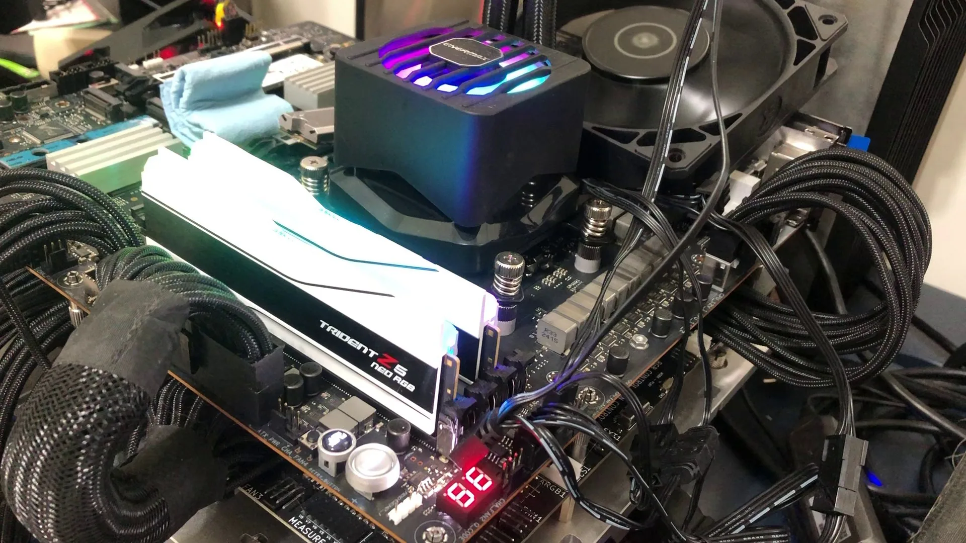
The system we’re overclocking today consists of the following hardware.
| Item | SKU |
|---|---|
| CPU | AMD Ryzen 9 9900X |
| Motherboard | ASUS ROG Crosshair X870E Hero |
| CPU Cooling | Enermax LIQMAXFLO 420 |
| Memory | G.SKILL Trident Z5 Neo DDR5-8000 32GB |
| Graphics Card | GALAX GeForce RTX 4090 HOF |
| Storage | AORUS RGB NVMe M.2 512GB Gen4 AGI 512GB NVMe M.2 Gen3 |
| Chassis | Open Benchtable V2 |
| Telemetry | BENCHLAB |
Benchmarks, Games & Tools
We use Windows 11 and the following benchmark applications and games to measure performance and ensure system stability.
| Benchmark | Link |
|---|---|
| Geekbench 6 | https://www.geekbench.com/ |
| Geekbench AI | https://www.geekbench.com/ai/ |
| Novabench | https://novabench.com/ |
| AI-Benchmark | https://ai-benchmark.com/ |
| MLPerf Client 1.0 | https://mlcommons.org/benchmarks/client/ |
| Furmark 2.9 | https://geeks3d.com/furmark/ |
| GravityMark | https://gravitymark.tellusim.com/ |
| 3DMark FSR Feature Test | https://www.3dmark.com/ |
| Superposition | https://benchmark.unigine.com/superposition |
| Spaceship | https://store.steampowered.com/app/1605230/Spaceship__Visual_Effect_Graph_Demo/ |
| Evolve | https://store.steampowered.com/app/2717790/Evolve_Benchmark/ |
| AIDA64 | https://www.aida64.com/ |
| Memtest Vulkan | https://github.com/GpuZelenograd/memtest_vulkan |
| Game | Link |
|---|---|
| Counter Strike 2 | https://store.steampowered.com/app/730/CounterStrike_2/ |
| Returnal | https://store.steampowered.com/app/1649240/Returnal/ |
| Shadow of the Tomb Raider | https://store.steampowered.com/app/750920/Shadow_of_the_Tomb_Raider_Definitive_Edition/ |
| Monster Hunter Wilds | https://www.monsterhunter.com/wilds/en-us/benchmark/ |
| Age of Mythology Retold | https://store.steampowered.com/app/1934680/Age_of_Mythology_Retold/ |
| Forza Motorsport | https://store.steampowered.com/app/2440510/Forza_Motorsport/ |
| Homeworld 3 | https://store.steampowered.com/app/1840080/Homeworld_3/ |
I use the following tools to check and log system telemetry, adjust clock frequencies, and launch benchmarks.
AMD Radeon Graphics (Granite Ridge): Stock Performance
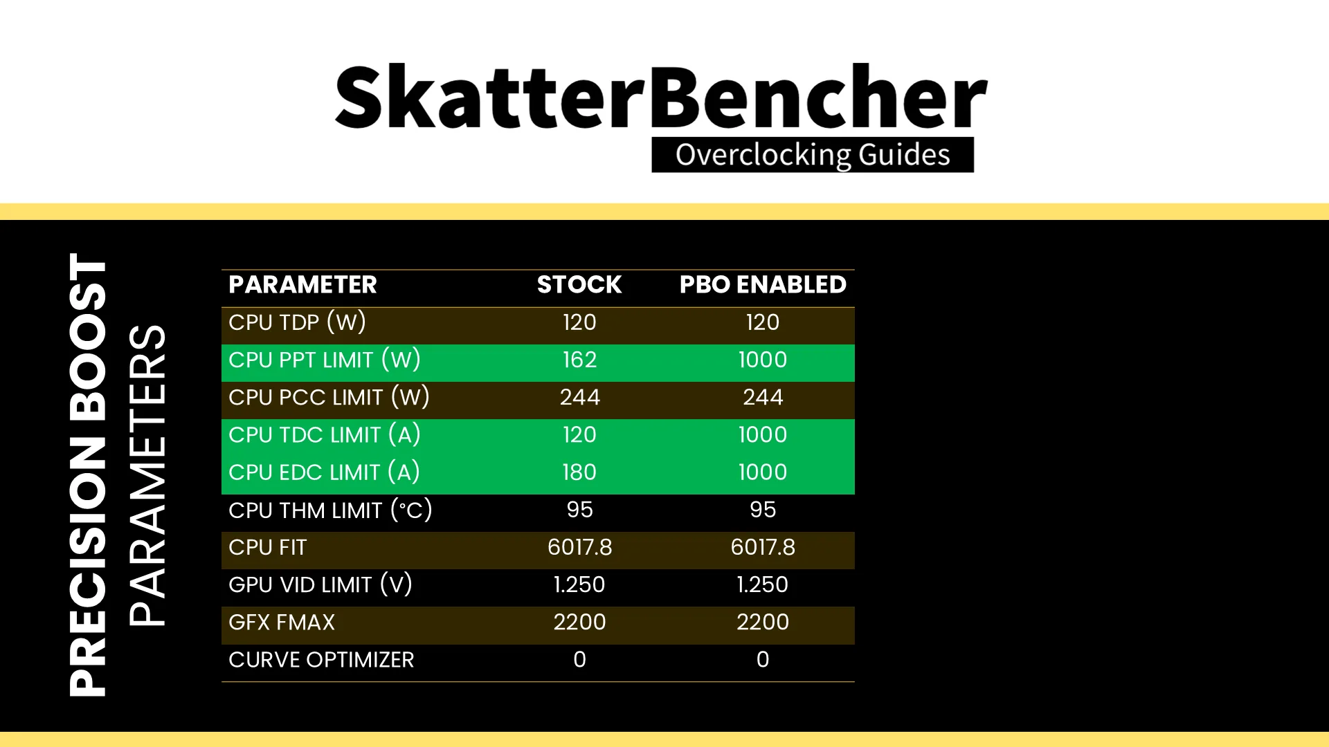
Before starting overclocking, we must check the system performance at default settings. The default Precision Boost 2 parameters for the Ryzen 9 9900X and its Radeon Graphics are as follows:
- PPT: 162 W
- TDP: 120 W
- PCC: 244 W
- TDC CPU: 120 A
- EDC CPU: 180 A
- THM: 95 C
- VID: 1.25 V
- GFX FMAX: 2200 MHz
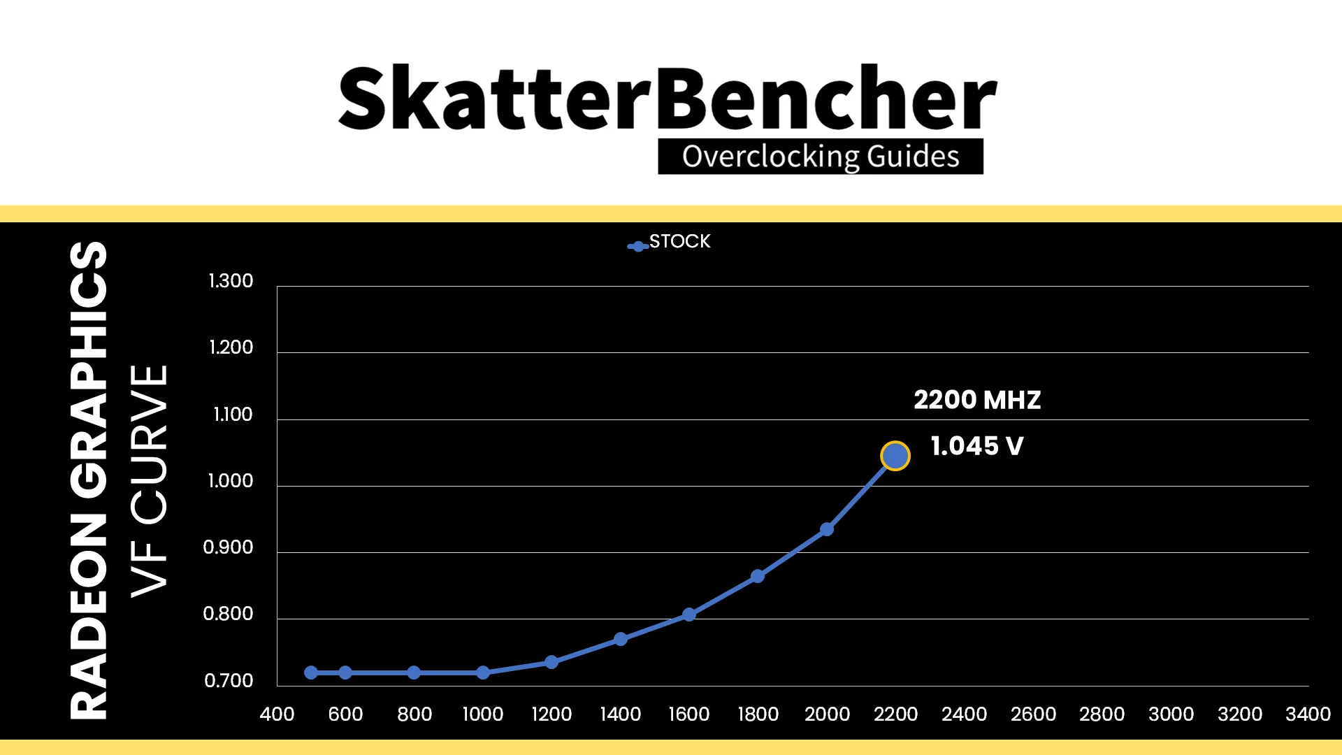
The Radeon Graphics has its own V/F curve, operating up to 2.2 GHz at 1.045V.
Since this guide focuses on IGP performance, I set the UMA Frame Buffer to 16 GB which is half of the total available system memory. UMA is an acronym for Unified Memory Architecture which is a technology that allows the processor and integrated graphics to share the memory.
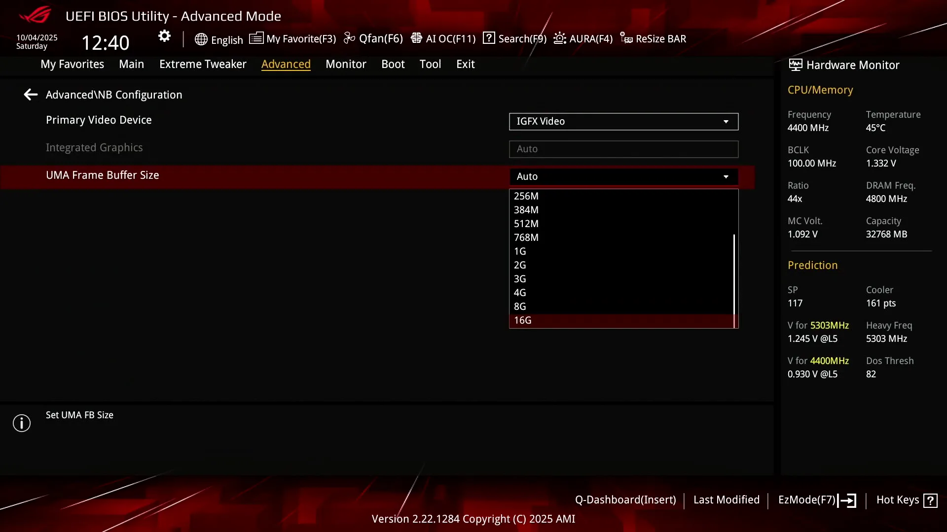
The UMA Frame Buffer is the portion of the system memory that’s exclusively reserved for the integrated graphics. The rest of the system memory can be accessed by both IP. Usually, you don’t need to adjust the UMA Frame Buffer but it can help for certain applications.
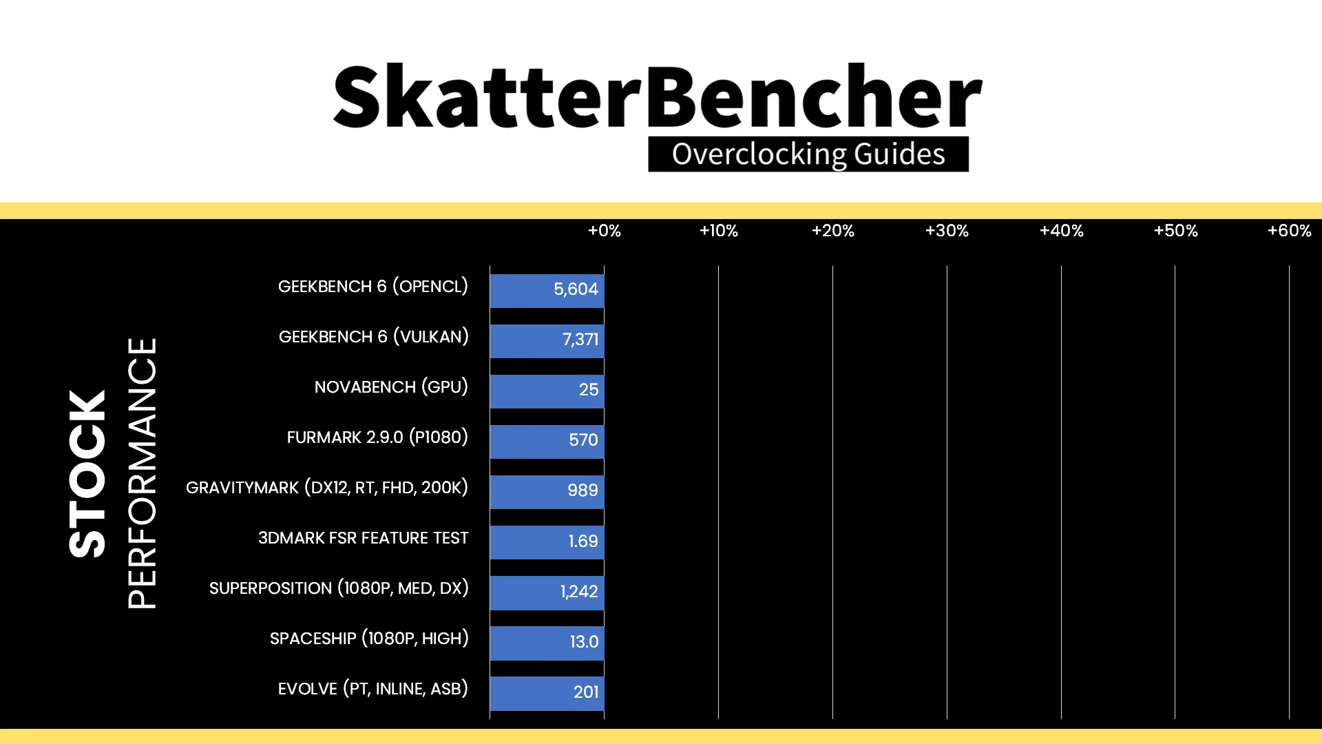
Here is the benchmark performance at stock:
- Geekbench 6 (OPENCL): 5,604 pts
- Geekbench 6 (VULKAN): 7,371 pts
- Novabench (GPU): 25 pts
- Furmark 2.9.0 (P1080): 570 pts
- GravityMark (DX12, RT, FHD, 200K): 989 pts
- 3DMark FSR Feature Test: 1.69 pts
- Superposition (1080P, MED, DX): 1,242 pts
- Spaceship (1080P, HIGH): 13.0 fps
- Evolve (PT, INLINE, ASB): 201 pts
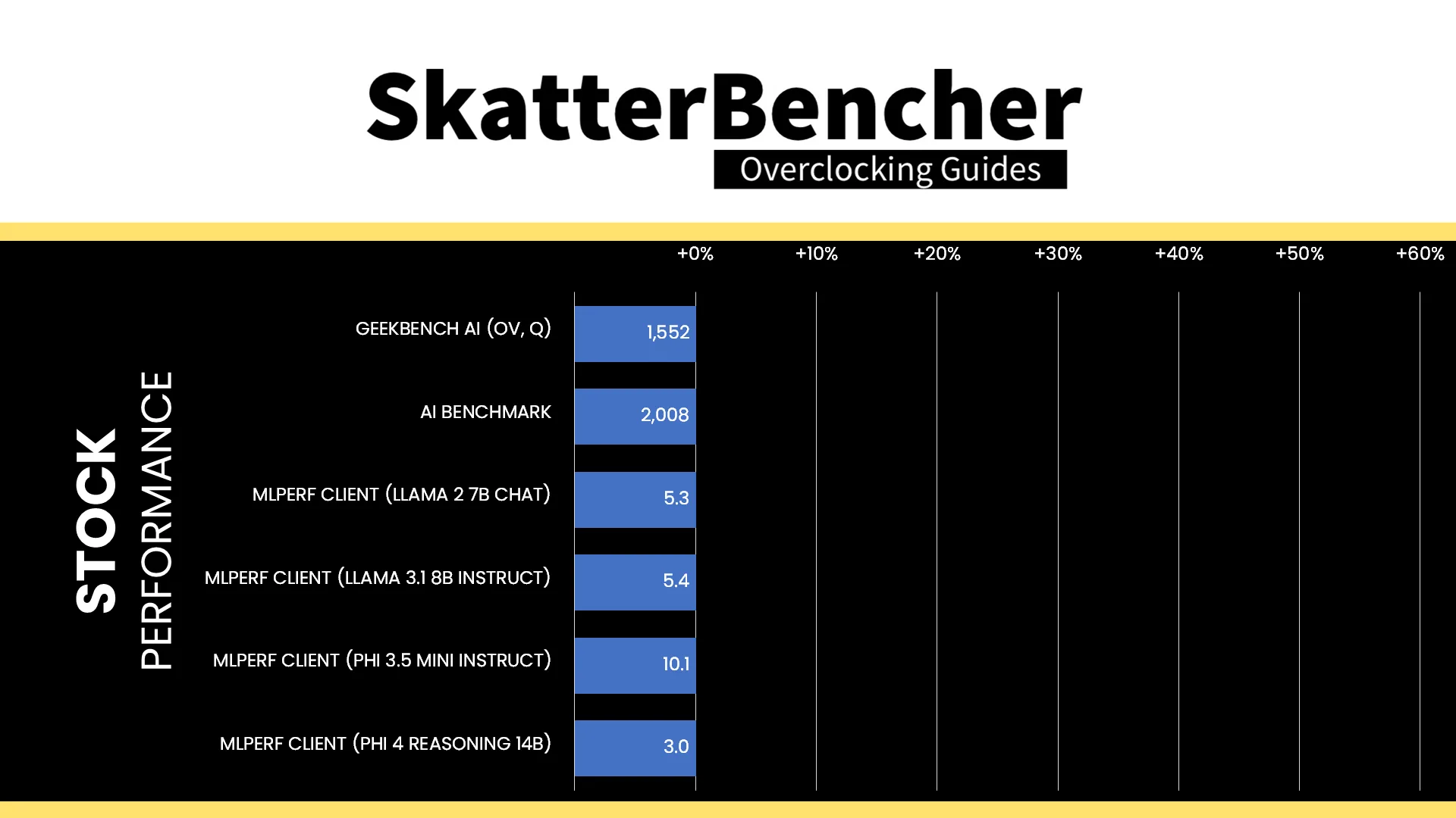
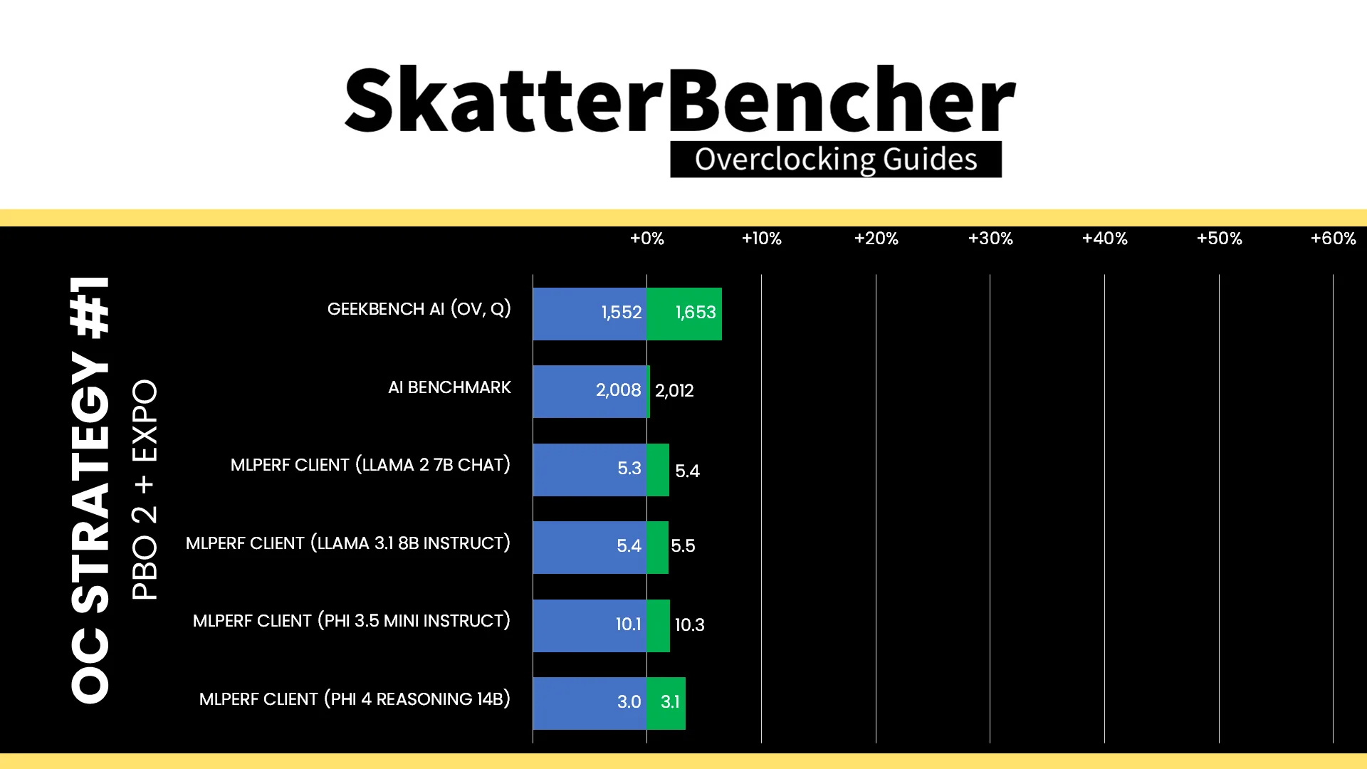
Here is the AI performance at stock:
- Geekbench AI (OV, Q): 1,552 pts
- AI Benchmark: 2,008 pts
- MLPerf Client (Llama 2 7B Chat): 5.3 tokes / sec
- MLPerf Client (Llama 3.1 8B Instruct): 5.4 tokes / sec
- MLPerf Client (Phi 3.5 MINI Instruct): 10.1 tokes / sec
- MLPerf Client (Phi 4 Reasoning 14B): 3.0 tokes / sec
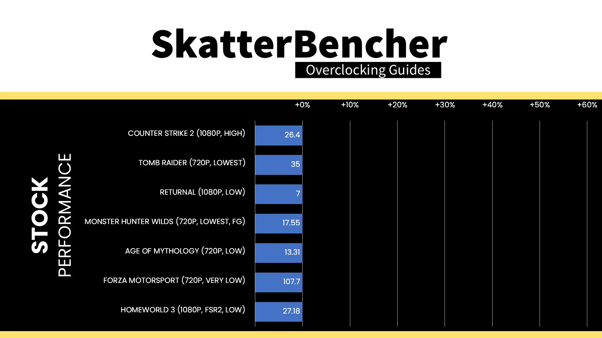
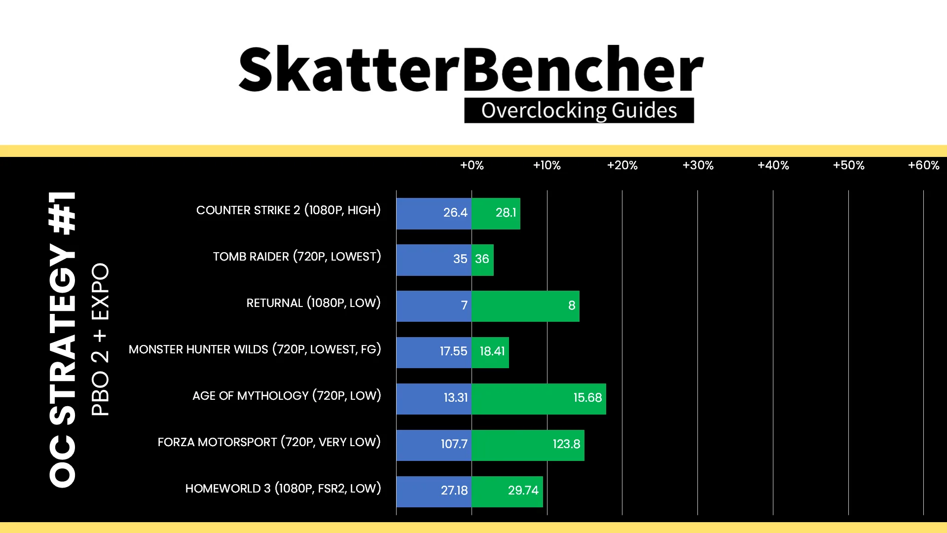
Here is the game performance at stock:
- Counter Strike 2 (1080P, HIGH): 26.4 fps
- Tomb Raider (720P, LOWEST): 35 fps
- Returnal (1080P, LOW): 7 fps
- Monster Hunter Wilds (720P, LOWEST, FG): 17.55 fps
- Age of Mythology (720P, LOW): 13.31 fps
- Forza Motorsport (720P, VERY LOW): 107.7 fps
- Homeworld 3 (1080P, FSR2, LOW): 27.18 fps
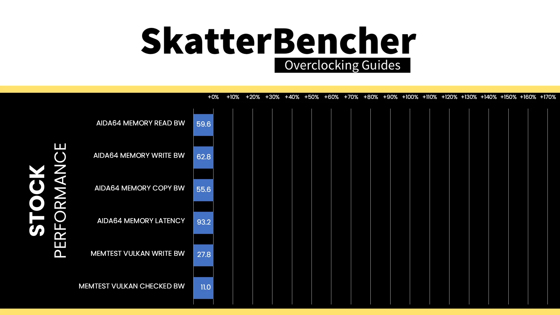
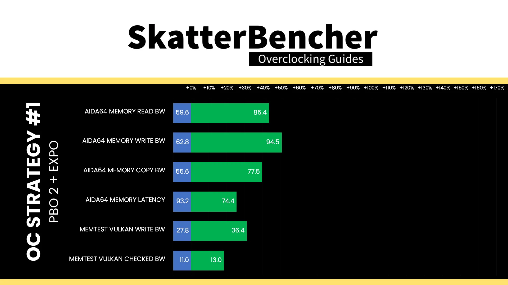
Here is the memory performance at stock:
- AIDA64 Memory Read Bandwidth: 59,583 MB/sec
- AIDA64 Memory Write Bandwidth: 62,830 MB/sec
- AIDA64 Memory Copy Bandwidth: 55,578 MB/sec
- AIDA64 Memory Latency: 93.2 ns
- Memtest Vulkan Write: 27.8 GB/sec
- Memtest Vulkan Checked: 11.0 GB/sec
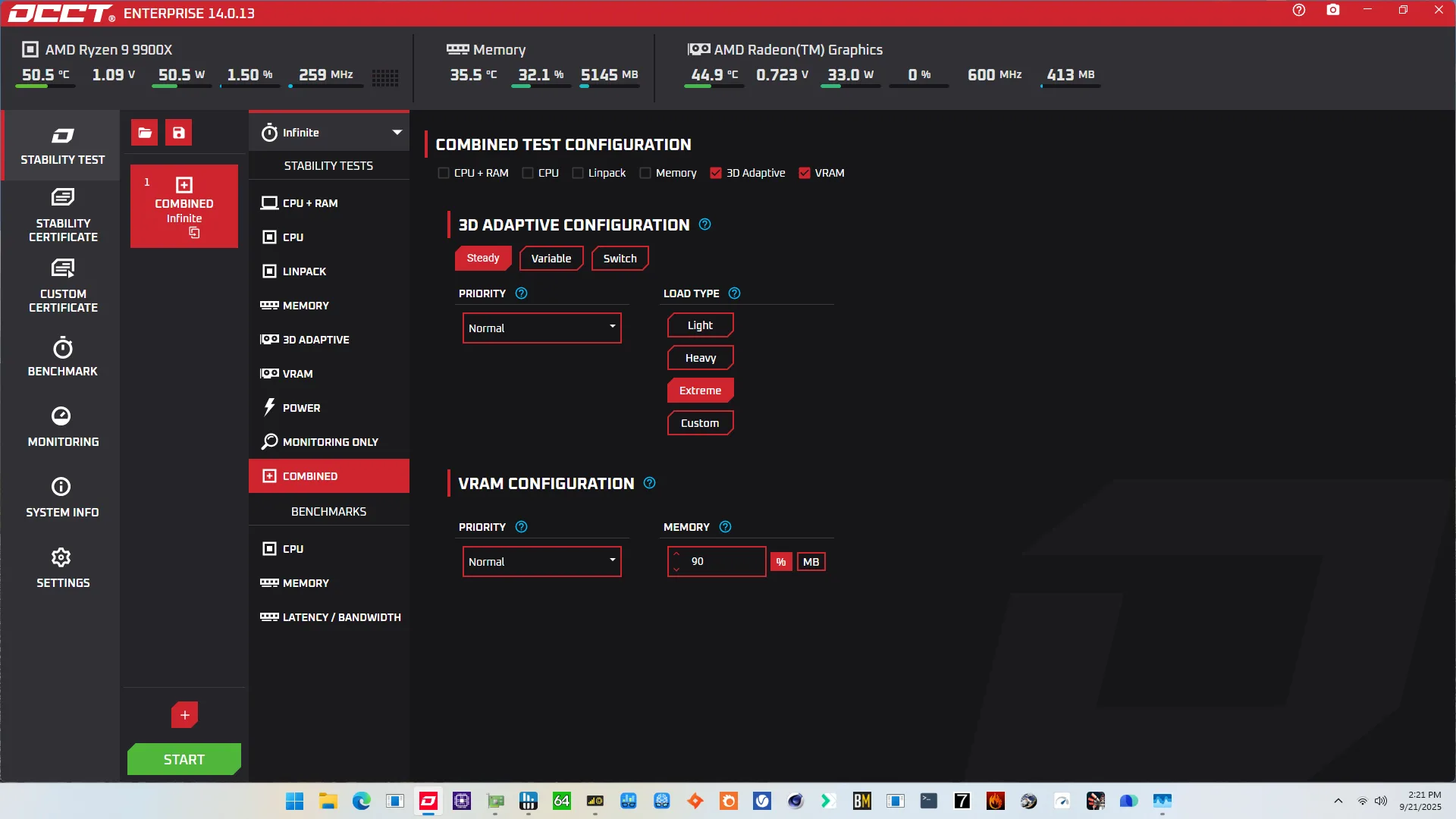
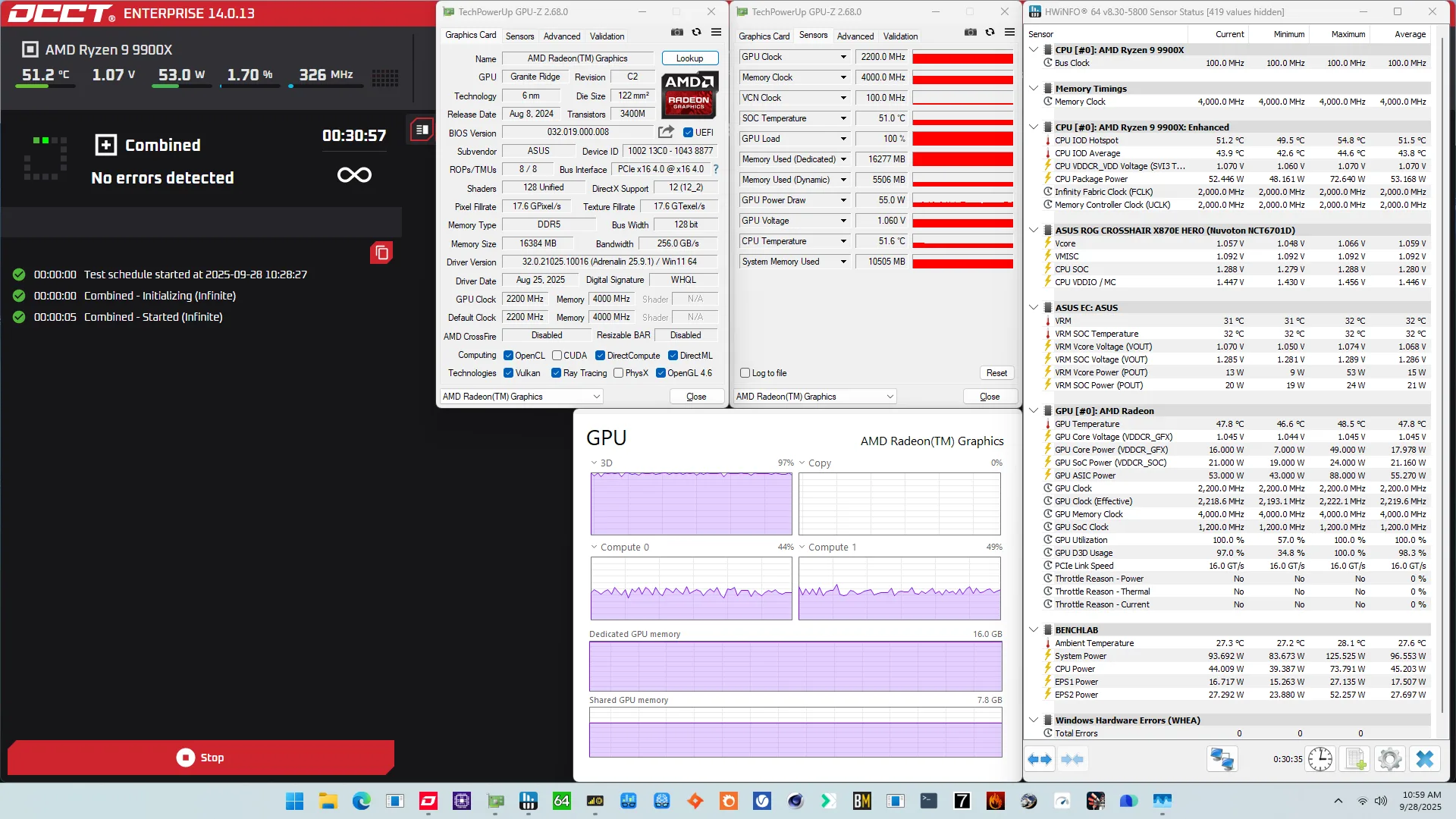
For the stress test part of the guide, I still rely on OCCT (as I usually do) but rather than picking one specific workload, I used its combination function to run both 3D Adaptive and VRAM workload at the same time. The reason is simple: I want to stress test the GPU and dedicated portion of the DDR5 memory at the same time.
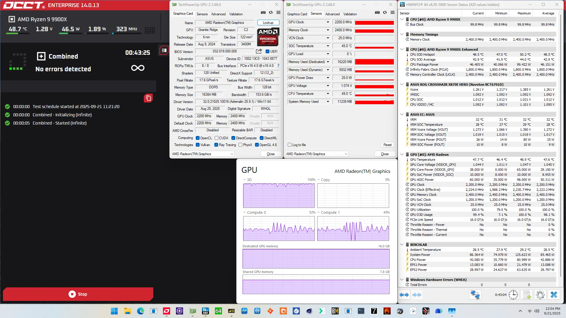
When running the OCCT 3D Adaptive and VRAM Combined Stress Test , the average GPU effective clock is 2223 MHz with 1.272 volts. The average GPU temperature is 47.6 degrees Celsius. The average GPU core power is 29.2 watts.
Of course, we can increase the maximum power consumption limit using Precision Boost Overdrive. That’s what we’ll do in our first overclocking strategy.
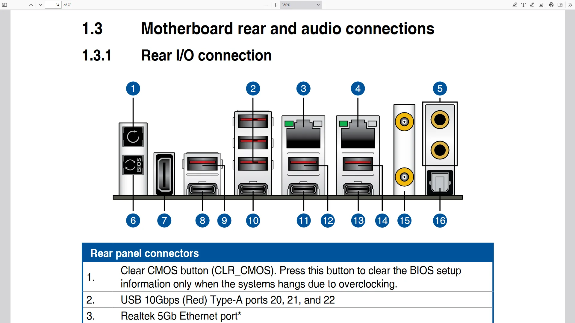
However, before we get going, make sure to locate the CMOS Clear button. Pressing the Clear CMOS button will reset all your BIOS settings to default, which is helpful if you want to start your BIOS configuration from scratch. The Clear CMOS button is located on the back I/O of the motherboard.
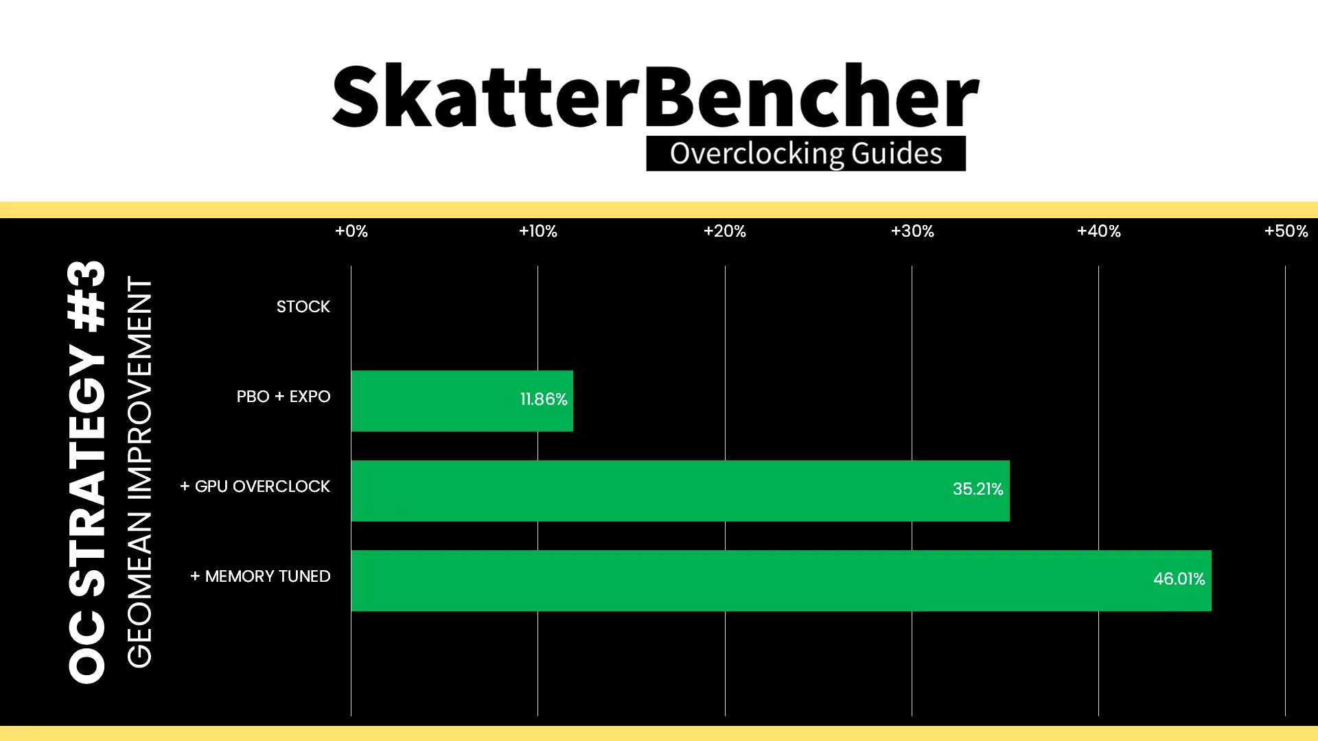
OC Strategy #1: PBO + EXPO
In our first overclocking strategy, we simply take advantage of enabling AMD Precision Boost Overdrive 2 and AMD EXPO.
Precision Boost Overdrive 2
Similar to the CPU cores, the performance of the integrated Radeon Graphics is subject to Precision Boost 2 governance. In other words, the Precision Boost performance limiters can also constrain graphics performance. Some performance limits are shared between CPU cores and the graphics, but some are IP block specific.
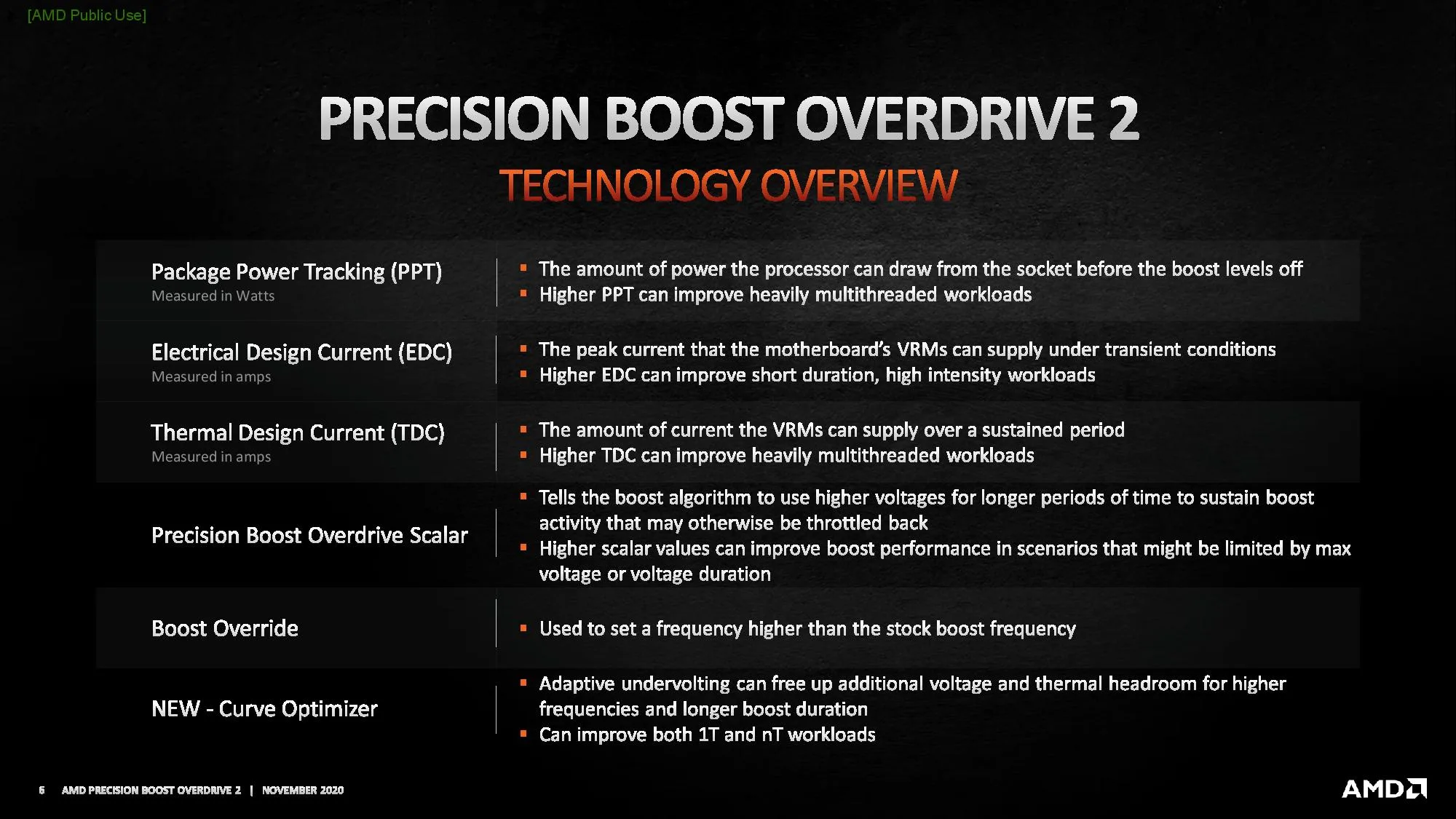
The Precision Boost Overdrive 2 toolkit for Radeon Graphics includes the overclocking knobs from Zen+ (PPT, TDC, EDC) and Zen 3 (Curve Optimizer). Unfortunately, there’s no GFX Fmax Boost Override like we have on Ryzen 8000G APUs.
There are essentially 3 levels of Precision Boost Overdrive
- AMD’s stock values, which can be set by disabling PBO
- The motherboard vendor values, which are programmed into BIOS to match the motherboard VRM specification and can be set by enabling PBO
- Custom values, which can be programmed by the end-user
In this overclocking strategy, we’re just enabling Precision Boost Overdrive, whereas, in the following strategies, we’ll explore tuning the parameters. By enabling Precision Boost Overdrive, we rely on the motherboard pre-programmed PBO parameters. We find that the following values have changed:
Since the integrated graphics use very little power, we don’t expect enabling PBO to have a major impact on system performance.
EXPO – Extended Profiles for Overclocking
EXPO stands for AMD Extended Profiles for Overclocking. It is an AMD technology that enables ubiquitous memory overclocking for AMD platforms supporting DDR5 memory.
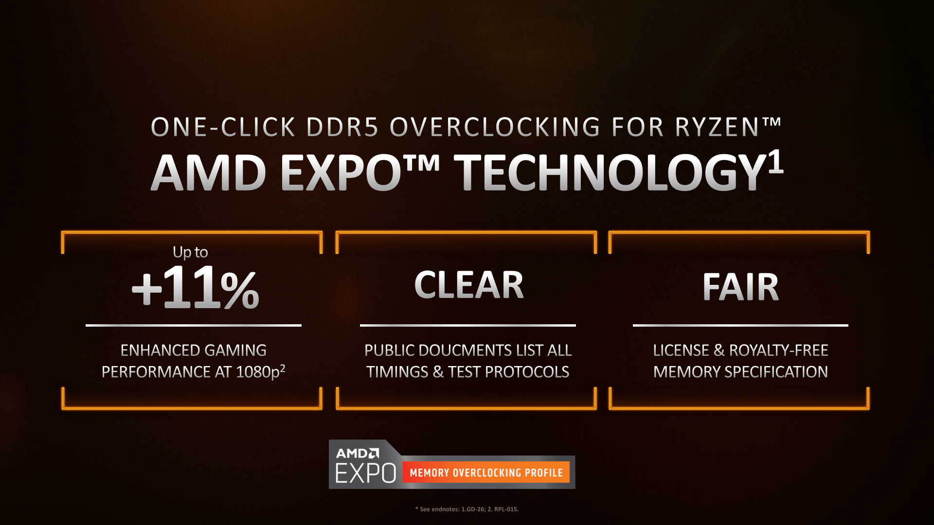
EXPO allows memory vendors such as G.SKILL to program higher performance settings onto the memory sticks. If the motherboard supports EXPO, you can enable higher performance with a single BIOS setting. So, it saves you lots of manual configuration.
Note that unlike in some other SkatterBencher guides, I could simply set EXPO I and run the memory kit at the EXPO-rated DDR5-8000.
BIOS Settings & Benchmark Results
Upon entering the BIOS
- Go to the Extreme Tweaker menu
- Set Ai Overclock Tuner to EXPO I
- Enter the Precision Boost Overdrive submenu
- Set Precision Boost Overdrive to enabled
- Switch to the Advanced menu
- Enter the NB Configuration submenu
- Set Primary Video Device to IGFX Video
- Set UMA Frame Buffer Size to 16G
Then save and exit the BIOS.
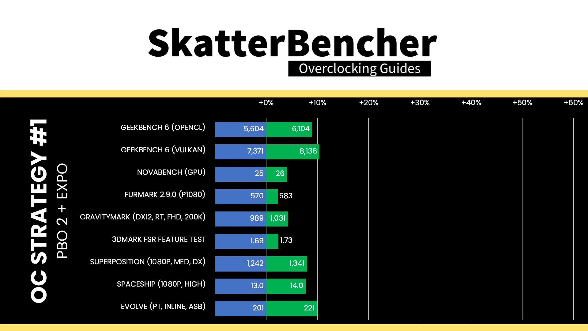
We re-ran the benchmarks and checked the performance increase compared to the default operation.
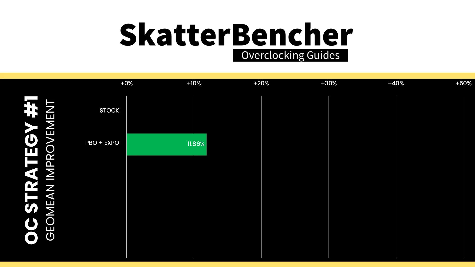
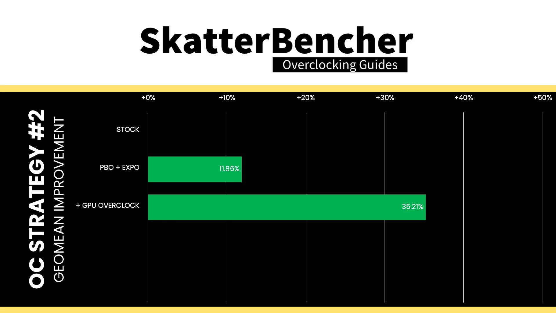
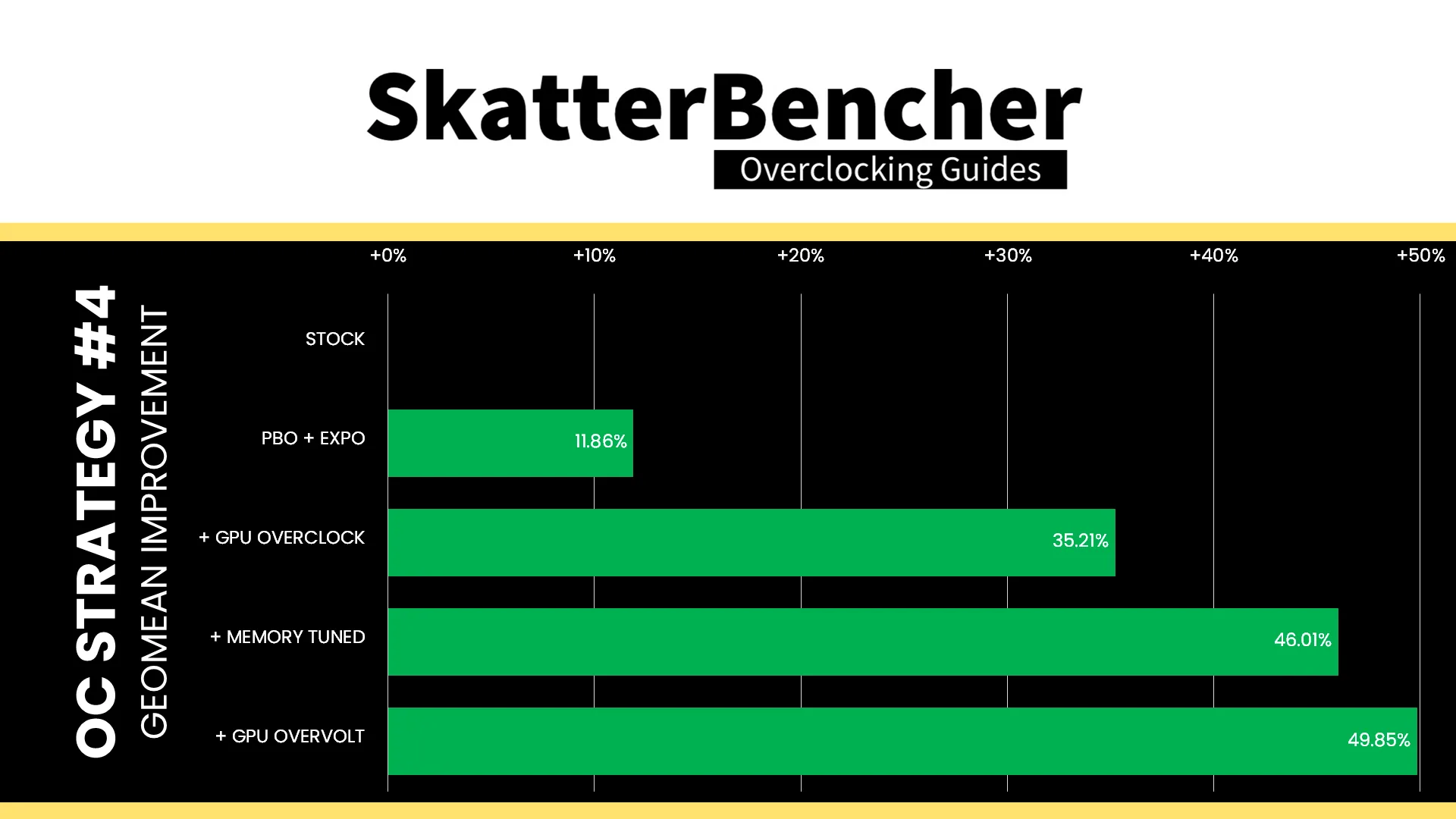
Enabling higher power limits doesn’t really affect Radeon Graphics since it operates well below the Precision Boost 2 performance limits. But, as we often see with integrated graphics, enabling higher memory performance makes a big impact on benchmark performance. The Geomean performance speedup is +11.86%, and we get a maximum benchmark speedup of +17.85% in Age of Mythology.
When running the OCCT 3D Adaptive and VRAM Combined Stress Test , the average GPU effective clock is 2221 MHz with 1.279 volts. The average GPU temperature is 50.5 degrees Celsius. The average GPU core power is 34.6 watts.

Higher Than Expected Graphics Voltage?
Attentive viewers will have raised their eyebrows twice by now because of the reported operating voltage in the OCCT stress tests. Both at stock and in OC Strategy #2, I state that the operating voltage is over 1.27 volt. However, the Radeon Graphics V/F curve clearly shows that 2.2 GHz should run at about 1.05 V.
So why do I say 1.27V? It’s because of the Granite Ridge voltage topology.
AMD Radeon Graphics (Granite Ridge): Voltage Topology
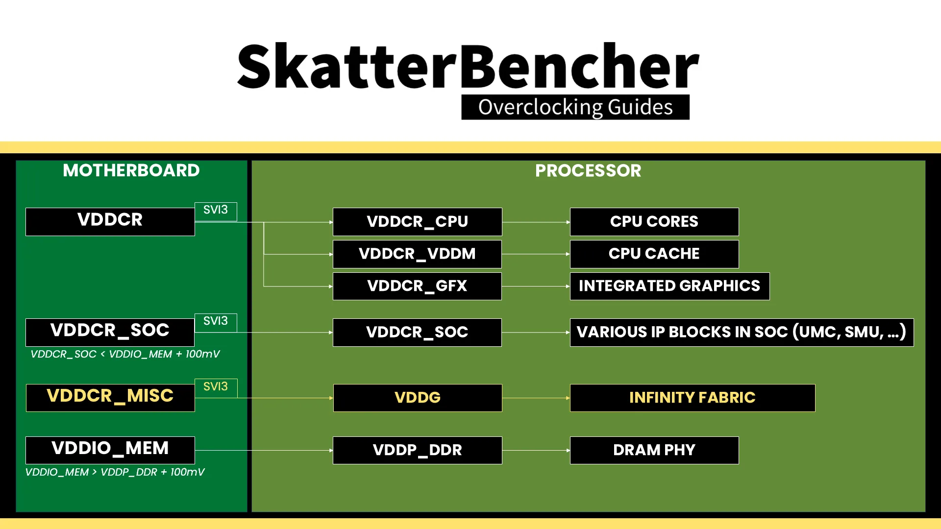
The Ryzen 9000 voltage topology relies on a combination of internal and external power supply to generate the processor voltages.
There are four primary power supplies from the motherboard VRM to the processor: VDDCR, VDDCR_SOC, VDDCR_MISC, and VDDIO_MEM_S3. Even though the integrated graphics IP block is located on the IO die with the rest of the SOC IP, it’s not powered by the VDDCR_SOC voltage rail but instead gets its power from the VDDCR voltage rail.
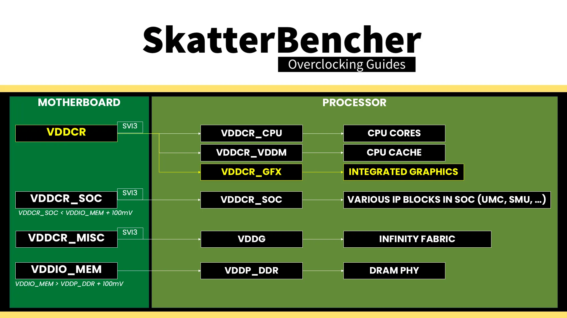
The VDDCR voltage rail provides external power for three internal voltage regulators: VDDCR_CPU, VDDCR_VDDM, and VDDCR_GFX.
- VDDCR_CPU provides the voltage for the CPU cores in CCX. The voltage rail can work in either dldo or bypass mode, but on Granite Ridge, it is always in bypass mode. That means the voltage is always equal to the VDDCR external voltage.
- VDDCR_VDDM provides the voltage for the L2, L3, and, if present, 3D V-Cache on a CCX. This rail cannot work in bypass mode; therefore, it is internally regulated from the VDDCR external voltage rail. The default VDDM voltage is 0.95V
- VDDCR_GFX provides the voltage for the integrated graphics. The voltage rail can work in either dldo or bypass mode, but on Granite Ridge, it is always in bypass mode. Crucially, that means the voltage is always equal to the VDDCR external voltage
The VDDCR voltage rail is directly controlled by the CPU SMU using an SVI3 interface. The voltage selected is the highest among the requests of its dependents. In this case, that’s the twelve CPU cores and the integrated graphics.
And that’s why the integrated graphics get more voltage than needed: it’s the CPU cores requesting the higher voltage from the VDDCR voltage rail! Of course, it would be better had the VDDCR_GFX rail had an option to enable dldo mode. Or, even better, if Radeon Graphics had their own voltage rail entirely like we often see on Intel platforms.
Impact on Power Consumption
The next question is how much the forced elevated voltage impacts power consumption. The easy way to check this is by setting a negative frequency boost override for the CPU cores. This ensures the highest voltage requested by the cores will be much lower.
I ran the same OCCT Combined Stress Test as OC Strategy #1 but with -1000 Fmax for the CPU cores. That results in 200mV lower operating voltage (1.06V vs 1.27V), almost 3 degrees Celsius lower operating temperature (47.8°C vs 50.5°C), and almost half the GPU Core Power usage (18.0W vs 34.6W).
While this tells us a more genuine story about the true GPU operating conditions, typically one wouldn’t downclock the CPU to get lower IGP power consumption. So, for the rest of the overclocking guide I’ll stick with the default CPU frequency.
OC Strategy #2: GPU Overclock
In our second overclocking strategy, we overclock the integrated graphics by setting GPU frequency as high as possible with the available BIOS options. But before we get into that, let’s have a closer look at the clocking topology.
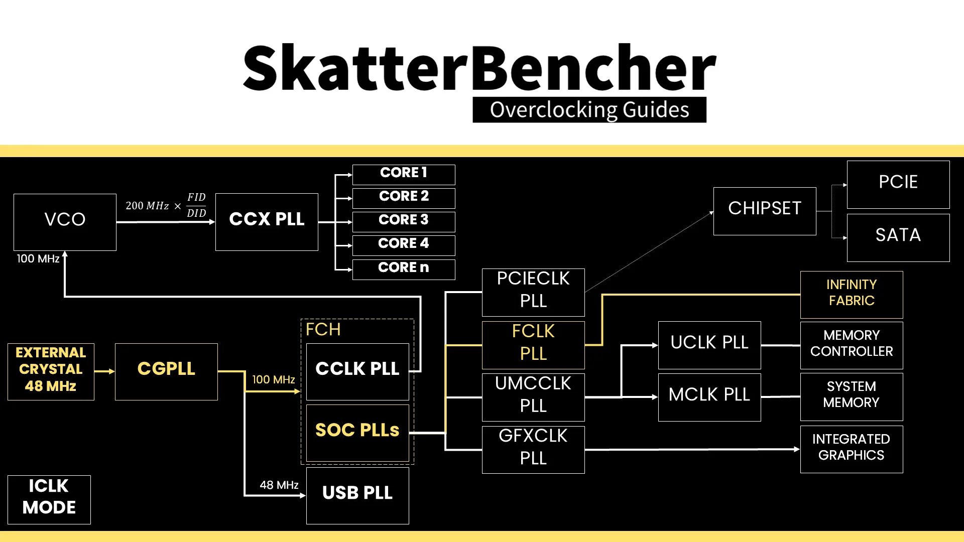
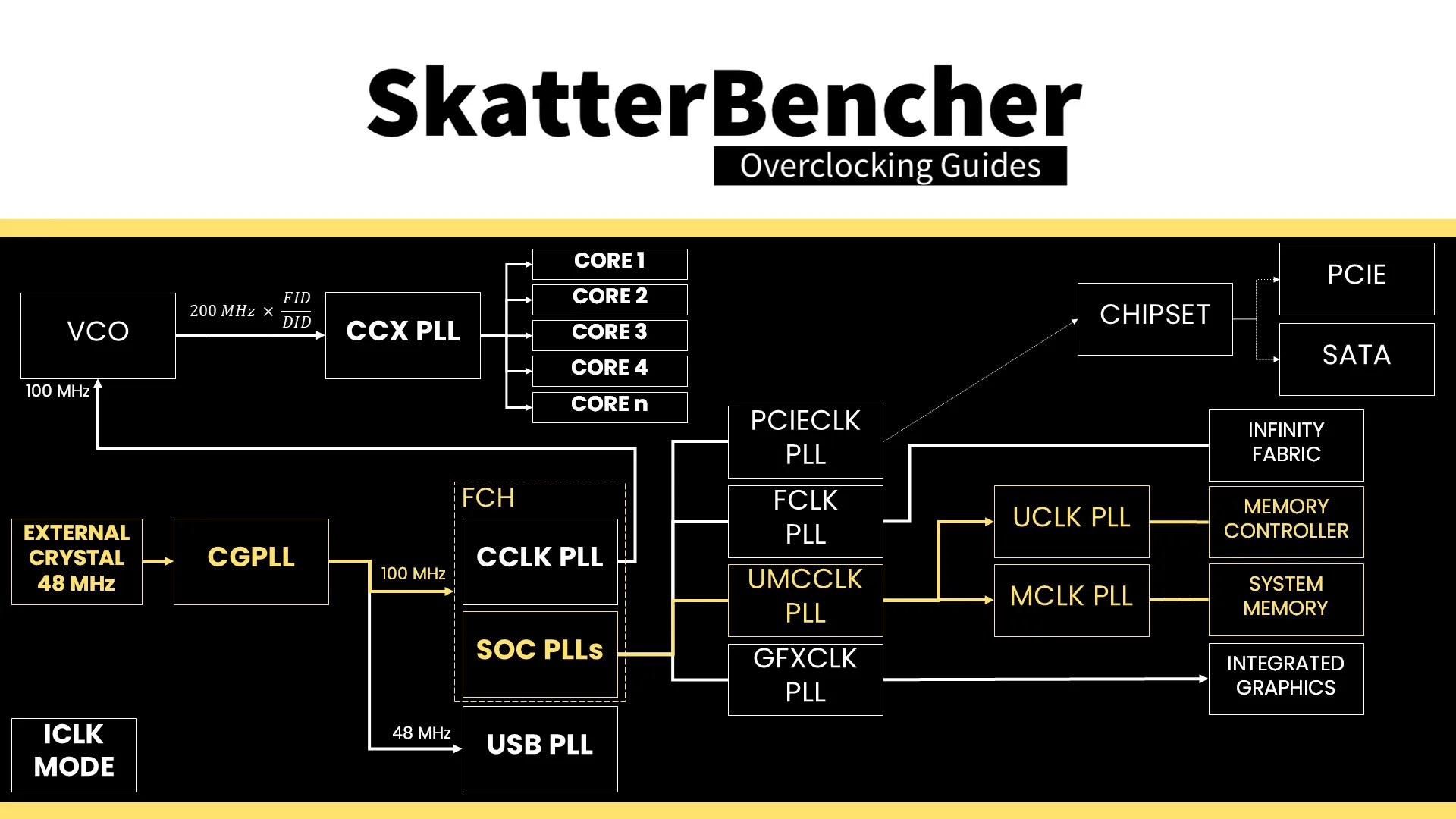
AMD Radeon Graphics (Granite Ridge): Clocking Topology
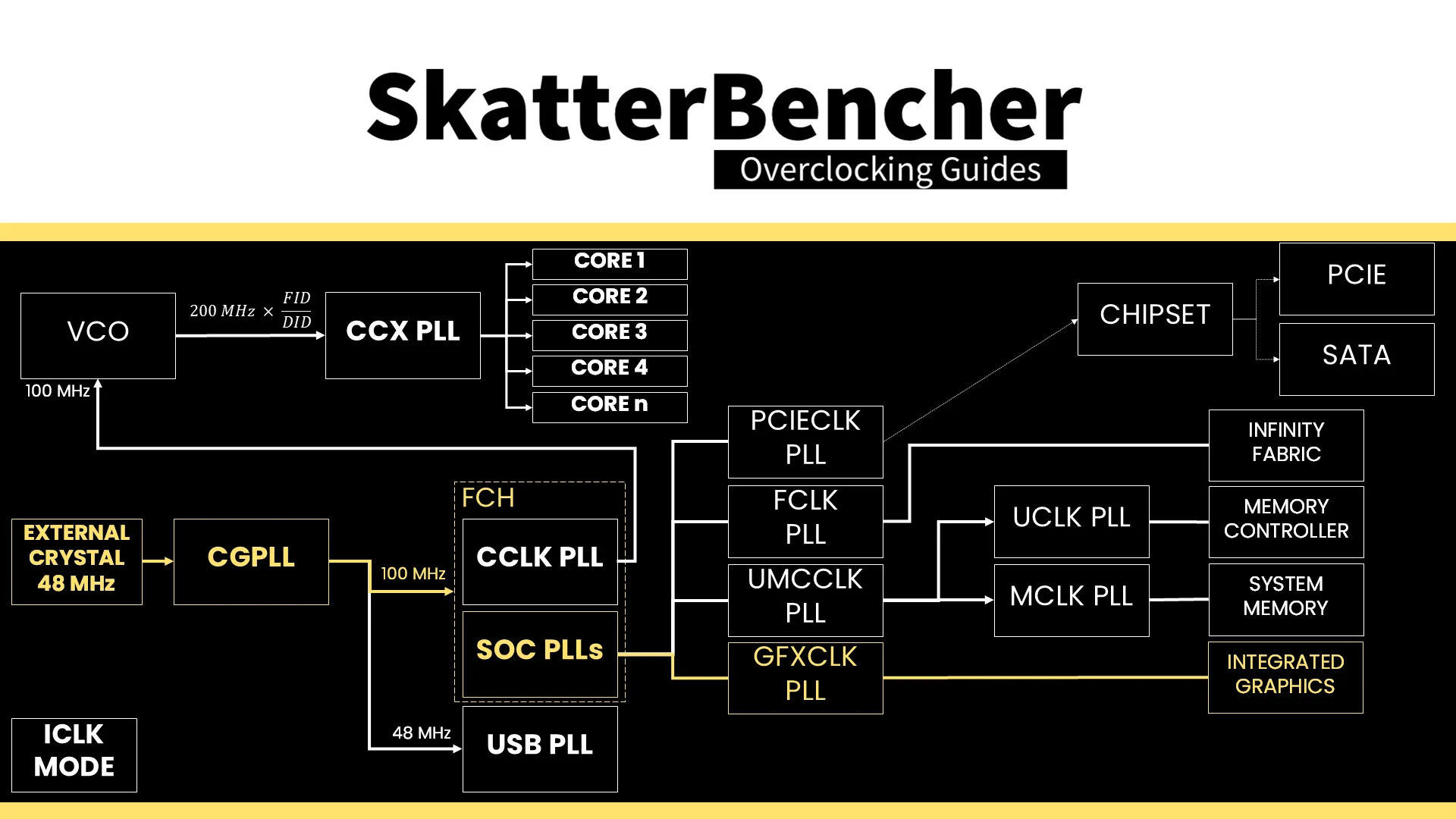
The Graphics frequency, or GFXCLK, is generated by the CCLK/SOC(?) PLL, derived from a 100 MHz internal or external reference clock input. The reference clock is multiplied by the GFXCLK ratio, which you can configure in the BIOS.
Configuring the value in the BIOS sets the Graphics Clock Max Override (GfxclkFmaxOverride) and forces the GPU to operate at that frequency (ForceGfxclkFrequency).
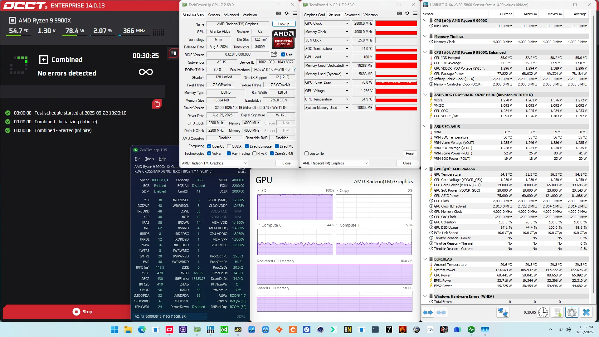
AMD Radeon Graphics (Granite Ridge): V/F Curve
Similar to other IP blocks and AMD graphics cards, the Radeon Graphics also have their own voltage-frequency curve.
At 2.2 GHz, we need about 1.045V. The lower voltage limit is 720 mV and the upper voltage limit is 1.25V. We hit this limit at about 2.5 GHz. Any frequency higher than 2.5 GHz is also restricted to the same 1.25V limit.
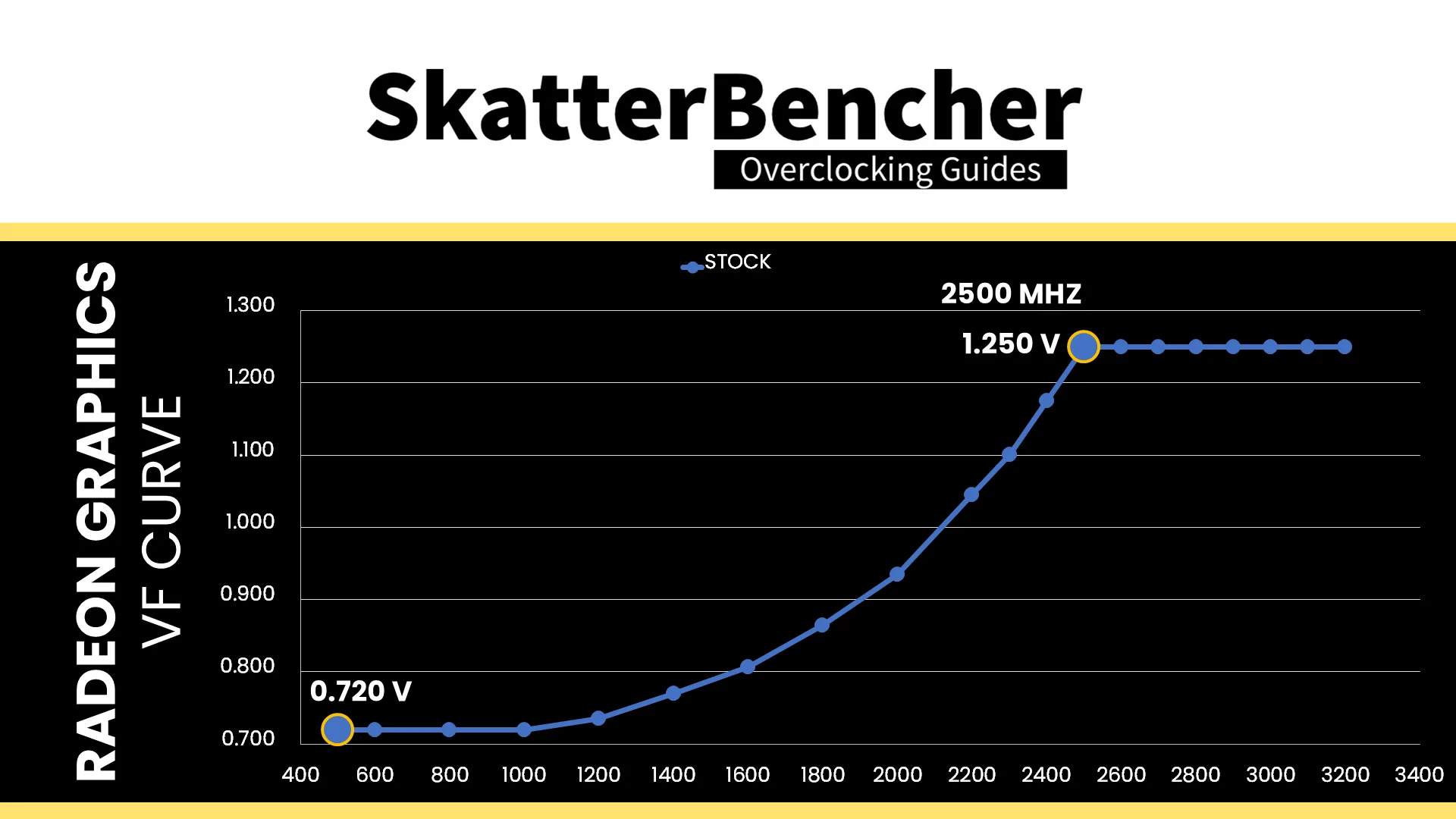
However, just like with AMD Ryzen CPUs, the voltage-frequency curve is really more of an abstraction than a set of programmed values. That’s because of AMD’s Adaptive Voltage Frequency Scaling technology.
Adaptive Voltage Frequency Scaling
Since 2015 and the Carrizo APU, AMD utilizes Adaptive Voltage Frequency Scaling, or AVFS. This technology relies on Critical Path Accumulators to estimate the maximum stable frequency of circuits inside your processor – whether a CPU or a GPU.
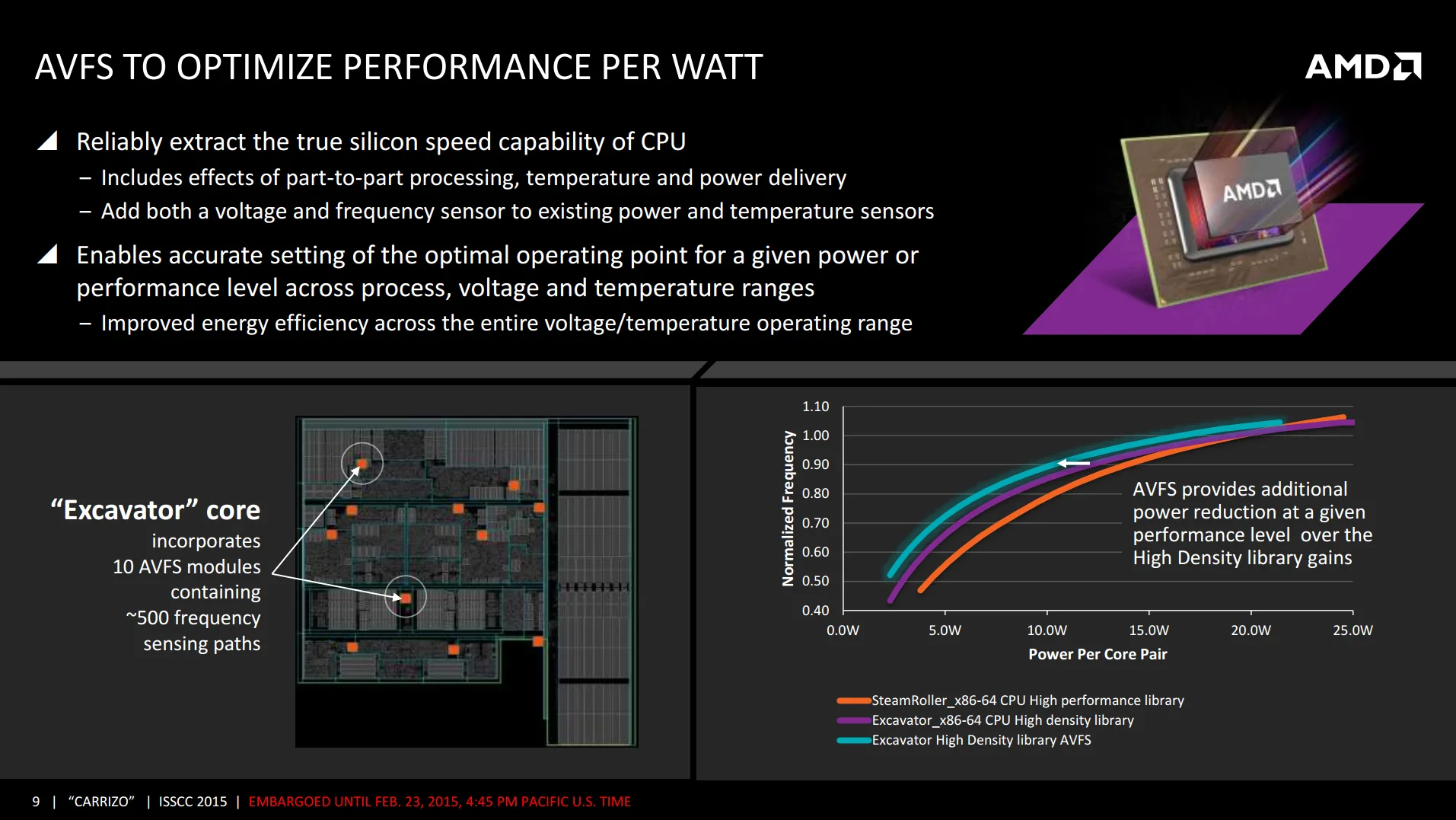
This is done by adding replica paths to the circuit that serve no purpose other than to assessing whether the circuit is stable. The AVFS technology then extracts a Gaussian distribution statistical model from the replicate paths and infers the stability of the “real” paths using sampling statistics. This statistical data is used by the SMU to create a Voltage-Frequency-Temperature (VFT) table.
The VFT table is a part-specific lookup table with information on the optimal voltage for any combination of frequency and voltage. The higher the frequency and temperature, the higher the required voltage to ensure stability.
Voltage Adaptive Operation
Despite advanced technologies like AVFS, AMD cannot predict what will happen in the real world. Sometimes, the voltage droop under transient conditions, going from idle to load or vice versa, is so significant that the system crashes.
Fortunately, AMD also has Voltage Adaptive Operation technology, commonly known as Clock Stretching. The technology consists of two circuits: one circuit serves as a configurable droop detector, and the second circuit functions as a configurable digital frequency synthesizer.
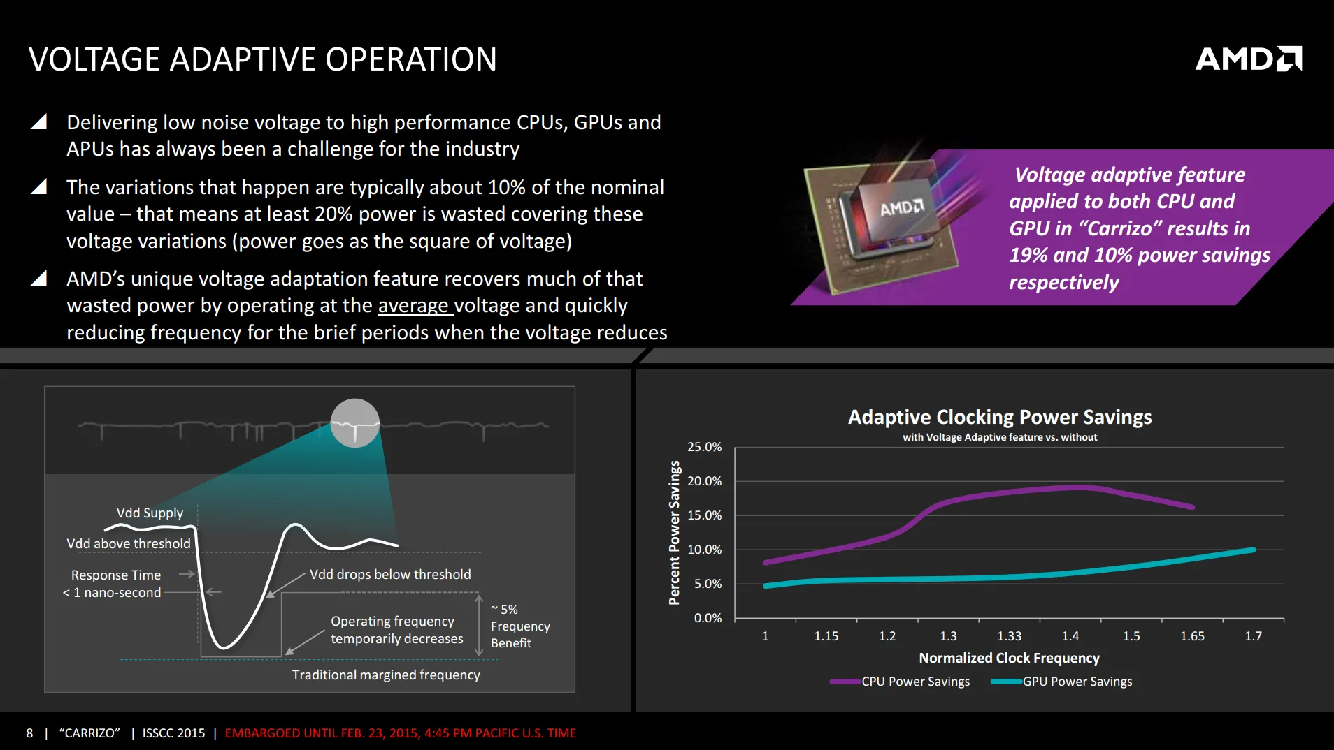
The idea is simple: since the operating frequency is tied directly to the voltage, if a voltage droop is detected, the effective clock frequency gets lowered to ensure continuous operation instead of a system crash. In the real world, this technology is incredibly relevant when overclocking because it may cause effective performance at a given frequency to be lower than expected.
The practical implication of voltage adaptive operation is that the effective clock frequency may differ from the configured clock frequency. How this works on AMD CPU and GPUs is slightly different, but it essentially boils down to this:
- The clock frequency is determined by the configured target frequency, which is often based on a reference clock and a multiplier. It’s usually the GPU frequency you’ll see in GPU-Z.
- The Effective Clock Frequency is the total clock cycles between two moments. This determines the actual performance as work gets done with each clock cycle. We can conveniently check the effective clock frequency with tools like HWiNFO.
For example, this screenshot shows that the set GPU clock is 2200 MHz, but the effective clock is 2223.4 MHz.
AMD GPUs heavily rely on the Voltage Adaptive Operation to continuously operate at the maximum possible frequency given a certain voltage level. You’ll find that in heavier workloads, which cause more Vdroop, the difference between the set target clock and the effective clock will be greater.
In some cases, we can take advantage of this technology. For example, with the Radeon RX 6500 XT, we overvolted the GPU, which caused the effective clock to be higher than the set target clock. We could reach a 3 GHz effective clock with a 2975 MHz set clock.
AMD Radeon Graphics (Granite Ridge): Tuning Process
If the theory feels a bit overwhelming, then I have good news. The practical side of overclocking the Radeon Graphics is much, much simpler. In fact, it’s really just a matter of increasing the GPU Clock Frequency until it’s unstable.
I found that the earliest sign of instability is getting artifacts on desktop. I got these around 2.9 GHz, so I settled for a GPU Clock Frequency of 2.8 GHz.
BIOS Settings & Benchmark Results
Upon entering the BIOS
- Go to the Extreme Tweaker menu
- Set Ai Overclock Tuner to EXPO I
- Enter the Precision Boost Overdrive submenu
- Set Precision Boost Overdrive to enabled
- Leave the Precision Boost Overdrive submenu
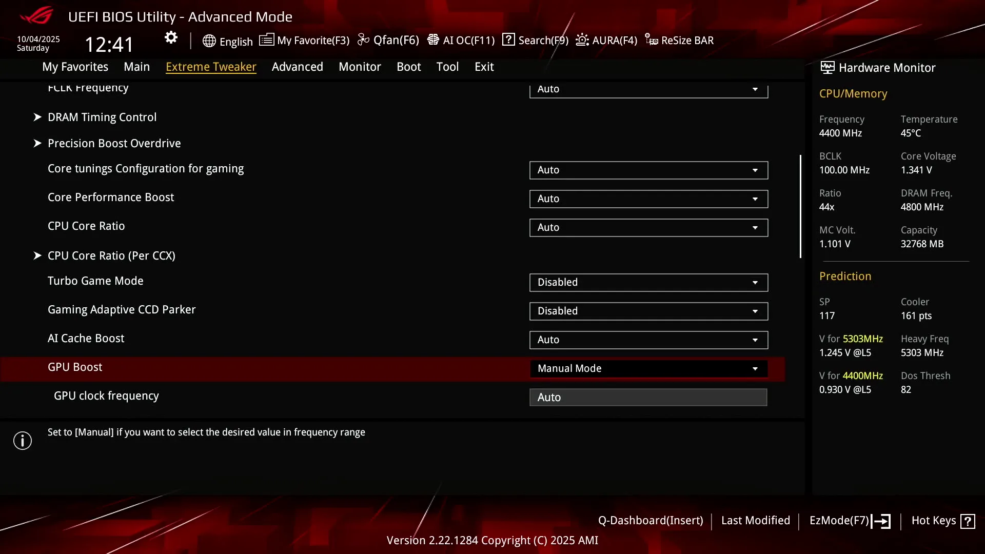
- Set GPU Boost to Manual mode
- Set GPU clock frequency to 2800
- Switch to the Advanced Menu
- Enter the NB Configuration submenu
- Set Primary Video Device to IGFX Video
- Set UMA Frame Buffer Size to 16G
Then save and exit the BIOS.
We re-ran the benchmarks and checked the performance increase compared to the default operation.
With a GPU frequency increase of about 27%, we’ll obviously get higher performance across our entire benchmark suite. It’s interesting to see the Memtest Vulkan Write and Checked bandwidth also scale significantly with increased GPU frequency. The Geomean performance speedup over stock is +35.21%, and we get a maximum benchmark speedup of +42.86% in Returnal.
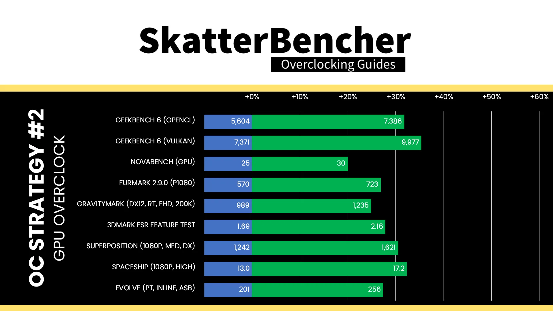
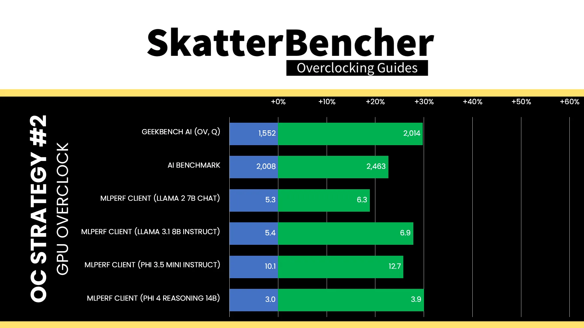
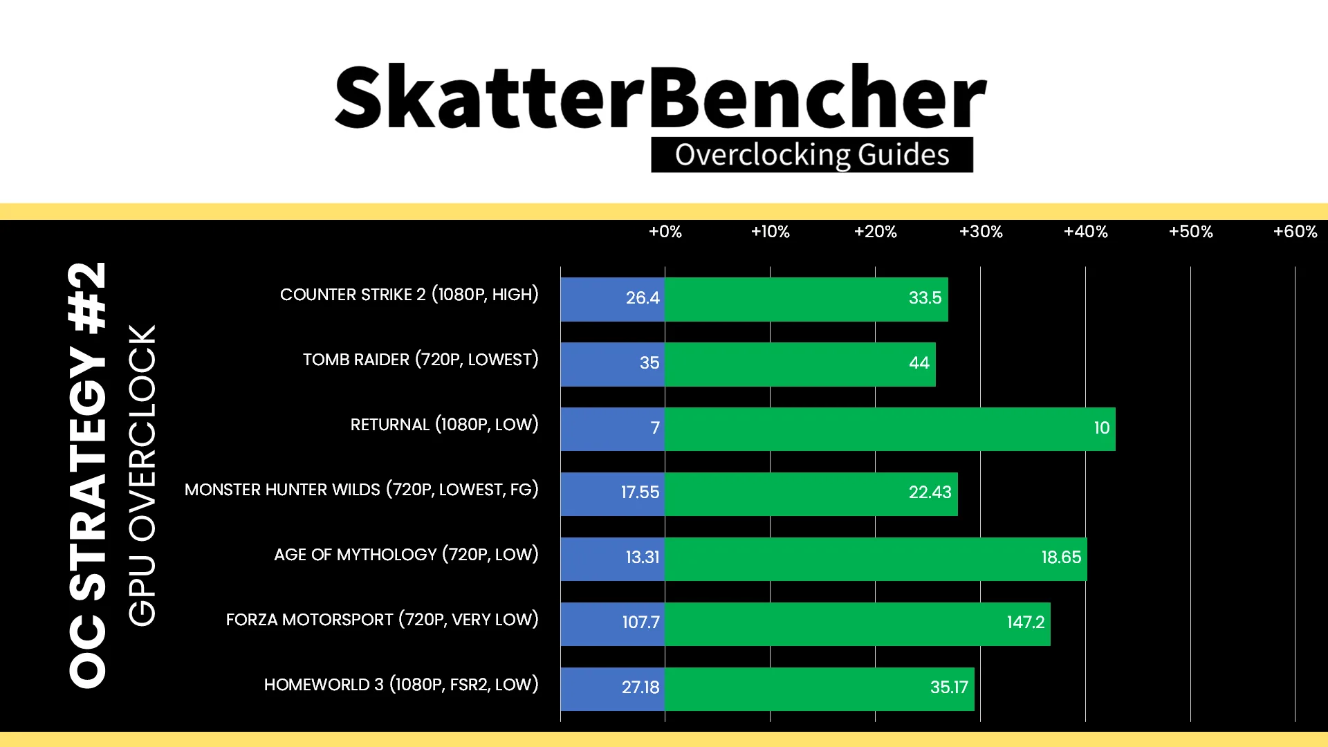
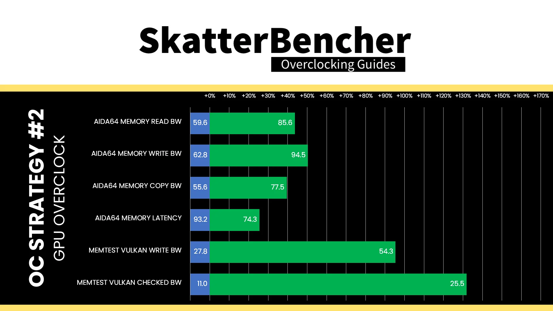
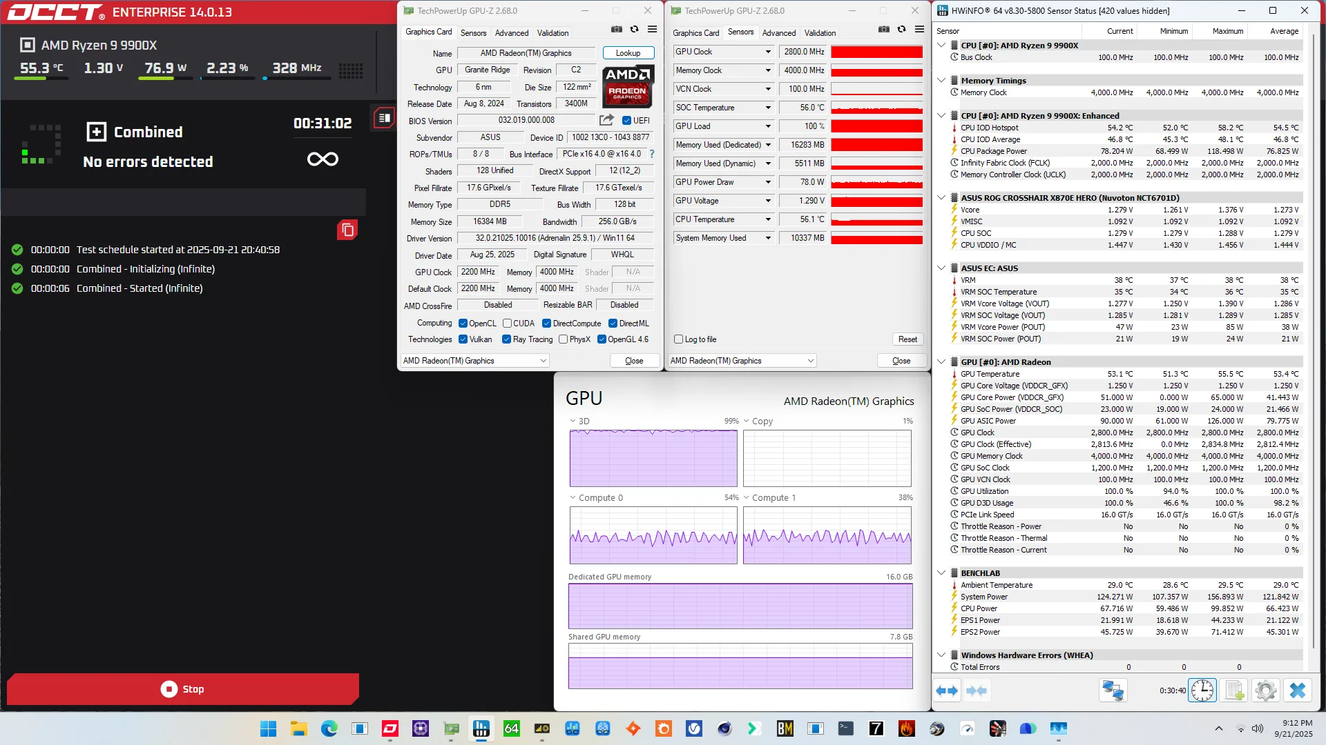
When running the OCCT 3D Adaptive and VRAM Combined Stress Test , the average GPU effective clock is 2812 MHz with 1.286 volts. The average GPU temperature is 53.4 degrees Celsius. The average GPU core power is 41.4 watts.
Higher Than Expected Voltage for CPU Cores?
I want to take a quick moment to highlight the impact of increasing the GPU frequency on the CPU core voltage. As we discussed already, the integrated graphics share the voltage rail with the CPU cores and all are in bypass mode. Therefore, when we increase the graphics frequency and its associated voltage, the CPU core voltage may also increase.
To illustrate this point, I ran the same configuration from SkatterBencher #92, OC Strategy #1, but with the integrated graphics enabled and running a light workload. This is the same system, same hardware.
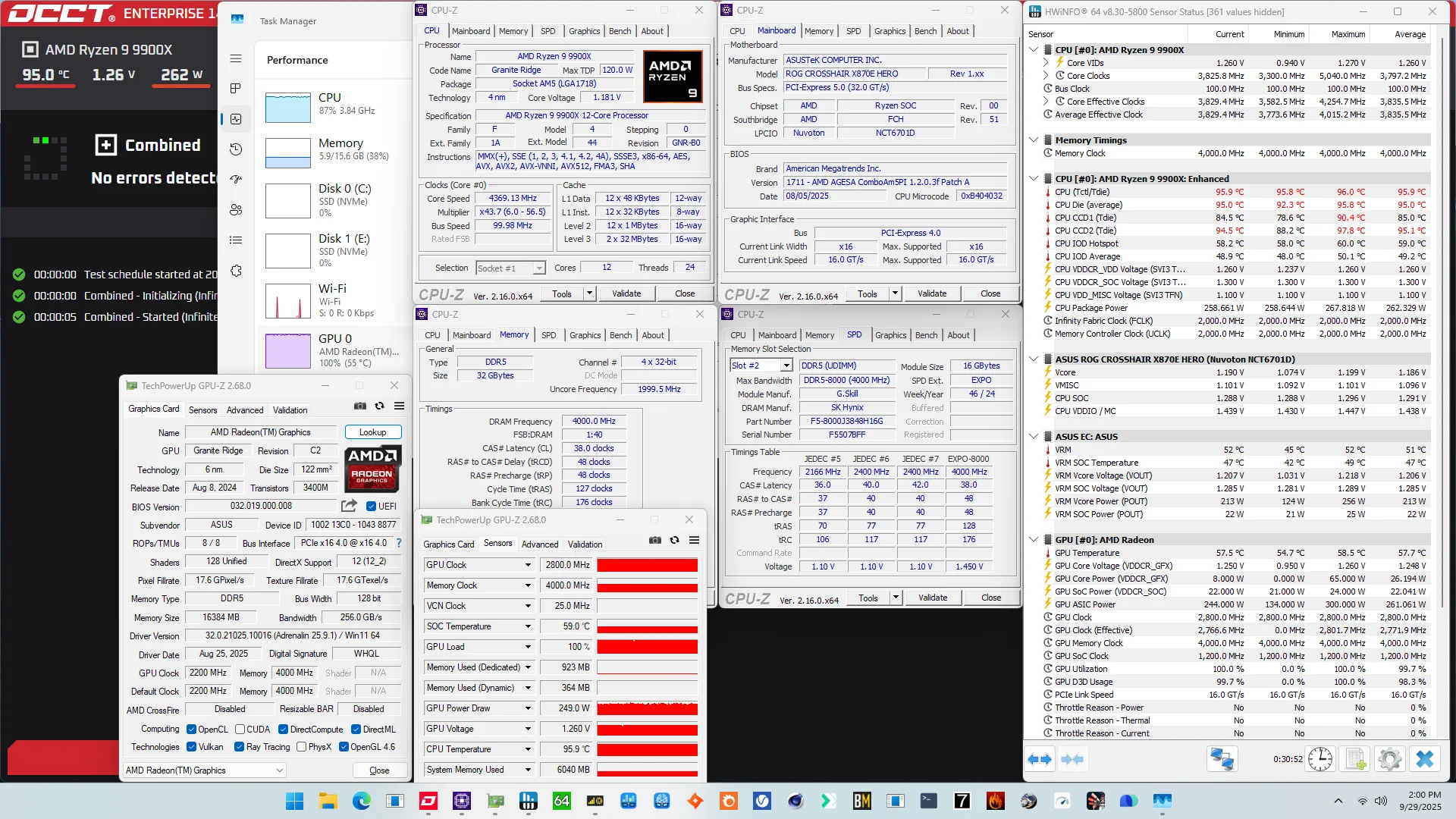
At first sight, nothing too spectacular: the package power increases 30W (262.2W vs 229.2W) and the temperature remains at 95°C. But the devil is in the details, because we can see the average VDDCR_VDD voltage is 100mV higher (1.26V vs 1.16V) due to the integrated graphics.
That increase in voltage triggers a number of Precision Boost performance limiters and we find the CPU cores running at almost 1.2 GHz lower frequency (3797 vs 4970 MHz)! So, be aware that running overclocked integrated graphics may significantly affect CPU performance in high load scenarios.
Sidenote: the main limiting factor of this test is the temperature limit. So, I might try liquid nitrogen to see how much we can push power consumption.
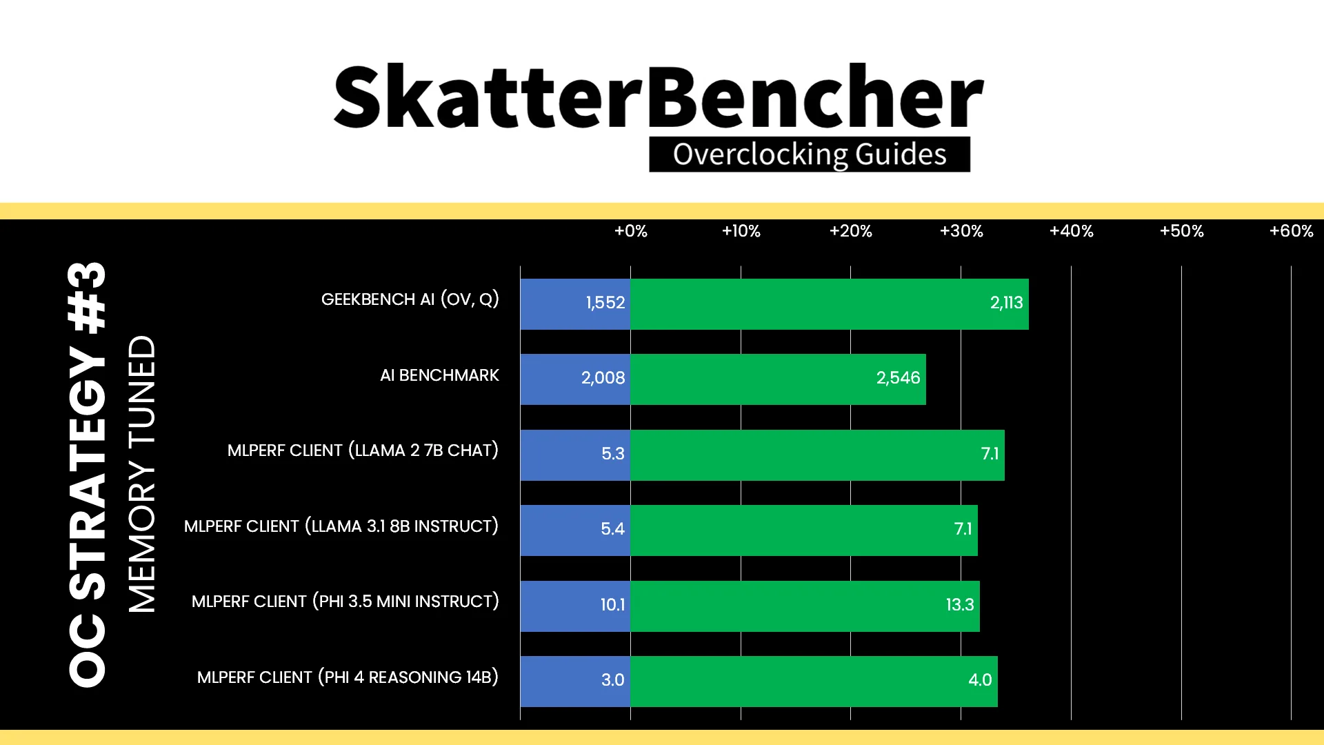
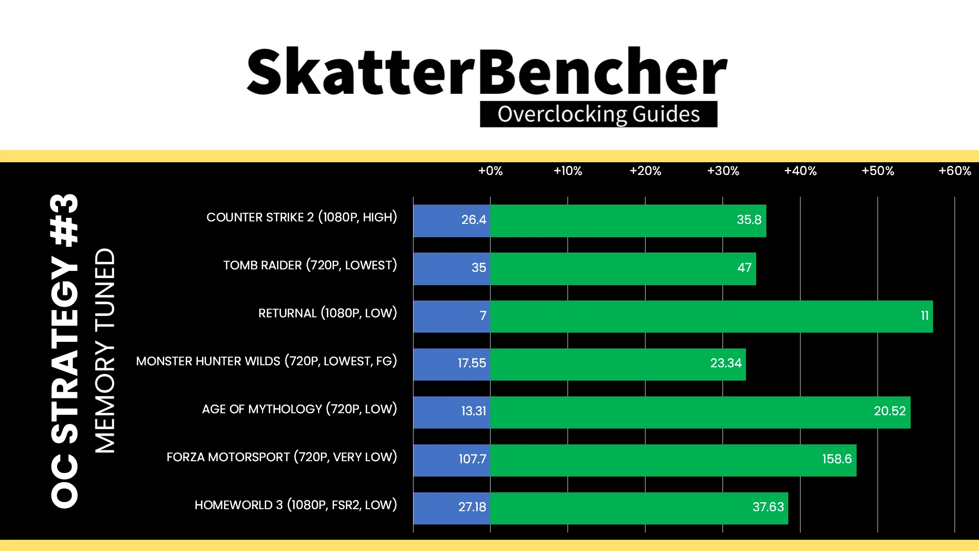
OC Strategy #3: Memory Tuned
In our third overclocking strategy, we delve into tuning the memory subsystem performance.
On AMD Granite Ridge processors, the memory subsystem consists of three major parts: the infinity fabric, the unified memory controller, and the system memory. They’re more commonly referred to as FCLK, UCLK, and MCLK. First-generation Ryzen overclockers know that these parts used to be tightly coupled together, but on modern Ryzen processors like the Ryzen 9 9900X, we can tune them independently.
Infinity Fabric Tuning
The Fabric frequency, or FCLK, is generated by the SOC PLL, derived from a 100 MHz reference clock input. The reference clock is multiplied by the FCLK ratio, which you can configure in the BIOS.
The standard operating frequency of the infinity fabric is 1800 MHz, but on many boards, you’ll find it runs at 2 GHz when Precision Boost Overdrive is enabled. Tuning the Infinity Fabric probably has a minimal impact on graphics performance because the graphics IP block is on the IO die, just like the memory controllers.
That said, it doesn’t seem there’s much overclocking headroom beyond 2 GHz. I managed to set 2200 MHz for this overclocking strategy, however anything higher couldn’t boot reliably. Not even with voltage adjustments.
Speaking of voltage: the infinity fabric voltage is provided by the VDDG voltage supply, derived via an integrated voltage regulator from the VDDCR_MISC voltage rail. There is a total of four VDDG voltage rails available for manual adjustment:
- CCD0-CCD VDDG: signals sent from CCD0 to IOD are sent at this voltage.
- CCD0-IOD VDDG: signals sent from IOD to CCD0 are sent at this voltage.
- CCD1-CCD VDDG: signals sent from CCD1 to IOD are sent at this voltage.
- CCD1-IOD VDDG: signals sent from IOD to CCD1 are sent at this voltage.
Note that the VDDG voltage does not adjust automatically with VDDCR_MISC. So, if you need to increase VDDG, for example, to support higher memory frequency, you need to change it manually.
Memory Controller Tuning
AMD Granite Ridge has two DDR5 Unified Memory Controllers, or UMC in short, and each provides two 32-bit memory channels. The memory controllers are located in the IO die and are identical to the memory controllers on Ryzen 7000 “Raphael” processors.
The Unified Memory Controller frequency, or UCLK, is derived from the UMCCLK, one of the SOC PLLs. The UMCCLK is driven by a 100 MHz reference clock derived from either an internal or external clock generator.
The memory controller frequency is tied directly to the system memory frequency. It can run either at the same or half its frequency. At default, the memory controller runs at the same frequency as the system memory at 2400 MHz. However, we find that when enabling EXPO, the motherboard auto-rules will drop the memory controller frequency to half the memory frequency.
We could easily force the memory controller to run at the same frequency as the system memory by setting UCLK DIV1 Mode to UCLK=MEMCLK. However, that’s only possible if we run the memory at around DDR5-6000. Since our memory is running at DDR5-8000, we’re forced to maintain a UCLK frequency that’s half that of the memory frequency.
The VDDCR_SOC voltage rail provides the external power for multiple internal voltage regulators on SOC for the various IP blocks, including the memory controller. The VDDIO_MEM voltage rail is related as it provides the external power for the VDDP DDR5 bus signaling.
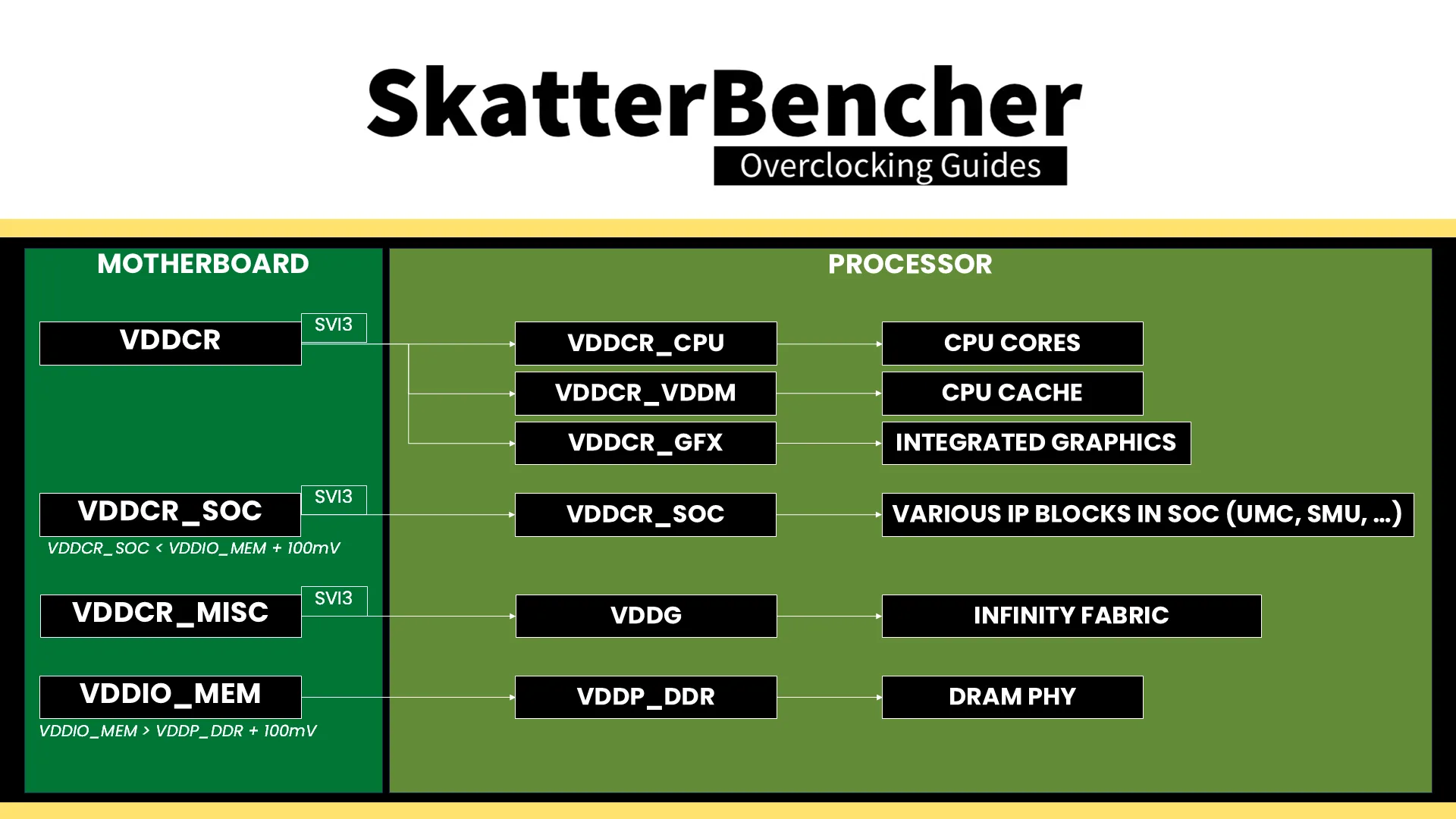
It is essential to know that the VDDCR_SOC voltage must always be lower than VDDIO_MEM_S3 + 100mV. The default VDDCR_SOC voltage is 1.05V and can be set to 1.30V under ambient conditions. That’s typically required for running the memory controller in sync with the memory at DDR5-6400. However, we need LN2 mode enabled for higher voltages.
System Memory Timings Tuning
The last piece of the memory subsystem performance tuning is tuning the memory timings. For this part, I rely in part on ASUS’ Memory Presets technology.
ASUS Memory Presets
ASUS Memory Presets is an ASUS overclocking technology that provides a selection of memory-tuning presets for specific memory ICs. The presets will adjust the memory timings and voltages.
The ROG Crosshair X870E Hero motherboard sports fourteen memory profiles for a variety of memory ICs and configurations. Since we’re interested in simply adjusting the memory timings, we can try the Hynix 7600MHz 1.45V 2x16GB SR preset.
Memory Timings Tuning
The Hynix 7600 memory preset turned out not to be stable as it would throw errors in the OCCT Memory Stress test almost instantly. But no cause for alarm because we’ve seen this in previous overclocking guides as well.
To fine-tune the timings, I try setting certain timings back to its EXPO value until I find the timings that caused the errors. To speed up the process, I group together the following timings:
- Group 1: primary timings plus tRC
- Group 2: all refresh-related timings
- Group 3: tWR, tFaw, twrrd, and trdwr
- Group 4: all -Scl, -Sc, -Sd, and -dd secondary timings
- Group 5: TrrdL, TrrdS, TwrtL, TwtrS
Unfortunately, unlike with previous overclocking guides, I had to adjust quite a lot more timings to make the memory pass our target of 1 hour of OCCT stress testing. Here are the final optimized memory timings for this memory kit.
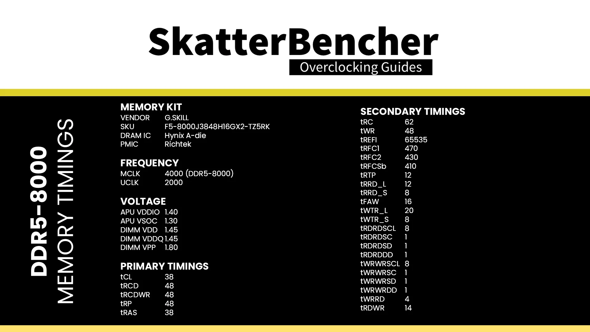
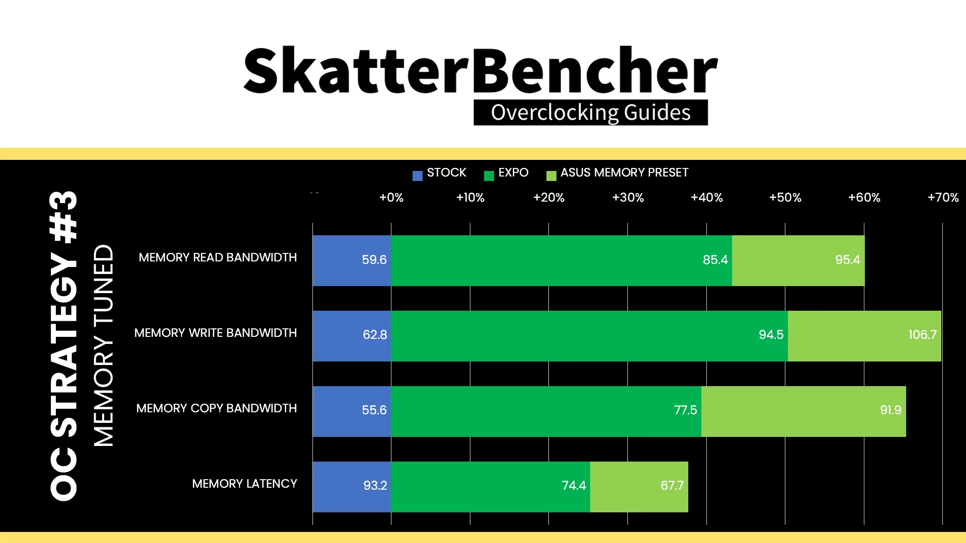
After the memory subsystem tuning, our AIDA64 performance improved quite significantly. We got about +40% extra bandwidth and 20% lower latency by enabling EXPO. The memory tuning then added another 20% improvement on top of that.
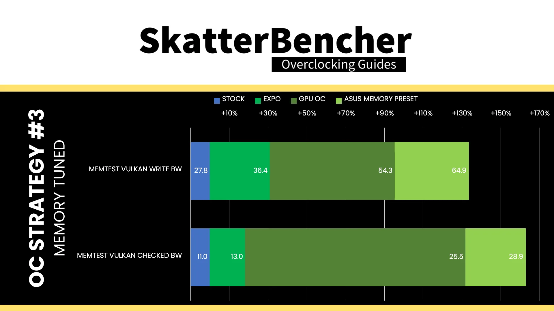
The Memtest Vulkan performance also improves another 30-40% though the biggest gains come from overclocking the GPU.
BIOS Settings & Benchmark Results
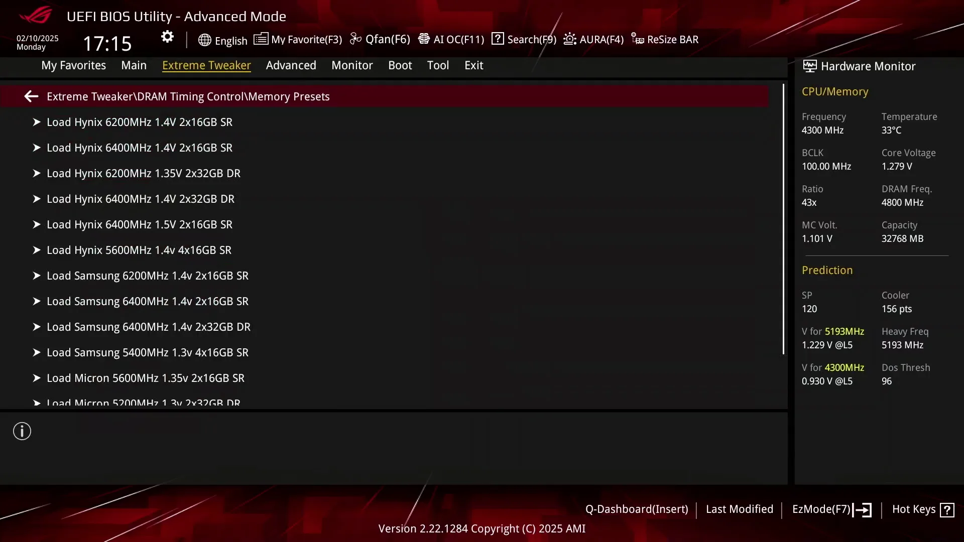
Upon entering the BIOS
- Go to the Extreme Tweaker menu
- Set Ai Overclock Tuner to EXPO I
- Set FCLK Frequency to 2200 MHz
- Enter the DRAM Timing Control submenu
- Enter the Memory Presets submenu
- Select Load Hynix 7600MHz 1.45V 2x16GB SR and click OK
- Leave the Memory Presets submenu
- Set tCL to 38
- Set tRCD WR to 48
- Set tRCD RD to 48
- Set tRP to 48
- Set tRRDL to 12
- Set tRDDS to 8
- Set tWRTL to 20
- Set tWRTS to 8
- Enter the Memory Presets submenu
- Leave the DRAM Timing Control submenu
- Enter the Precision Boost Overdrive submenu
- Set Precision Boost Overdrive to enabled
- Leave the Precision Boost Overdrive submenu
- Set GPU Boost to Manual mode
- Set GPU clock frequency to 2800
- Switch to the Advanced Menu
- Enter the NB Configuration submenu
- Set Primary Video Device to IGFX Video
- Set UMA Frame Buffer Size to 16G
Then save and exit the BIOS.
We re-ran the benchmarks and checked the performance increase compared to the default operation.
As we’ve seen with other integrated graphics, tuning the memory timings can have significant impact on performance, especially in workloads which are memory dependent like games and AI workloads. The Geomean performance speedup is +46.01%, and we get a maximum benchmark speedup of +57.14% in Returnal.
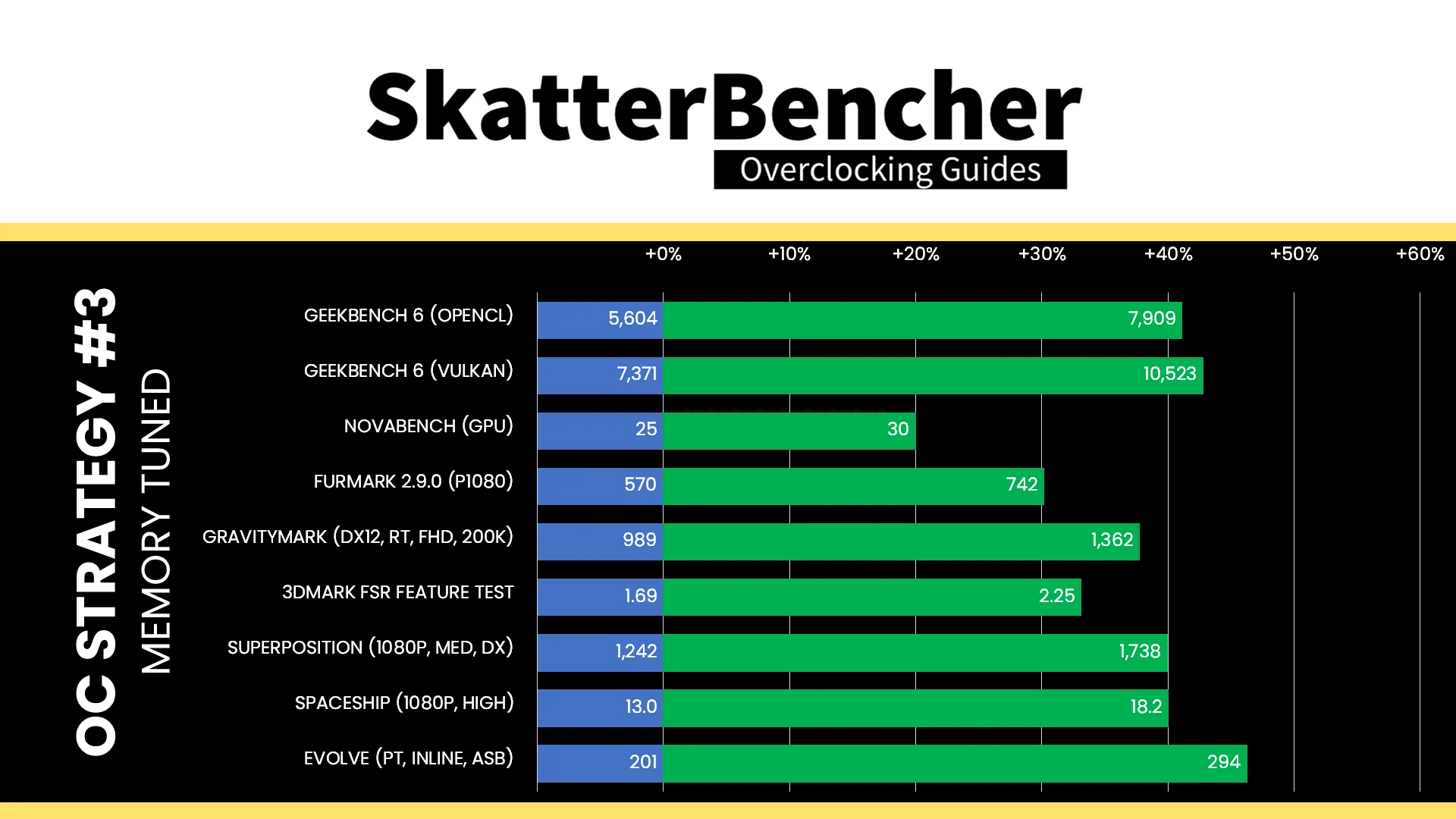

When running the OCCT 3D Adaptive and VRAM Combined Stress Test , the average GPU effective clock is 2814 MHz with 1.285 volts. The average GPU temperature is 54.1 degrees Celsius. The average GPU core power is 43.6 watts.
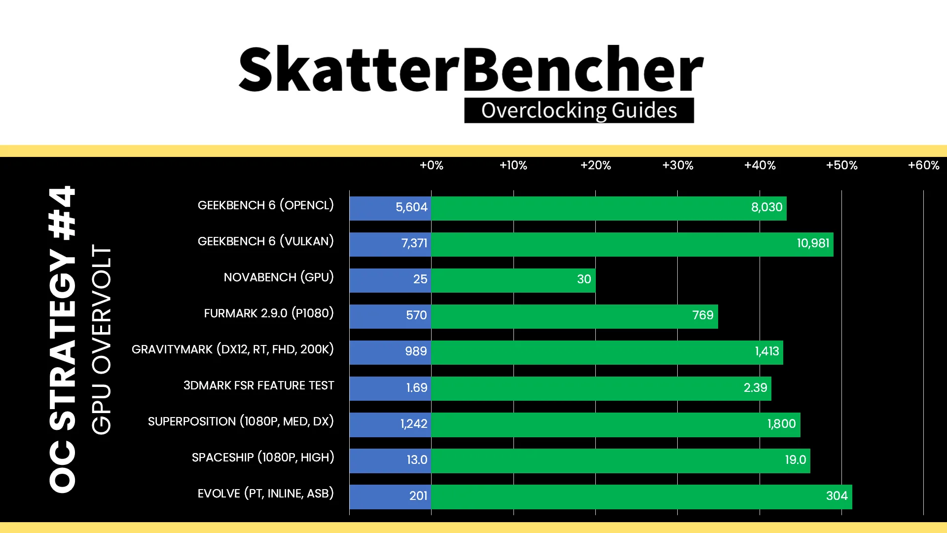
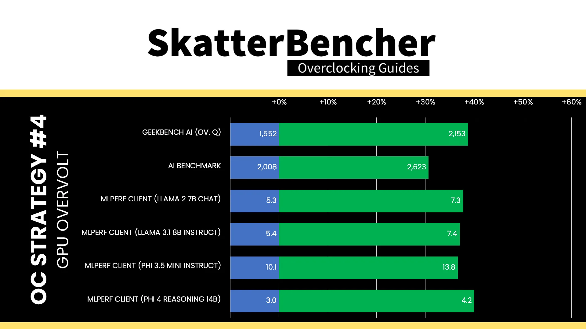
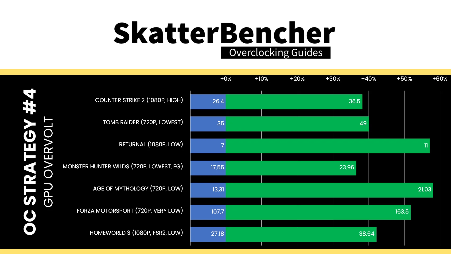
OC Strategy #4: GFX Curve Optimizer
In our final overclocking strategy, we do everything we can to squeeze more frequency out of the GPU including overvolting using Curve Optimizer.
PBO 2: GFX Curve Optimizer
Curve Optimizer is one of the most important overclocking tools of the Precision Boost Overdrive 2 toolkit. It is most commonly known for its CPU core undervolting capabilities, but on AMD Ryzen 9000 CPUs it’s also available for the Radeon Graphics.
To explain how it works, let’s start with the basics: the voltage-frequency curve.
Here’s the default voltage-frequency curve of the Radeon Graphics. We can immediately make a simple and redundant observation: the higher the frequency, the higher the voltage. For example: for 2 GHz we only need 0.935V, but for 2.5 GHz we need 1.25V.
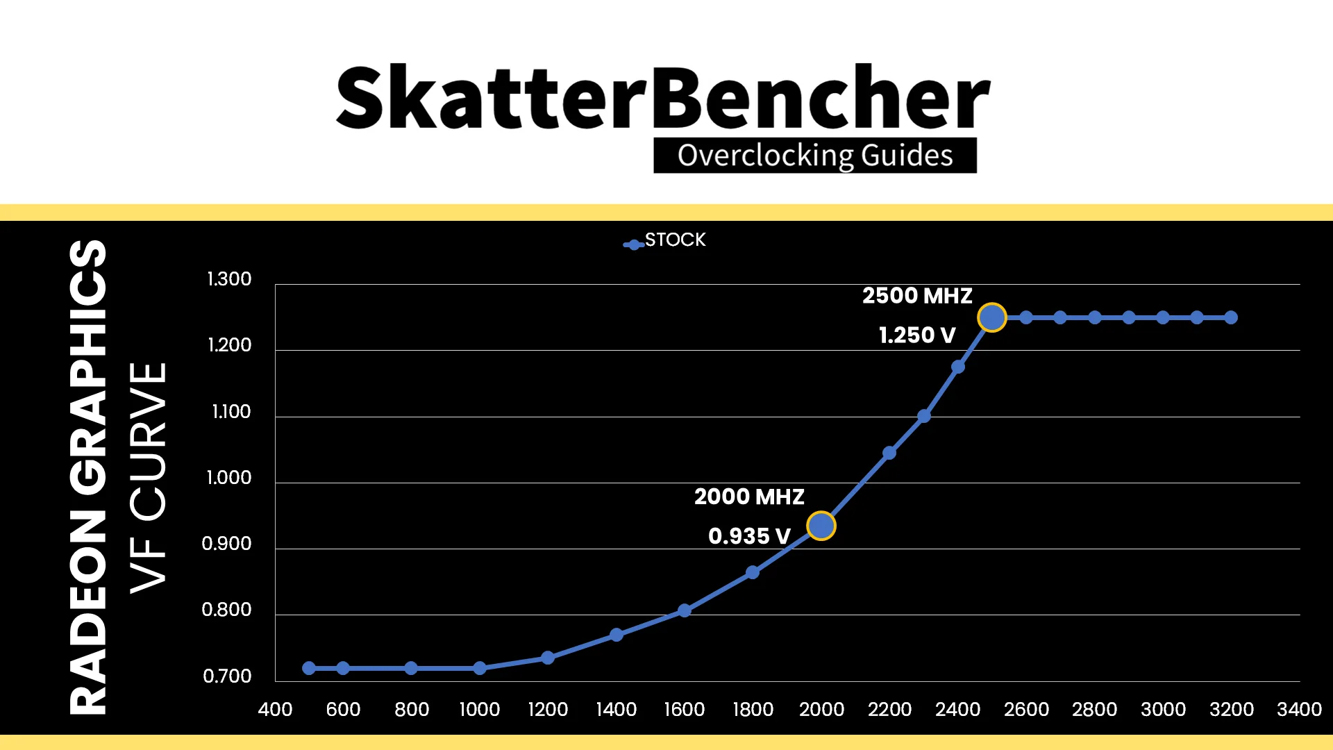
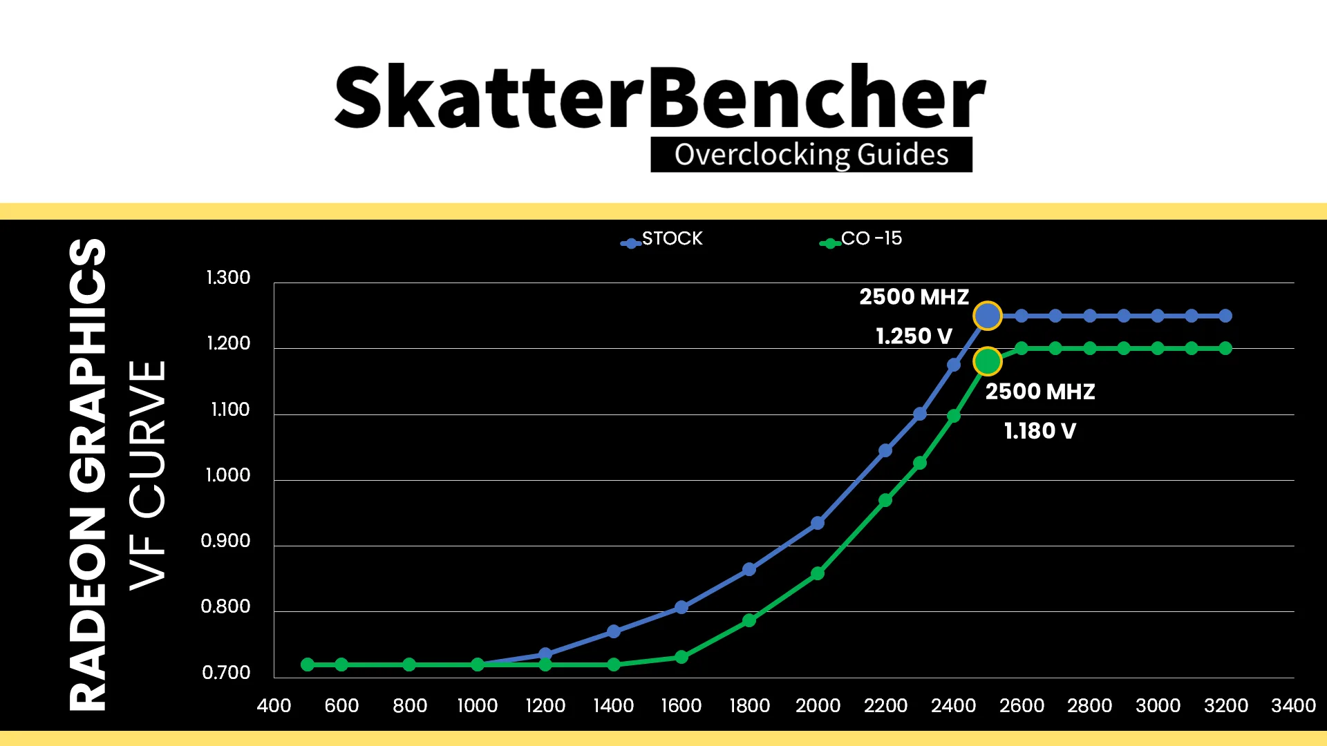
If we set a negative Curve Optimizer, we can shift the entire voltage-frequency curve along the voltage axis. And, suddenly, we need less voltage for every operating frequency. For example, at default, for 2.5 GHz we needed 1.25V but with a -15 Curve Optimizer we only need 1.18V! Similarly, a positive Curve Optimizer will make us use more voltage for every operating frequency.
We can use this tool to try to stabilize higher frequencies at 1.25V. In my case, I set the GPU frequency to 3 GHz and a +20-curve optimizer. That yields an effective clock frequency of over 2.9 GHz in our OCCT stress test.
OC Mode & Manual Voltage
Some might be thinking: why not manually set the VDDCR_VDD voltage? That’s a solid idea because it would give us direct control over the graphics voltage. Unfortunately, it turns out that increasing the operating voltage doesn’t seem to increase stability above 3 GHz. In fact, we run into the same desktop artifacts as we do with dynamic voltage.
I assume that means we’re hitting the frequency limit at ambient temperature. Maybe I’ll have a look at what we can do with liquid nitrogen in the near future.
BIOS Settings & Benchmark Results
Upon entering the BIOS
- Go to the Extreme Tweaker menu
- Set Ai Overclock Tuner to EXPO I
- Enter the DRAM Timing Control submenu
- Enter the Memory Presets submenu
- Select Load Hynix 7600MHz 1.45V 2x16GB SR and click OK
- Leave the Memory Presets submenu
- Set tCL to 38
- Set tRCD WR to 48
- Set tRCD RD to 48
- Set tRP to 48
- Set tRRDL to 12
- Set tRDDS to 8
- Set tWRTL to 20
- Set tWRTS to 8
- Enter the Memory Presets submenu
- Leave the DRAM Timing Control submenu
- Set GPU Boost to Manual mode
- Set GPU clock frequency to 3000
- Switch to the Advanced Menu
- Enter the NB Configuration submenu
- Set Primary Video Device to IGFX Video
- Set UMA Frame Buffer Size to 16G
- Leave the NB Configuration submenu
- Enter the AMD Overclocking submenu and click accept
- Enter the DDR and Infinity Fabric Frequency/Timings submenu
- Enter the Infinity Fabric Frequency and Dividers submenu
- Set Infinity Fabric Frequency and Dividers to 2200 MHz
- Leave the Infinity Fabric Frequency and Dividers submenu
- Enter the Infinity Fabric Frequency and Dividers submenu
- Leave the DDR and Infinity Fabric Frequency/Timings submenu
- Enter the Precision Boost Overdrive submenu
- Set Precision Boost Overdrive to Advanced
- Set PBO Limits to Motherboard
- Enter the GFX Curve Optimizer submenu
- Set GFX Curve Optimizer to GFX Curve Optimizer
- Set GFX Curve Optimizer Sign to Positive
- Set GFX Curve Optimizer Magnitude to 20
- Set GFX Curve Optimizer to GFX Curve Optimizer
- Enter the DDR and Infinity Fabric Frequency/Timings submenu
Then save and exit the BIOS.
We re-ran the benchmarks and checked the performance increase compared to the default operation.
By marginally increasing the effective clock frequency, we get a minor bump in performance in most of our benchmark workloads and games. The Geomean performance speedup over stock is +49.85%, and we get a maximum benchmark speedup of +58.08% in Age of Mythology.

When running the OCCT 3D Adaptive and VRAM Combined Stress Test , the average GPU effective clock is 2915 MHz with 1.269 volts. The average GPU temperature is 53.8 degrees Celsius. The average GPU core power is 37.9 watts.

AMD Radeon Graphics (Granite Ridge): Conclusion
Alright, let’s wrap this up.
Overclocking the Radeon Graphics integrated in the Ryzen 9000 CPUs is a bit of an academic exercise. Yes, it’s possible. Yes, there’s quite a bit of headroom. And, yes, there’s an impressive performance bump. But double of almost nothing is still almost nothing.
However, it was interesting to see how overclocking the integrated graphics can affect CPU core performance due to the shared VDDCR voltage rail. In a worst case, heavy load scenario, overclocking the GPU by 300 MHz can reduce the CPU frequency by more than 1 GHz. That’s not a common scenario, but still. Perhaps it’s time to consider giving even the tiny integrated graphics its own voltage rail. And maybe also upgrade to RDNA 4 while we’re at it.
Anyway, that’s it for this guide. Let me know in the comments if you want me to try overclocking the integrated graphics with liquid nitrogen!
I want to thank my Patreon supporters and YouTube members for supporting my work. If you have any questions or comments, please drop them in the comment section below.
See you next time!
PieterIsSoCool
thanks for the clarification! i did observe a case of my 7000-series igpu seemingly reaching higher reported gfx voltage than vsoc by a considerable margin, which was a bit puzzling. though in most cases it does seem to stay under vsoc.
PieterIsSoCool
did the gfx voltage topology change from 7000 to 9000, or was your earlier topology interpretation incorrect?
Pieter
I think my previous interpretation was incorrect