Alder Lake Overclocking: What’s New

Alder Lake is finally here and just like with every new generation, a new CPU means new overclocking features.
Intel Alder Lake is the 12th generation of Intel Core processors built on the Intel 7 process technology. It’s Intel’s first high-performance hybrid architecture for mainstream desktops. Very much unlike previous launches, Intel’s pushing out the enthusiast K CPUs and Z motherboards a couple of months before the mainstream parts.
In this article, we’ll dig into everything new about overclocking Alder Lake. We’ll dig into the following topics:
- The Alder Lake architecture and highlight the things that are important for performance enthusiasts and overclockers
- Alder Lake processor and ring overclocking, including the P-cores and the E-cores
- Integrated graphics overclocking
- DDR4 and DDR5 memory overclocking
- Other small topics about overclocking
- ASUS ROG Maximus Z690 Extreme overclocking tools
- Lastly, let’s talk about some overclocking expectations for both ambient and extreme
Alright, we have lots to cover so let’s get straight to it.
Intel Alder Lake Architecture
Intel Alder Lake is the 12th generation Intel Core processor which features an all-new core design with performance hybrid architecture and Intel Thread Director. It’s built on the Intel 7 process technology formerly known as 10nm Enhanced SuperFin (ESF). It’s a scalable SoC architecture which means Alder Lake will cover all client segments from 9W for ultra-thin notebooks to 125W for gaming and workstation desktops.
Well … 125W+.

Alder Lake also comes with some of the most advanced memory and I/O including DDR5, PCIe Gen 5, Thunderbolt 4, and Wi-Fi 6E.
When it comes to the K-SKU desktop CPUs, the most important novelty is the introduction of the hybrid design with performance-cores, or P-cores, and efficient-cores, or E-cores.
The Performance-cores are based on the Golden Cove architecture which succeeds Tiger Lake’s Willow Cove on mobile and Rocket Lake’s backported 14nm version called Cypress Cove. The Golden Cove core is the same that’s supposed to end up in the next-generation Xeon processors codenamed Sapphire Rapids.
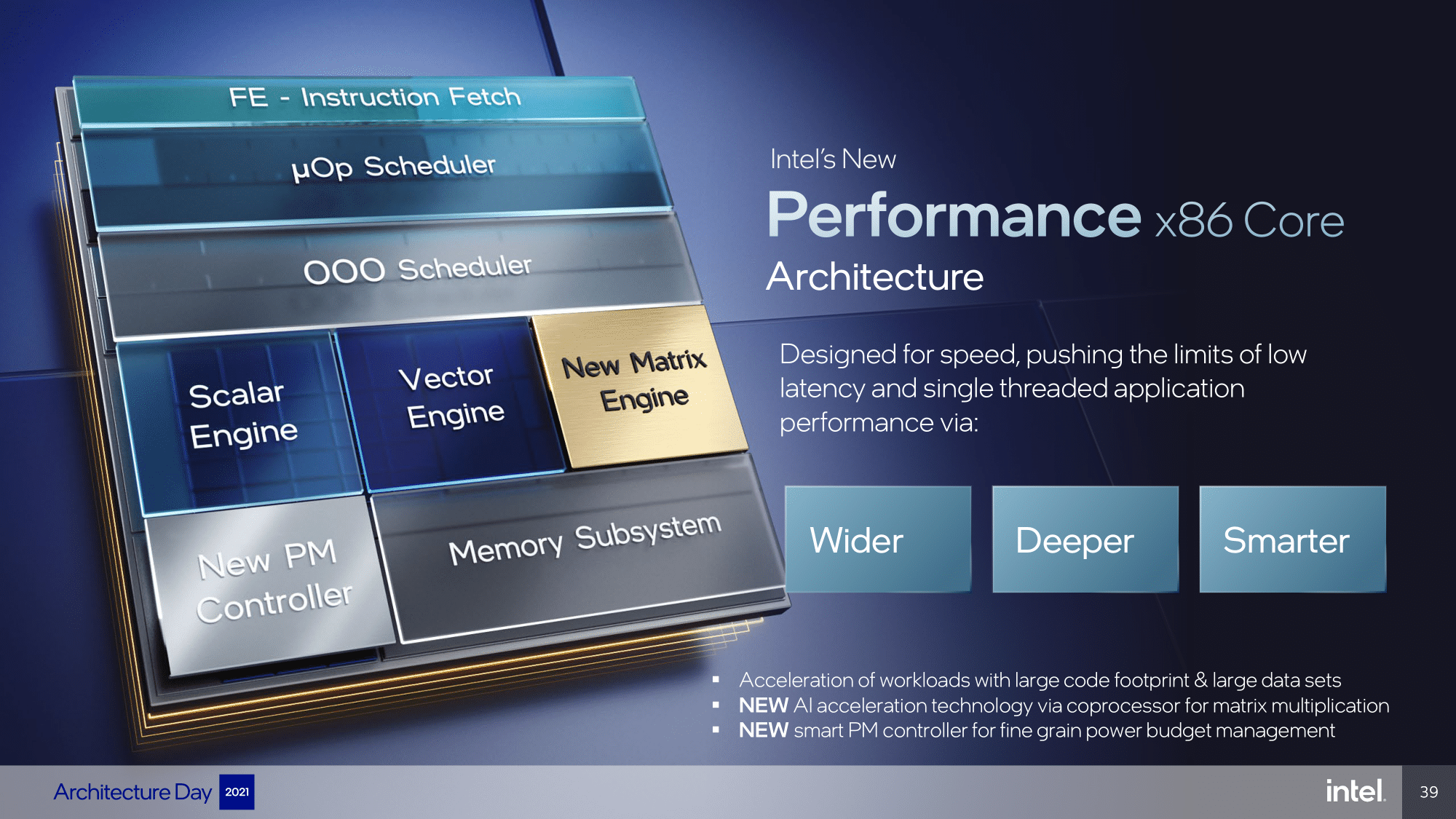
Intel shared a lot of information on Golden Cove during the Intel Architecture Day 2021 event. The main takeaway is that Golden Cove is a major update to the core microarchitecture and offers up to a 19% IPC increase over Cypress Cove. Then, it also has a bunch of additional improvements for AI and deep learning workloads.
The Efficient-cores are based on the Gracemont microarchitecture which succeeds Jasper Lake’s Tremont on low-power devices. The Efficient-cores are optimized for power and density efficient throughput as opposed to the Performance-cores which are optimized for maximum performance.

From an enthusiast’s perspective, there isn’t much exciting about the Efficient-cores other than they enable higher multi-threaded performance. Intel claims the Efficient-cores provide over 40% more performance at 40% lower power than Skylake in single-threaded applications and over 80% more performance at 80% lower power in multi-threaded applications. If you want to know more about this, I’m sure there are plenty of media out there that did the testing.
One interesting insight from the Intel Architecture day is that the 4MB L2 cache is shared among four E-cores. This will come back later when we talk about overclocking the CPU cores.

Note that Alder Lake does not officially support AVX-512. Although it had been mentioned in certain documentation that the P-cores are AVX-512 capable, it looks like the functionality has been disabled. Well, let’s talk about it later.
And that’s about it. To summarize, for overclockers and enthusiasts the most exciting things are:
- New process technology for desktop CPUs (not counting the Tiger Lake and 11900KB)
- New Golden Cove P-cores
- New Gracemont E-cores
- New DDR5 technology
Intel Alder Lake K-SKU Processors
The overclockable K-SKU processors again come in three flavors: Core i9, Core i7, and Core i5. Each of the three flavors has a -K a -KF variant. The only difference between the two variants is that the -KF comes without integrated graphics.
The Core i9-12900K processor has 8 P-cores and 8 E-cores with a total of 24 threads. The base frequency is 3.2 GHz for the P-cores and 2.4 GHz for the E-cores. The maximum single-core boost frequency is 5.1 GHz for the P-cores and 3.9 GHz for the E-cores. The favored P-cores can boost 100 MHz higher to 5.2 GHz. The processor base power is 125W and the maximum turbo power is 241W.
The Core i7-12700K processor has 8 P-cores and 4 E-cores with a total of 20 threads. The base frequency is 3.6 GHz for the P-cores and 2.7 GHz for the E-cores. The maximum single-core boost frequency is 4.9 GHz for the P-cores and 3.8 GHz for the E-cores. The favored P-cores can boost 100 MHz higher to 5.0 GHz. The processor base power is 125W and the maximum turbo power is 190W.
The Core i5-12600K processor has 6 P-cores and 4 E-cores with a total of 16 threads. The base frequency is 3.7 GHz for the P-cores and 2.8 GHz for the E-cores. The maximum single-core boost frequency is 4.9 GHz for the P-cores and 3.6 GHz for the E-cores. There are no favored cores on the 12600K as it does not support Turbo Boost Max 3.0. The processor base power is 125W and the maximum turbo power is 150W.
The integrated graphics included in the Alder Lake desktop CPUs is the Intel UHD Graphics 770. The architecture is identical to Rocket Lake though there are a couple of minor feature upgrades. The desktop CPU integrated graphics has up to 32 execution units. The base clock frequency is 300 MHz and the turbo boost frequency is 1550MHz.

Intel only allows for the Intel Xe graphics branding to be used for integrated graphics which have over 80 execution units and have dual-channel memory. As the desktop CPUs only have 32 EUs, the integrated graphics are not Xe graphics but keep the UHD Graphics branding.
Alder Lake fits the LGA1700 socket and will work on 600 series and possibly future 700 series motherboards. The LGA1700 socket should also be compatible with Alder Lake’s successor Raptor Lake which is rumored to arrive in the 2nd half of next year. Though while motherboards should offer an upgrade path, it may be useful to pair the next-gen CPU with a next-gen motherboard.

Alder Lake Overclocking: Clocking & Voltage Topology
Before we get to the overclocking, let’s first have a look at the Alder Lake Topology for both the clocking and voltage.
Intel Alder Lake Clocking
The clocking of Alder Lake is more similar to Tiger Lake than it is to Rocket Lake as it inherits the CPU internal clock generator from Tiger Lake. The standard Alder Lake platform has a 38.4MHz crystal as a reference clock to the PCH. The PCH will then generate 3 clocks:
- 38.4 MHz reference clock for the CPU internal clock generator
- 100MHz PCIBCLK for PCIe, DMI, and I/O
- 24MHz frequency for TSC, display, and SVID controller
The CPU internal clock generator then generates the 100MHz base clock frequency used for all the parts inside the CPU. This is different from Rocket Lake where the PCH PLL would generate the 100MHz base clock frequency with no interference from the CPU.
The main reason for including the internal clock generator would be to provide a cost-saving opportunity for low-cost systems or platforms.
However, just like Rocket Lake, on high-end desktop motherboards, you’ll still find an external clock generator feeding the 100MHz BCLK frequency to the CPU.
There doesn’t seem to be any obvious difference between using the internal or external clock generator, though motherboard vendors will argue the external clock generator will offer greater granularity and/or range.
Whichever way you get the 100 MHz BCLK, this clock is multiplied with specific ratios for each of the different parts in the CPU.


Each P-core has its own PLL and can run at its independent frequency. This is pretty much identical to Rocket Lake. However, things are a bit different for the E-cores as they are grouped in clusters of 4. The maximum supported ratio is up to 120X though I doubt anyone will ever get there.
While the technical documentation references a separate ratio for the E-cores L2 cache, it appears that the Atom L2 cache frequency is linked to the Atom cluster.
The Ring frequency ties together the Ring, last-level cache (L3), and CBo or Cache box. The Ring ratio can go up to 85X, but again I don’t think anyone will need ratios that high.
The GT frequency or graphics frequency is based on the same 100MHz BCLK but first divides it by 2 and then multiplies it with the GT ratio. Similar to Rocket Lake it appears that Slice and Unslice frequency are synced, but we’ll get back to that later in this video.
The GT ratio can go up to 42X and while on Rocket Lake this was more than sufficient to achieve the highest OC frequency, on Alder Lake that’s not quite the case.
The System Agent ratio is either 16X or 32X.
Finally, the two memory controllers and system memory are driven by the same 100 MHz BCLK, however, also support 133 MHz as base frequency. The 133 MHz is derived from the 100MHz BCLK which is first multiplied by 4 then divided by 3, and the memory controller drives the clock frequency for the system memory.
The Alder Lake memory controller supports gear down mode which effectively halves the memory throughput. In gear-down mode, the memory controller frequency is also halved and thus runs at half the frequency of the system memory. On Alder Lake, there’s now an additional gear down – Gear 4 – which makes the memory controller frequency run at a quarter of the memory speed. This can be useful for DDR5 overclocking.
The memory ratio goes up to 63X and combined with the 133 MHz frequency thus results in up to DDR4-8400 or DDR5-16800.


Intel Alder Lake Voltage
While Alder Lake clocking resembles Tiger Lake more than Rocket Lake, in the voltage department things are not quite that similar.
Compared to Tiger Lake, Alder Lake transitions away from using FIVR for the Cores, Ring, and integrated graphics. Instead, power gates are used. However, unlike Rocket Lake some parts of the Alder Lake CPU are powered using a FIVR.

Another major change is that, on DDR5 motherboards, the voltage for the memory ICs is now provided by the PMIC on the memory sticks. Previously, there would be a dedicated voltage regulator on the motherboard. The PMIC provides the VDD, VDDQ, and VPP voltage to the memory ICs.

If we only consider the Alder Lake CPU and disregard the chipset, there are a total of 7 different voltage inputs.
Let’s go over them one by one.
- VccGT: this voltage powers the GT or integrated graphics including the Slice, Unslice, and Display block. It supports both override and adaptive voltage mode
- VccIA: IA stands for Intel Architecture and is the collective term for all Intel CPU cores. Therefore, logically, the VccIA powers both the P-cores and E-cores. It also powers the CLR which includes the Ring, Last-level Cache, and CBos. As this is a single rail, all parts will run at the same voltage. Interestingly, Alder Lake does offer support for different voltage configurations for each core. We’ll cover this when talking about Processor and Ring overclocking. VccIA supports both override and adaptive voltage mode
- Do note that the VccIA voltage goes through a power gate before it reaches the P-cores and E-cores. This enables turning off voltage to specific cores for power-saving and core disabling purposes.
- VccInAux: Here’s where the voltage gets more complicated than Rocket Lake. VccIn is the input voltage for the fully integrated voltage regulators. The FIVRs power a lot of parts inside the CPU including the E-core L2 cache, Uncore (VccSA), etc.
- VDD2 voltage rail is directly providing a voltage to the memory data pins on the processor, which are for the DDR PHY of the memory controller
- VccMipiLP drives some of the analog parts.
- Vcc1p8cpu drives the parts that require a 1.8V supply
- Vcc1p05CPU drives the parts of the CPU that require a 1.05V supply.

When it comes to overclocking, we’re primarily concerned with the VccIA, VccGT, Vdd2, and some of the FIVR-driven voltages like VccSA and VccDDQ. We’ll talk about voltage tuning more specifically in the following sections.
Alder Lake Overclocking: P-cores, E-cores, & Ring
Overclocking the Alder Lake CPU cores is in broad terms highly similar to Rocket Lake. We still primarily make use of the Turbo Boost 2.0 technology knobs to configure the maximum frequency of the cores. Alder Lake has also inherited a lot of the overclocking technologies and features from previous generations of Intel Core processors.
In the next couple of minutes, I’ll go over each of the technologies and specific knobs which are relevant for Alder Lake CPU overclocking.
Intel Turbo Boost 2.0 Technology

Intel Turbo Boost 2.0 Technology allows the processor cores to run faster than the base operating frequency if the processor is operating below rated power, temperature, and current specification limits. The ultimate advantage is opportunistic performance improvements in both multi-threaded and single-threaded workloads.
The turbo boost algorithm works according to a proprietary EWMA formula. This stands for Exponentially Weighted Moving Average. There are 3 parameters to consider: PL1, PL2, and Tau.
- Power Limit 1, or PL1, is the threshold that the average power will not exceed. Historically, this has always been set equal to Intel’s advertised TDP. Very importantly, PL1 should not be set higher than the thermal solution cooling limits.
- Power Limit 2, or PL2, is the maximum power the processor is allowed to use for a limited amount of time.
- Tau is a weighing constant used in the algorithm to calculate the moving average power consumption. Tau, in seconds, is the time window for calculating the average power consumption. If the average power consumed is higher than PL1 the CPU will reduce the CPU frequency.

Turbo Boost 2.0 technology is available on Alder Lake as it’s the main driver of performance over the base frequency.
A major change from previous architectures is that Alder Lake is seemingly moving away from the TDP concept and instead has two power-related specifications:
- Processor Base Power, formerly the TDP and PL1
- Maximum Turbo Power, formerly PL2
This is sort of in line with how the processor frequency has a base frequency and a maximum turbo frequency.
Another major difference between Alder Lake and really any other Intel Core processor is that, at least for the K-SKU CPUs, PL1 is by default equal to PL2. This is very different from before where PL1 would equal the TDP and PL2 would range from 200 to 250W. That effectively means that Intel has enabled near-unlimited peak turbo by default!
For the 12900K, the maximum power limit is set at 241W. For the 12700K, it’s 190W. For the 12600K, the power limit is 150W.

The maximum performance is, therefore, in theory, entirely limited by the capabilities of your cooling solution. If your cooling solution is insufficient then the processor will reduce the operating frequency at the maximum allowed temperature or TjMax. For Alder Lake CPUs that’s at 100 degrees Celsius.
Do note that the performance can be limited by a wide variety of reasons, including the performance and thermals of the VRM solution. A motherboard vendor has the option to override the “PL1 equals PL2” default configuration and adjust it according to its VRM specification. So, enthusiasts may want to verify the Turbo Boost 2.0 configuration on their motherboard and check if it’s adjusted or not.
In the ASUS ROG BIOS, you can access the Turbo Boost parameters via the Extreme Tweaker Internal CPU Power Management sub-menu. In this sub-menu, you can configure the
- Long Duration Package Power Limit
- Package Power Time Window
- Short Duration Package Power Limit

Intel Turbo Boost Max 3.0 Technology
In 2016, Intel introduced the Turbo Boost Max Technology 3.0. While carrying the same name, Turbo Boost Max 3.0 is not an iteration on Turbo Boost 2.0.
Turbo Boost Max Technology 3.0 aims to exploit the natural variance in CPU core quality observed in multi-core CPUs. With Turbo Boost Max 3.0, Intel has a way of identifying the best cores in your CPU and calls those the “favored cores”.

The favored cores are important for two reasons.
- First, Intel allows for additional frequency boosts of the favored cores. On Alder Lake 12900K, there are two favored P-cores and no favored E-cores. Both favored P-cores can boost to 5.2 GHz while the other 6 cores can only boost up to 5.1 GHz. Do note that the 5.2 GHz is restricted to only scenarios where 1 core is active. So, when both favored cores are active, the frequency will be only 5.1GHz.
- Second, the operating system will automatically assign the most demanding workloads to these favored cores ensuring a potential higher performance.
The performance benefit of ITBMT 3.0 is most visible in low thread count workloads. Highly threaded workloads do not benefit from ITBMT 3.0.
In the ASUS ROG BIOS, you can check which cores are the favored P-cores. In the BIOS go to the Advanced menu. Enter the CPU Configuration sub-menu, then enter the CPU – Power Management Control submenu. Here you will find 2 cores with a core ratio higher than the others. These are your favored P-cores.

Intel Adaptive Boost Technology
Intel Adaptive Boost Technology was introduced on select Rocket Lake CPUs as a way to extract even more performance out of the processor at stock.
The boost technology would opportunistically increase the processor frequency above the Thermal Velocity Boost frequency in systems with adequate power delivery and cooling solutions. ABT allows all cores to hit the maximum Turbo Boost 2.0 frequency even when more than 2 cores are active. Without ABT, the maximum CPU frequency changes as more cores become active.
For example, on the 11900K when 8 cores are active the maximum Turbo Boost 2.0 frequency is 4.7 GHz while with ABT enabled the maximum frequency is 5.1 GHz. It is also important to mention that while enabling Intel ABT provides higher frequency headroom, it is not considered overclocking as it is still within Intel’s official specification.

There is no Adaptive Boost Technology on Alder Lake CPUs.
Intel Thermal Velocity Boost Technology
In 2018 Intel introduced Thermal Velocity Boost along with the Core i9-8950HK Coffee Lake mobile flagship processor. Thermal Velocity Boost opportunistically increases the clock frequency above the Turbo Boost 2.0 frequencies based on how much the processor is operating below its maximum temperature, TjMax.
The frequency gain and duration depend on the workload, capabilities of the processor, and the processor cooling solution.
For processors that have Intel Thermal Velocity Boost enabled, the maximum Core Frequency is achieved when the processor is at a pre-specified temperature or lower and turbo boost budget is available. For the Rocket Lake 11900K, the pre-specified temperature was 70c.
While Alder Lake supports thermal velocity boost technology, none of the SKUs at launch currently offer any additional frequency boost out of the box. However, the TVB Voltage Optimizations are still and enabled by default
In the ASUS ROG BIOS, you can configure Thermal Velocity Boost via the Extreme Tweaker Thermal Velocity Boost sub-menu.
Intel OverClocking Thermal Velocity Boost
With the introduction of the Intel Cryo Cooling Technology in 2020, Intel opened up the Thermal Velocity Boost configuration to motherboard vendors. Cryo cooling leverages the Peltier effect to enable sub-ambient cooling solutions. The Cryo Cooling technology aims to leverage the lower operating temperatures of sub-ambient cooling solutions to increase the overclocking headroom.

The implementation of OCTVB on Alder Lake is very similar to Rocket Lake. The OCTVB function configures the ratio offsets on a by core usage basis. That means the CPU ratio reduction is based on not just the CPU package temperature but also how many cores are active.
Additionally, similar to Rocket Lake, it appears that OCTVB also supports the secret Per Core Ratio offsets. The way it negotiates which ratio offset to apply in a given situation is to pick whichever is worse: the ratio offset as determined by the by core usage or the per core ratio limit offset.
Do note that OCTVB is available only for the P-cores and not for the E-cores.
In the ASUS ROG BIOS, you can configure the Overclocking Thermal Velocity via the Extreme Tweaker Thermal Velocity Boost sub-menu. You can either use two of the ASUS boost profiles or configure everything manually.

I explained how to configure OverClocking Thermal Velocity Boost on ASUS motherboards in another article. So, I suggest you check that one out in case you want a more detailed explanation.
Adaptive Voltage Mode
The voltage for the CPU cores, P-core, and E-core, as well as the Ring, are all driven by the VccIA input. That means you can only set a single voltage for all these parts of the CPU.
The voltage can be set in two ways: adaptive or override.
- Override mode specifies a single static voltage across all ratios. It is mostly used for extreme overclocking purposes where stability at very high frequencies is the only consideration.
- Adaptive Mode is the standard mode of operation. In Adaptive Mode, the V/f curve used is generated automatically by the CPU and covers the CPU ratios from the lowest supported ratio to the default maximum turbo ratio. In the case of the 12900K, that’s from 8x to 52x.
V/f curve stands for voltage-frequency curve. Lots of parts in your CPU have a V/f curve, including:
- Every P-core
- Each E-core group of 4 cores
- The Ring
- The integrated graphics
The V/f curve determines which voltage the CPU should set for a certain frequency. Since some cores are better than others, it’s possible to see different voltages for the same frequency across the cores of your CPU.

The entire V/F curve can be offset by up to 500mV, in both directions, using adaptive voltage offset.
Also, since Comet Lake, Intel has extended the Adaptive Voltage function with an Advanced Voltage Offset. It is implemented in the ASUS bios as V/f Point Offset. V/f point offset allows the user to change the default V/f curve by offsetting the voltage at certain frequencies on the V/f curve. We’ll talk about this later.
There are three steps to how your system sets the CPU voltage in Adaptive Mode.
- First, the motherboard’s BIOS tells the processor the current loadline characteristics via AC DC loadline values.
- Then, the CPU will request a voltage from the voltage controller based on its own programmed V/f curve as well as the motherboard loadline characteristics.
- Finally, the voltage that reaches the CPU is the requested voltage minus any undershoot or overshoot from the VRM loadline.

The AC DC loadline characteristics are a way for the motherboard to inform the CPU about the VRM design. Based on the specific design, the CPU will factor in a certain voltage droop when requesting a VID. Voltage droop is the decrease of voltage when a core goes from idle to full load.
The VRM loadline setting determines how much the output voltage increases or decreases when the CPU goes from a low load to a high load or vice versa. Simply put, a big undershoot or big overshoot can result in an unstable system. So VRM loadline helps to mitigate this problem.
So, now that we know how the voltage is requested when in Adaptive Mode, a couple more things.
First, disregarding any user set global or V/f point offsets, the adaptive voltage set in the BIOS is mapped against what’s called the “OC ratio”. The “OC Ratio” is the highest ratio that’s configured for the CPU.
When you leave everything at default the OC ratio is default maximum turbo ratio plus 1. In the case of the 12900K, that ratio is 52X which is the Turbo Boost Max 3.0 frequency. So, the default OC ratio is 52+1=53X. In the case of the 12700K, the ratio would be 51X. In case of the 12600K, the OC ratio is 50X.

When you manually overclock, the OC ratio is the highest ratio you configure across all the various settings and options.
Second, there are specific rules that govern what adaptive voltage can be set.
A) the voltage set for a given ratio n must be higher than or equal to the voltage set for ratio n-1.
For our 12900K the V/f curve is defined up to 52X so the OC ratio is 53X. If the voltage for 52X is 1.296V then setting the adaptive voltage which is mapped against the 53X ratio to anything below 1.296V is pointless. Since 52X is specified to run at 1.296V, 53X will always run at 1.296 or higher. Usually, BIOSes will allow you to configure lower values. However, the CPU internal mechanisms will override your configuration if it doesn’t follow the rules.

B) the adaptive voltage configured for any ratio below the OC ratio will be ignored
Take the same example of the 12900K which is specified to run 50X at 1.284V. If you try to configure all cores to 50x, use adaptive voltage mode, and set 1.40V, the CPU will ignore this because it has its own factory-fused target voltage for all ratios up to 52X and will use this voltage. You can only change the voltage of the OC Ratio, which, as mentioned before, on the 12900K is 53X and up.

C) for ratios between the OC Ratio and the next highest factory-fused V/f point, the voltage is interpolated between the set adaptive voltage and the factory-fused voltage.
Returning to our example, our 12900K is specified to run 52X at 1.296V, and let’s say we manually configure the OC ratio to be 55X at 1.425V. Now the target voltage for ratios 53X and 54X will be interpolated between the V/f point 52X at 1.296V and our OC Ratio 55X at 1.425V.

So, in conclusion.
The adaptive voltage set in BIOS is mapped against the “OC Ratio”. The OC Ratio is the highest ratio configured for the CPU across all settings including by core usage, per core ratio limit, and OCTVB. The voltage for ratios lower than the OC ratio are set either by its factory-fused V/f point or, if no there’s no V/f point, interpolated between the next and previous V/f point.
In the ASUS ROG BIOS, you can configure the Adaptive Voltage in the Extreme Tweaker menu. First set CPU Core/Cage Voltage to Adaptive mode, then you can set the adaptive voltage for the OC ratio under the Additional Turbo Mode CPU Core Voltage.

Do note that the term “additional” is slightly confusing as it may sound like the voltage set is added to the default voltage. To be clear, in this field you directly input the desired voltage for the OC ratio.
Advanced Voltage Offset
Advanced Voltage Offset was first introduced with the Comet Lake architecture in 2020 and is of course also included with Alder Lake. It is more commonly known as the V/F Points. It is an extension of the Adaptive Voltage Mode we discussed in the previous segment.

Advanced Voltage Offset exposes some of the points on the V/f curve to the end-user and allows for manual adjustment of these points. The amount of V/f points is not architectural and can change between SKUs. In other words, specific SKUs can have more or less pre-defined V/F points.
The only requirement for the V/f curve is monotonicity. Following a monotonic function, as a rule, the voltage for a given CPU ratio must be equal to or higher than the next lower ratio. So, the voltage for 48X must be equal to or higher than 47X.
The main purpose of the Advanced Voltage Offset is to provide end-users with the ability to under-volt their CPUs at specific parts of the V/f curve. In addition to undervolting, this feature also allows overvolting. This is particularly useful when manual overclocking and when you are trying to increase the maximum frequency.
The Advanced Voltage Offset function is commonly used in two ways.
- First, you configure a positive voltage offset for the highest V/f point. This helps achieve a higher single-threaded boost frequency.
- Second, you configure a negative voltage offset for the second-highest V/f point. This helps achieve lower voltage for all-core boost, which results in a lower temperature in all-core boost, and thus potential additional overclocking headroom.
On Alder Lake, this approach is a bit trickier because of available V/f points. On the 12900K, the highest V/f point is 53X and the second-highest V/f point is 48X. That means if our all core stable overclock is 52X or 51X we have no way to lower the voltage to improve the operating temperatures. We can only adjust the voltage for 48X ratio. This lack of granularity will be a headache for anyone trying to balance a high single-core and high all-core overclock.
As a reminder, the highest V/f point on Rocket Lake was 53X and the next highest point was 52X, then 51X, then 48X. So, much greater granularity. And, sidenote, even on Rocket Lake I felt like it would be great to have even more control over the ratio and voltages higher than the default highest V/f point.
The next weird thing with Alder Lake is that the amount of available V/f points has increased from 8 to 11. However, points 7 to 10 are all copies of V/f point 11. This is by design – it’s not a bug, but we don’t know what it’s for. Possibly for future products.
In the ASUS ROG BIOS, you can configure Advanced Voltage Offset via the Extreme Tweaker V/F Point Offset sub-menu.

I explained how to configure Advanced Voltage Offset on ASUS motherboards in another article. So, I suggest you check that one out in case you want a more detailed explanation.
Per Core Voltage
A brand-new feature of Alder Lake is the Per Core Voltage. While it may seem like a straightforward feature, the name is slightly misleading.
Per Core Voltage allows the user to assign a different adaptive voltage to each CPU core. As you recall from previous segments, the Adaptive Voltage set in the BIOS is assigned to our highest configured CPU ratio. We call this the OC ratio. There is only one value that can be configured as the OC ratio and this value is the highest programmed CPU ratio. That includes your manual by core usage ratios, your manual per core ratio limit, and any OCTVB configurations.
While there is only one OC ratio, on Alder Lake you can configure a per core adaptive voltage. When a specific core is active in single-core mode then this voltage will be honored, including any interpolation.
What it does not do is when for example 4 cores are active, run each core at a different voltage. When using Adaptive Voltage Mode, the voltage set is the maximum of the voltage requested by any of the P-cores, E-cores, and Ring.

This feature can be useful in case you have a couple of cores that can run significantly lower voltage for a certain ratio. If you configure the Per Core Voltage for these cores and only these cores are loaded, then the voltage set will be lower than when the other cores are active.
In the ASUS ROG BIOS, you can access the Per Core Voltage options via the Extreme Tweaker Specific Performance Core sub-menus. In this sub-menu, you can configure the Adaptive Voltage for each of the cores on your CPU. You can either set the Adaptive Voltage directly or by offset.

By Core Usage CPU Ratio
Generally speaking, on Intel platforms, there are two ways to manually configure the CPU ratio: Sync all cores and By Core Usage.
Sync All Cores sets 1 ratio that is applied to all cores. This is very much the traditional way of overclocking.
Of course, back in the day when we only had 1, 2, 3, or four cores, the quality difference between the cores was relatively small. So, there was not that much benefit to max out each core independently.
Nowadays, even mainstream CPUs have up to 16 cores. That means the quality difference between the cores can vary greatly. In addition, the heat produced by 16 cores at full load will be much higher than the heat produced by just a couple of cores at light load. So, if you tune your system for the worst-case scenario, you will miss out on some performance in the most common scenarios.
By Core Usage allows us to configure the overclock for different scenarios ranging from 1 active core to all active cores. This enables us to run some cores significantly faster than others when the conditions are right. On Alder Lake, we can configure the by core usage ratio for P-cores and E-cores separately. So, we can set the maximum ratio for 1-active P-core to 8-active P-cores and 1-active E-core to 8-active E-cores.
Note that By Core Usage is not the same as configuring each core specifically. When using By Core Usage, we determine an overclock according to the actual usage. For example, if a workload is using 4 cores, then the CPU will determine by itself which cores should execute this workload and will apply our set frequency to those cores.
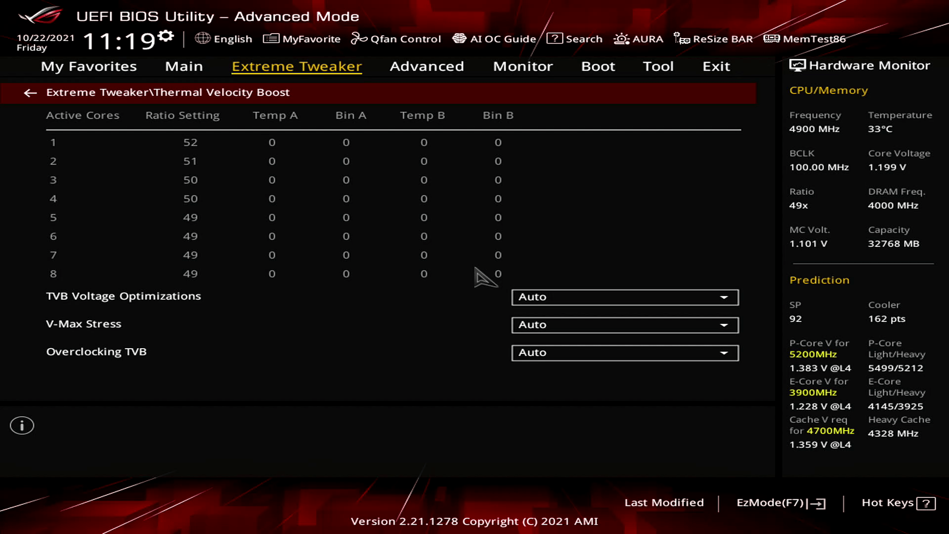
In the ASUS ROG BIOS, you can configure the by core usage ratios in the Extreme Tweaker menu. Just set Performance Core Ratio and Efficient core ratio to by core usage. This will reveal the by core usage configuration options.

Per Core Ratio Limit
First introduced on Rocket Lake and now inherited by Alder Lake, each CPU core has its own PLL.
PLL stands for phase-locked loop or phase lock loop. Simply put, the PLL generates an output signal such as clock frequency. Each core has its PLL means the processor cores can operate at independent frequencies. Before Rocket Lake, on mainstream desktop, all CPU cores of the CPU would run the same CPU ratio.
Alder Lake inherits this functionality from Rocket Lake and offers Per Core Ratio Limits for each of the P-cores and both clusters of 4 E-cores.

The Per Core Ratio Limit allows the bios to configure each physical core to its independent maximum boost ratio. This enables two important new avenues for CPU overclocking.
- First, it allows users to individually overclock each of the cores and find the maximum stable frequency.
- Second, it allows users to set an aggressive by core usage overclock while constraining the worst cores. This is particularly interesting considering Alder Lake CPUs have multiple favored cores and different types of cores. With Per Core Ratio Limit you can now prioritize one favored core to potentially run one ratio higher than the other core.
Note that while each of the CPU cores now has its independent PLL (and its independent V/F curve), still only one voltage is applied across all cores. The voltage applied is the highest of all active cores.
In the ASUS ROG BIOS, you can access the Per Core Ratio Limit options via the Extreme Tweaker Specific Performance Core and Specific Efficiency Core sub-menus. In this sub-menu, you can configure the ratio limit for each of the cores on your CPU.

Disable Ring to Core Ratio Offset
A standard feature of Intel CPUs since Kaby Lake, and of course inherited by Alder Lake, is a power management feature that reduces the Ring ratio by several steps compared to the Core ratio. In a typical situation, you would see the ring down bin of 3, meaning that if the CPU cores are running at 4.5GHz the system would configure the Ring ratio to 4.2 GHz.
While not technically an overclocking feature, Ring down-bin is an important feature to keep in mind when trying to achieve high performance. The CPU Ring is the bus that connects all different parts of the Intel CPU to transfer data between different cores, between cores and memory, and between cores and other parts of the system.
The Ring has its own voltage-frequency curve, meaning it will request a certain voltage when running a certain frequency. However, the CPU cores and Ring share the same voltage plane. So, if you force a specific Ring frequency that requires a higher voltage, is it very possible that would result in effectively overvolting the CPU cores. That in turn would increase the temperatures and power consumption.
The default ring frequency is significantly affected by E-cores. When only P-cores are enabled, the ring frequency is 4.7GHz. However, when E-cores are enabled (and active) the ring frequency drops to 3.6 GHz.
Disabling ring to core ratio offset is specifically important when manually overclocking as it ensures that your manually set ratio for the ring is always applied.
In the ASUS BIOS, you can change the Ring Down Bin settings in the Extreme Tweaker menu. By default, ring-down bin is enabled. If you want to force a specific ratio, you must disable the option and set a minimum CPU Cache Ratio.

AVX2 Negative Ratio Offset (Per Core)
Intel first introduced the AVX negative ratio offset on Broadwell-E processors. Successive processors adopted this feature and eventually expanded it with AVX2 and AVX-512 negative offsets.
AVX negative ratio offsets are very useful to achieve maximum performance for both SSE and AVX workloads. Generally speaking, an offset of 2 or 3 is recommended but it is highly dependent on not only your cooling solution but also the motherboard you’re using. That is because AVX workloads are very demanding and therefore require great cooling and power delivery.
While the function carried over in principle, there are some big differences in the implementation of AVX ratio offset between Alder Lake and Rocket Lake.
- First, on Alder Lake, the AVX2 negative ratio offset is only applied to the P-cores. The E-core frequency is unaffected.
- Second, by default, the maximum ratio during an AVX workload is the Turbo Boost 2.0 ratio. If you want an offset of 0, so AVX workload doesn’t reduce the frequency, you’ll need to manually set 0. Note that on some BIOSes programming 0 means programming “default”, in which case you’ll be limited to a maximum 51X for the AVX ratio on the 12900K.
- Just like on Rocket Lake, the AVX negative offset is referenced against each core as Alder Lake supports independent ratios for each P-core. Before Rocket Lake, the AVX offset would be referenced against the all-core maximum ratio. As the AVX offset will be applied to each core separately, you’ll have to be a little careful when your overclock has different ratios for different cores.
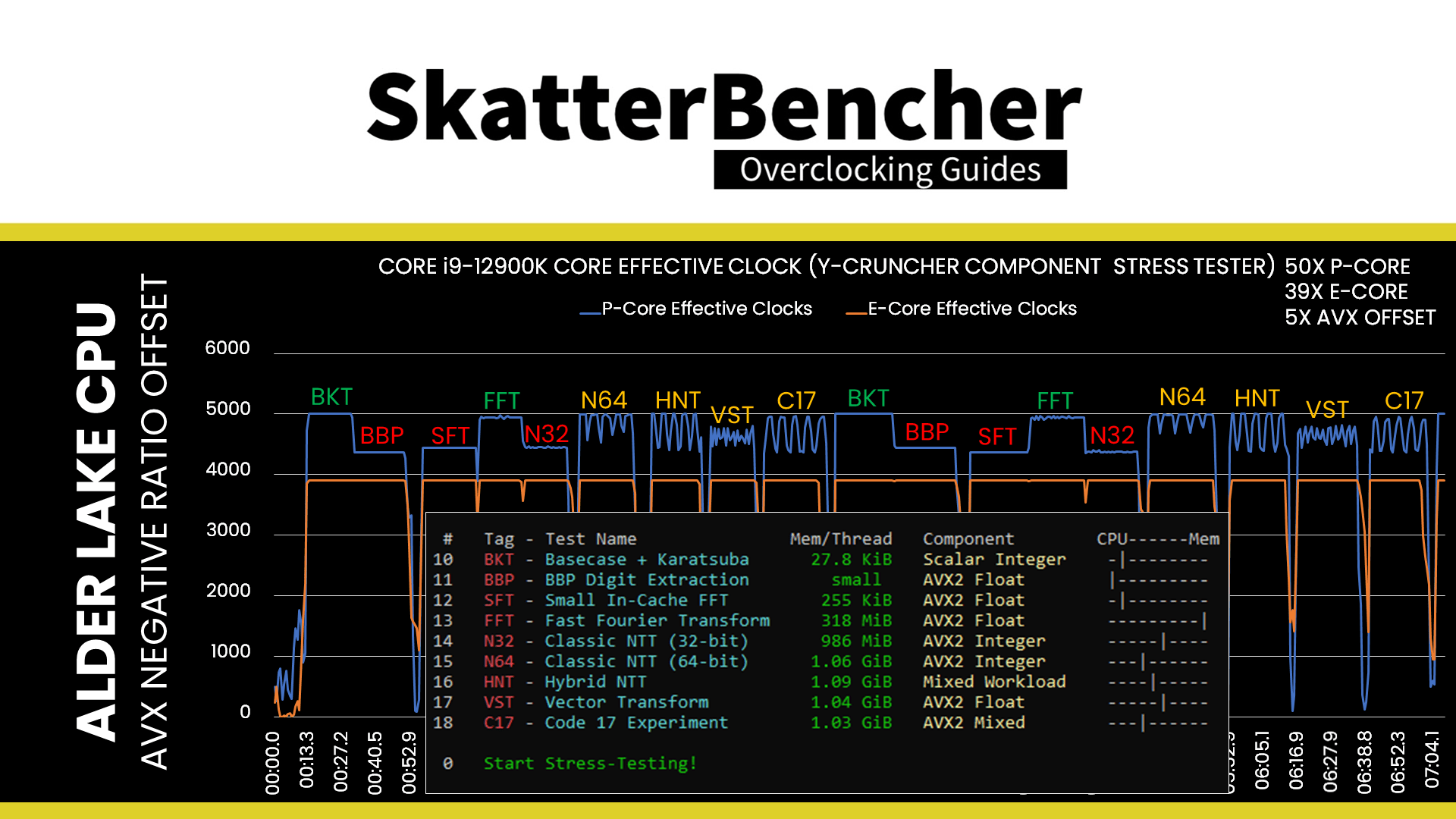
- Third, Intel has made some changes to how it flags an AVX workload. The effect is that some light AVX workloads will no longer trigger the AVX negative offset. We can demonstrate this new behavior using Y-cruncher.

Using Y-cruncher component stress tester, we run a variety of AVX workloads on the 12900K. We configure the 12900K as follows: 5GHz for the P-cores, 3.9GHz for the E-cores, and an AVX offset of 5 ratios. Then we use HWiNFO to monitor the effective clock during the benchmark
During the Y-cruncher workloads, we see that during BKT the P-core effective clock frequency is 5GHz. Since this is a non-AVX workload, it’s as expected. Then there are two AVX workloads, BPP and SFT, where the P-core effective clock drops to 4.5 GHz. This is expected as the 5 GHz P-core frequency is reduced by 500 MHz due to the AVX offset.
During the FFT workload, also AVX, the frequency is back to 5 GHz. So, the AVX offset was not triggered. Then the next 4 AVX workloads, N64, HNT, VST, and C17, bounce back and forth the AVX offset and non-offset.
In the ASUS BIOS, you can configure the AVX2 Negative Ratio Offset in the Extreme Tweaker AVX Related Controls sub-menu. First set AVX2 Ratio Offset to per-core Ratio Limit to User Specify, then configure the AVX2 Ratio Offset as desired.

AVX2 & AVX512 Enable & Disable
In addition to the ability to reduce the CPU frequency with the AVX ratios, an additional feature related to AVX is the ability to enable or disable AVX2 instructions. Disabling AVX causes the software to take non-AVX execution paths resulting in lower performance.
So, it doesn’t mean AVX-enabled software won’t run. It just means lower performance.
As I mentioned earlier in the video, AVX-512 is a bit of a tricky conversation. In certain technical documentation, you could find references to AVX-512 being available on the P-cores but not the E-cores. Later, however, the official communication was that AVX-512 would not be available on Alder Lake.
However, turns out it IS available though there’s a caveat. You’ll need a specific BIOS that supports enabling AVX-512 instructions and you’ll need to disable all E-cores.

In the ASUS BIOS, you can enable and disable the AVX2 and AVX-512 functions in the Extreme Tweaker AVX Related Controls sub-menu.

If you wish to disable the E-cores, in the ASUS BIOS you can do so in the Advanced CPU Configuration sub-menu. Simply set Active Efficiency Cores to 0.

AVX Voltage Guardband Scale Factor
Another feature that was first introduced on Rocket Lake and is inherited by Alder Lake is AVX Voltage Guardband Scale Factor.
Voltage guard-banding ensures that the effective voltage stays within the required range at all times to ensure stability. Users are given an option to change the voltage guard-band when running AVX2 instructions using the Voltage Guard-band Scale Factor.
The scale factor is a number between 0 and 2.0, where 0 means no scale factor is applied and 1 means the default scale factor is applied.
The resulting final guardband is as follows: AVX2 Final Voltage Guardband = AVX2 default guardband * AVX2 Scale Factor
Note that the value of the guard band is arbitrary and may vary from CPU to CPU. Also, it may be a very small value so adding any scale factor would not show any or limited results.
In the ASUS BIOS, you can configure the AVX Voltage Guardband Scale Factor in the Extreme Tweaker AVX Related Controls sub-menu.

Per-Core Hyper-threading
Alder Lake also supports non-uniform hyper-threading (HT) where some cores can have HT enabled and others have HT disabled. This feature is present since Comet Lake and while it maybe seemed an odd feature at the time, with Alder Lake the function is pretty self-evident.
While the P-cores have hyper-threading enabled, the E-cores do not. Therefore, Per-Core Hypert-hreading is only available for the P-cores.
One theoretical example where this could be useful is if you have a 20 threaded workload and you want to have exactly 20 threads enabled on a system with 12900K. In that case, you could opt for:
- 8 P-cores with HT enabled plus 4 E-cores = 8×2 + 4 = 20 threads
- 4 P-cores with HT enabled, 4 P-cores with HT disabled, and 8 E-cores = 4×2 + 4 + 8 = 20 threads
In the ASUS ROG BIOS you can configure the per core hyperthreading by going to the Advanced Menu, then enter the CPU Configuration sub-menu, then enter the Per Core Hyper-threading sub-menu.

Alder Lake Overclocking: Integrated Graphics
In this section, we will discuss the topics that relate specifically to overclocking the Intel Alder Lake integrated graphics.
Overview
As the term integrated graphics already reveals, the UHD Graphics 770 is integrated into the Alder Lake CPU die. While it takes a sizeable chunk of the total die the majority of the chip is used to place 8 Golden Cove CPU P-cores and 8 Gracemont CPU E-cores, its cache, and the Ring bus.
The design of the integrated graphics can be separated into three parts: the “slice”, the “unslice”, and the display block.
The slice is a cluster of sub-slices, each of which contains the elements of the actual graphics compute engine like the execution units. This is the part that powers your games and any compute tasks.
The unslice holds the elements with fixed-function geometry capabilities and fixed-function media capabilities. So, if you’re encoding or decoding a video, or simply watching Netflix, this part ensures proper video encoding. It also contains the connection to the ring bus via which the IGP can send and receive data from the system memory.
The display block contains support for the display outputs like HDMI or DisplayPort.
The slice part of the UHD Graphics 770 inside our desktop Alder Lake Core i9-12900K contains 2 sub-slices with each 16 execution units. That’s far less than the 6 sub-slices and 96 execution units present in the mobile Alder Lake parts.

When it comes to clocking, the IGP frequency is based on the base clock frequency or reference clock. By default, the BCLK is 100MHz, but it can be increased when overclocking. The base clock frequency is first halved, then multiplied by the Graphics Ratio to obtain the final operating frequency.
On Alder Lake CPUs, the maximum Graphics Ratio Limit is 42. This is the same as Rocket Lake but lower than on the previous generation Comet Lake where the maximum ratio limit was 60. I’m not sure why the maximum ratio has been reduced. You could say the maximum IGP frequency is 2100 MHz, but you can further increase the frequency by using BCLK overclocking. Spoiler alert: you may very well need BCLK to max out the IGP.

Just like on Rocket Lake, having separate Slice and Unslice frequencies is not supported. So, when increasing the graphics ratio, we will increase both the Slice and Unslice frequency. Do note that the display output is driven by a 24 MHz fixed clock frequency and is not affected by changing the BCLK frequency or the graphics ratio.
When it comes to providing an operating voltage to the graphics cores, the Alder Lake processor has a dedicated voltage rail called VccGT or GT Core Voltage. This voltage relates directly to the maximum frequency capability of the graphics cores. It is by default around 1.05V.
As mentioned before, the slice and unslice share the same voltage rail so their operating voltage will be the same.

Configuring the voltage for the graphics cores is very similar to the CPU cores. Alder Lake supports both adaptive and override voltages. When using Adaptive voltage mode, the graphics voltage will be reduced in idle whereas in Override voltage mode the voltage will remain constant.
Graphics Dynamic Frequency
The Alder Lake integrated graphics support the Graphics Dynamic Frequency feature. The Dynamic Frequency capability is designed to allow the processor to assess its thermals, current, and power to come up with a dynamic upper limit on its frequency.
On processors with Graphics Overclocking capability, the integrated graphics cores can run at frequencies higher when operating conditions allow.
When Graphics Dynamic Frequency is enabled, the graphics cores could be running at any ratio in the inclusive range between the Maximum Dynamic Frequency (RP0) and the Graphics Base Frequency (RP1). In the case of our Core i9-12900K, the graphics base frequency is 300 MHz, and the default maximum dynamic frequency is 1550 MHz. When overclocking, we simply increase this Maximum Dynamic Frequency (RP0) to a higher value.
As mentioned, the graphics frequency is in part a function of the available thermal, current, and power headroom. This is managed by the Turbo Boost 2.0 technology we are all too familiar with. Turbo Boost 2.0 will ensure the available power budget is distributed among the CPU and Graphics cores depending on the workload. So, if you have a heavy graphics-dependent workload and no CPU load, it will decrease the CPU frequency in favor of boosting the Graphics frequency higher.
Of course, knowing the power budget of the Graphics portion of the Alder Lake CPU is only 15W, we don’t expect this power budgeting to have a great impact on our overall system performance.
In the ASUS ROG BIOS, you can configure the Maximum Dynamic Frequency in the Extreme Tweaker menu. Change the ratio by configuring the Max. CPU Graphics Ratio in the Extreme Tweaker menu.

Adaptive Voltage Mode
As mentioned before, Alder Lake supports both adaptive and override voltages for the GT voltage rail. When using Adaptive voltage mode, the graphics voltage will be reduced in idle whereas in Override voltage mode the voltage will remain constant.
In adaptive mode, the CPU will interpolate the required voltage for a given frequency between the base frequency and our set maximum frequency.
Considering our base frequency is 300 MHz at 0.9V and our maximum boost frequency is 1550 MHz at 1.05V, then the interpolated voltage for 1000 MHz will be somewhere between 0.9V and 1.05V. If the V/f curve is linear, that would be 0.96V
When we overclock our system to 2.3GHz and use an adaptive voltage offset of 300mV, the base frequency will be 300 MHz at 1.2V and the maximum boost frequency will be 2300 MHz at 1.35V. The interpolated voltage for 1000 MHz will be somewhere between 1.2V and 1.35V. If the V/f curve is linear, that would be 1.26V.

In the ASUS ROG BIOS, you can configure the Maximum Dynamic Frequency in the Extreme Tweaker menu. You can change between Adaptive and Override mode by configuring the CPU Graphics Voltage option.

Alder Lake Overclocking: DDR4/DDR5 Memory & Memory Controller
In this section, we will discuss the topics that relate specifically to overclocking memory with Intel Alder Lake.
One of the biggest novelties with Alder Lake processors is of course DDR5! It’s the first platform that supports this new memory technology and PC enthusiasts are undoubtedly excited to see what it brings in terms of performance. While Alder Lake is primarily a platform for DDR5, the CPU also supports DDR4.
We won’t spend too much time covering the DDR4 overclocking intricacies as it’s very similar to Rocket Lake. However, let’s dig a little deeper into DDR5.
DDR5 Memory Overview
This article on rambus.com concisely lays out what are the major differences between DDR4 and DDR5. There are 6 key advantages of DDR5 versus DDR4
- Higher bandwidth: DDR5 enables clock rates of up to 3.2 GHz resulting in a data rate of 6.4 Gbps. This is double of what DDR4 is specified as, though of course the overclocking world record of DDR4 has already surpassed DDR4-6666.
- DDR5-4800 is the equivalent of DDR4-1600 base specification
- DDR5-6400 is the equivalent of DDR4-3200 maximum specification
- Lower power: the IO voltage has been reduced from 1.2V on DDR4 to 1.1V on DDR5
- SDR: 3.3 VDD
- DDR1: 2.5 VDD
- DDR2:
- DDR3: 1.8/1.35 VDD
- DDR4: 1.2 VDD / 2.5 VPP
- DDR5: 1.1 VDD / 1.8 VPP
- Better power efficiency: the power management has moved from the motherboard VR to the DIMM PMIC. PMIC stands for Power Management Integrated Circuit
- SDR: 576mW
- DDR1: 430mW
- DDR2:
- DDR3: 300mW
- DDR4: 184mW
- DDR5: -8-10% mW
- Higher memory efficiency and lower latency: DDR5 memory offers 2 40bit channels per DIMM whereas DDR4 offers only 1 72bit channel per DIMM
- Longer burst length: DDR4 burst chop length is four and burst length is eight. For DDR5, burst chop and burst length will be extended to eight and sixteen to increase burst payload. Burst length of sixteen (BL16), allows a single burst to access 64 Bytes of data, which is the typical CPU cache line size. It can do this using only one of the two independent channels.
- Higher capacity: the maximum die density has increased from 16Gb to 64Gb. So while a DDR4 module can have up to 64GB of memory, DDR5 modules increase this to 256GB.
- On-die ECC is available, though note that ECC must be supported by the memory controller
While the current DDR5 JEDEC specification lists up to DDR5-6400, it is expected this will further increase to DDR5-8400 and beyond in the future.
So, the main takeaway from DDR5 is that speed and capacity will go up while voltages go down. Also, the voltage is no longer provided by the motherboard voltage regulator but by the onboard PMIC.
DDR5 PMIC
PMIC stands for Power Management Integrated Circuit and its purpose is exactly what you think it is: provide power regulation for the memory module.
JEDEC, the organization responsible for developing open standards for microelectronics such as DDR5, outlines 5 motivations for moving the memory voltage regulation from the motherboard to the memory module:
- Power integrity and signal integrity concerns
- Cost reduction
- Form factor
- Voltage accuracy, and
- DRAM customization
On the Alder Lake desktop, the DDR5 PMIC has two input voltages: 5V and 3.3V. On server platforms, it looks like this may be 12V and 3.3V. The spec further defines 4 switching output regulators for 2 times VDD, VDDQ, and VPP, and 2 LDO outputs of 1.8V and 1.0V.
- VDD is 1.1V
- VDDQ is 1.1V
- VPP is 1.8V

The PMIC also has plenty of other features such as I2C and I3C, over-voltage and over-temperature protection, and so on.
As every DDR5 stick has its own PMIC, you can run separate voltages on the sticks. Fortunately, some if not all BIOSes will allow you to sync the voltage of your memory modules.
There are multiple PMIC vendors including Renesas, Richtek, and Anpec. Which vendor is the best for overclocking is hard to say as we’re still so early in the DDR5 lifecycle and, of course, there is a shortage of DDR5 ICs.
What is important to know for overclocking, however, is that there are two types of PMICs: secure and non-secure.
The main difference is that secure PMICs support voltages up to 1.435V in steps of 5mV and non-secure PMICs support voltages up to 2.070V in steps of 10mV. This granularity is important for extreme overclockers who are looking to push the memory frequency to the limit.

For daily overclocking the upper limit of 1.435V will be sufficient. Also, note that it looks like motherboard vendors have already found a way to “unlock” secure PMICs … so there’s that.
In the ASUS ROG BIOS, you can access the PMIC settings in the Extreme Tweaker Advanced Memory Voltages submenu. You can change the settings of all PMIC in sync or change the settings of each PMIC individually.

DDR5 ICs
At launch, there will be DDR5 ICs available from 3 manufacturers: Micron, Hynix, and Samsung.
The overclocking capabilities of each of the ICs are still a big unknown. Generally, it looks like Micron is the worst of the thread, then Hynix and Samsung are somewhat on par with Hynix maybe having the edge in overall performance (frequency and timings).
This won’t matter much at launch, however, as there will be a severe shortage of DDR5 in the market. From the looks of it, Micron will have the most availability through their subsidiary Crucial.

In terms of XMP-rated kits, I believe we’ll see north of DDR5-6000 available in limited quantity as this kind of speed requires Hynix or Samsung ICs.
In terms of overclocking guidance, there’s not much information I can provide. Shamino from ASUS ROG did put together a great table based on his findings, so I’ll leave you with that.

Intel Extreme Memory Profile 2.0
Intel Extreme Memory Profile, or XMP, is an Intel technology that lets you automatically overclock the system memory to improve system performance.
Intel XMP is an extension to the standard JEDEC specification that allows a memory vendor to program different settings onto the memory stick. The settings include the memory frequency, the memory timings as well as the memory voltage.
The Intel XMP standard uses this extension for overclocking purposes and adds a couple of features to the memory standard:
- Multiple SPD profiles – This allows for several different memory profiles which can be selected depending on the usage; for example for a special low-latency custom profile for gaming.
- Memory vendor-specific SPD fields – This gives memory module suppliers the ability to set a number of their own profiles based on the module capabilities.
- Easy Over-clocking (Novice) – Provides users with several predefined overclocked profiles that have been determined to be stable. This allows users to select those predefined profiles instead of adjusting individual parameters in BIOS.
- Advanced Overclocking (Intermediate/Expert Users) – Allows more advanced users to change specific SPD parameters in the BIOS and save those profiles.
- Fail-safe default boot – Allows the ability to restore to one of the usual default JEDEC settings after a bad configuration
There are two types of XMP certification:
- XMP ready: the module is programmed with an uncertain, but stable, profile
- XMP Certified: the module is programmed with settings that have passed supplier tests for the CPU and motherboard.
You can find the list of XMP Certified products on Intel’s website.
Intel XMP 1.0 was developed for DDR3 and was later superseded by XMP 2.0 for DDR4. With the launch of DDR5 memory, there is now an XMP 3.0 too. As Alder Lake CPUs supports both DDR4 and DDR5, it also supports Intel XMP 2.0 and Intel XMP 3.0 technology.
Before we jump into XMP 3.0, if you want to know which XMP profiles your memory supports, there are several ways to do it.
- First, if your memory is rated above DDR4-3200, it almost definitely has an XMP profile. That is because the JEDEC standard only goes up to DDR4-3200.
- Second, you can look in your BIOS and find the option to enable XMP. Most, if not all, motherboards support XMP and even allow you to check the specific configuration in BIOS.
- Third, you can use CPU-Z and check the SPD tab. Here you will find the basic XMP profile settings in the Timings Table section.
I almost always run XMP on my systems because it is an incredibly easy and safe way to improve system performance. Do note that some motherboards may adjust CPU memory controller voltages to support extremely high-frequency memory.
In the ASUS ROG BIOS, you can enable XMP in the Extreme Tweaker menu. First set Ai Overclock Tuner to XMP I or XMP II. Then select the XMP profile in the XMP section.
XMP I will only load the primary timings of the XMP profile and will leave the rest of the optimization to the motherboard auto-rules and optimizations. XMP II will load the complete XMP profile and disregard any auto-rules from the motherboard.

Intel Extreme Memory Profile 3.0
Intel Extreme Memory Profile 3.0 is the new XMP standard for DDR5 memory. It is largely based on the XMP 2.0 standard but has additional functionality.
The XMP 3.0 standard is designed with six sections. One global section describes the generic data which is used across the profiles. The other five sections are designed for five profiles respectively.
- Profile 1 is meant for the performance profile (this is the standard XMP as we know it)
- Profile 2 is designed for the extreme settings (this could be a higher frequency at higher voltage)
- Profile 3 is designed for the fastest settings (this could be tighter timings at higher voltage)
- Profiles 4 and 5 are rewritable and meant for user custom settings

The Global Section has only a few configurable fields:
- The XMP ID string
- The XMP version (this will be 3.0 for DDR5)
- The XMP organization (this allows memory vendors to enable or disable Profiles 2 and 3. Profiles 4 and 5 are always enabled)
- The XMP recommended channel configuration (each profile can have a 1 to 4 DIMM per channel recommendation)
- PMIC Vendor ID
- Number of PMICs
- PMIC capabilities
- OC functions available Y/N:
- When set to No, the PMIC supports only the JEDEC specification on frequency and voltage.
- When set to Yes, the PMIC supports additional capabilities of Intel XMP requirements and overclocking capabilities which are out of JEDEC spec. Intel XMP requirements include “programmable” mode and the voltages support higher than 1.435V with 5/10mV switches.
- OC functions enabled Y/N
- This is by default set to enabled when the PMIC supports OC function
- PMIC voltage step size: 5mV or 10mV
Each profile has a wide range of configurable fields related to voltage, frequency, and memory timings, including:
- Module VPP
- Module VDD
- Module VDDQ
- Memory Controller Voltage Level
- tCL
- tRCD
- tRP
- tRAS
- tRC
- tWR
- tRFC1
- tRFC2
- tRFCsb
- Dynamic Memory Boost support
- Real-Time Memory Frequency OC support
- Command Rate
- Vendor ID
The main takeaway from XMP 3.0 is the following:
- It offers more profiles including 2 which are rewriteable by the user to save custom settings
- It offers extended functions to distinguish between OC and non-OC memory sticks, where non-OC follows JEDEC and OC allows for extended voltage, current, and frequencies.
- The memory profile now includes also a voltage for the CPU memory controller
In the ASUS ROG BIOS, you can enable XMP in the Extreme Tweaker menu. First set Ai Overclock Tuner to XMP I or XMP II. Then select the XMP profile in the XMP section.
XMP I will only load the primary timings of the XMP profile and will leave the rest of the optimization to the motherboard auto-rules and optimizations. XMP II will load the complete XMP profile and disregard any auto-rules from the motherboard.

Alder Lake Memory Controller Overview
As mentioned before the Alder Lake CPU has 2 memory controllers. On a typical 4 DIMM motherboard, the memory slots are organized as follows. From left to right:
- MC0 D0 (Memory Controller0, Dimm0): Slot1
- MC0 D1(Memory Controller0, Dimm1: Slot2
- MC1 D0 (Memory Controller1 Dimm0): Slot3
- MC1 D1(Memory Controller1 Dimm1: Slot4

Depending on your definition of what constitutes a memory channel, we’ll talk about dual-channel or quad-channel support on Alder Lake with DDR5. DDR5 features two independent 32-bit memory channels per module, versus a single 64-bot channel on DDR4.
So, assuming we consider a DDR5 module a “dual channel” module, we can consider the following configuration.
- If you run DDR4 memory and have a stick in only Slot 1, then you will run 1 memory controller with a single channel enabled. So single channel.
- If you run DDR4 memory and have a stick in Slot 1 and Slot 2, then you will run 1 memory controller with a single channel enabled. So single channel.
- If you run DDR4 memory and have a stick in Slot 1 and Slot 3, then you will run 2 memory controllers with single-channel enabled. So dual channel.
- If you run DDR5 memory and have a stick in only Slot 1, then you will run 1 memory controller with dual-channel enabled. So dual channel.
- If you run DDR5 memory and have a stick in Slot 1 and Slot 2, then you will run 1 memory controller with a dual-channel enabled. So dual channel.
- If you run DDR5 memory and have a stick in Slot 1 and Slot 3, then you will run 2 memory controllers with dual-channel enabled. So quad channel.

The default memory controller frequency will also be different for DDR4 and DDR5.
With DDR4 memory, the default memory controller frequency is the same as the memory frequency. So, at DDR4-3200 the memory frequency is 1600 MHz so the memory controller frequency will also be 1600 MHz.
With DDR5 memory, the default memory controller frequency is half of the memory frequency. So, at DDR5-4800 the memory frequency is 2400 MHz so the memory controller frequency will be 1200 MHz.
You can change the memory controller frequency either by altering the BCLK frequency or by changing the Gear mode.
For Gear Mode, it’s important to clarify two distinct “gear” terminologies.
- “Gear-down” is a JEDEC DRAM specification where the DRAM assumes the memory controller frequency is half of the memory frequency. We will discuss this a little later in the video.
- “Gear Type” is an Intel term used to describe the relationship between the memory controller frequency and the memory frequency.
- Gear 1 means the memory controller frequency is the same as the memory frequency
- Gear 2 means the memory controller frequency is half the memory frequency
- Gear 4 means the memory controller frequency is a quarter of the memory frequency
As a consequence, the DRAM ratio must match with the Gear. Gear 2 requires the DRAM ratio to be divisible by 2, and Gear 4 requires the DRAM ratio to be divisible by 4. For example:

The default specification for DDR4 is Gear 1 up to DDR4-3200. The official specification for DDR5 is Gear 2 up to DDR5-4800 for 1 module and Gear 2 up to DDR5-4000 for 2 modules.
All of the above is in theory since practically it seems only Gear 1 and 2 are functional for DDR4 and Gear 2 and 4 are functional for DDR5. The challenges are not only related to the memory controller – DDR5-4800 Gear 1 would have the memory controller run at 2.4 GHz – but also general auto-rule tuning of memory timings. I assume we will see improved compatibility for the various gears in the weeks and months after the Alder Lake launch.
In the ASUS ROG BIOS, you can select the Memory Gear Ratio in the Extreme Tweaker menu under the Memory Controller : DRAM Frequency Ratio option.

Memory Frequency
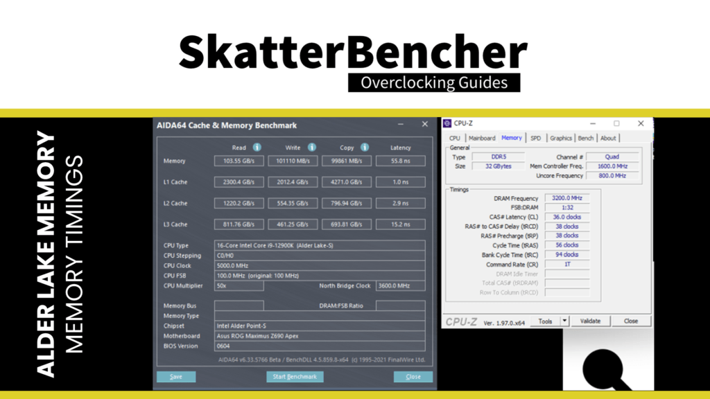
The memory frequency is driven by the memory controller and supports both 100 MHz and 133 MHz reference frequencies. The highest supported memory ratio is 63X, thus the maximum supported memory frequency by ratio is 133 MHz multiplied by 63 equals 8400 MHz or DDR5-16800.

In addition to the memory ratio, there is a function called Unlimited Qclk Frequency which allows for an unlimited frequency request up to a theoretical 34GT/s, or DDR5-34000, in Gear 1 mode. This is of course not super relevant to our daily overclocking system. Let’s just say there’s more than enough headroom.
In the ASUS ROG BIOS, you can select the memory frequency reference clock in the Extreme Tweaker menu under the BCLK Frequency: DRAM Frequency Ratio option

In the ASUS ROG BIOS, you can set the memory frequency in the same menu under the DRAM Frequency option.

Memory Gear-Down Mode
First introduced on Rocket Lake and now also available on Alder Lake is the option to operate the memory in gear-down mode.
Gear-down mode is a JEDEC DRAM specification where the DRAM assumes the memory controller is sending command/address signals at half the usual rate. Normally, the DRAM expects a command/address signal every clock cycle. In gear-down mode that becomes every other clock cycle. This comes of course with a performance penalty. To understand why there’s a performance penalty, we need to touch a little on how memory works.
On DDR5 memory, there are two buses. There’s one command/address bus and one data bus.
As the name already explains, when the CPU wants to read or write data to the memory, it uses a command and address to specify what needs to be done and where. The actual data is sent over the data bus.
- The data bus is DDR, or double data rate, meaning it can send 2 signals per memory clock cycle. It does this on both the rising and the falling edge of the clock cycle.
- The Command/Address bus is SDR, meaning it can process 1 signal per memory clock cycle. It does this on the rising edge of the memory clock cycle.

Now with DDR5 things are a little different than with DDR4. So, let’s first review how gear-down mode worked on DDR4.
As the command/address bus is the main communication bridge between the memory controller and the system memory, their operating frequencies are usually synchronized. That means the memory controller and memory operate at the same frequency.
In normal operation with DDR4, every clock cycle there is 1 command/address signal sent from the memory controller to the memory. And, the memory also expects 1 signal per clock cycle. So, everything works fine.

When gear-down is enabled, that’s not the case. In gear-down mode the memory expects a command/address signal every other clock cycle. A convenient or even necessary consequence of using the command/address bus every other clock is that you can run the memory controller at half the frequency and still achieve the same performance.

Let’s look at an example with DDR4 memory.
As you can see from the table above, the default operation for DDR4 is to have the memory controller and memory frequency run at the same frequency with gear-down mode disabled.
When gear-down mode is enabled the DRAM expects half the amount of command/address signals. This opens the opportunity to reduce the memory controller frequency by half.
This is the implementation we saw on Rocket Lake and the reduced memory controller frequency vis-à-vis the memory controller is the main reason behind its the increased memory overclocking capabilities.

Now, DDR5.
A major selling of DDR5 is its promised much higher operating frequencies. Leading up to the Alder Lake launch we already saw leaks of DDR5-8000 and more. For your information, the highest DDR4 memory frequency to date is a measly DDR4-7200.
To support these higher operating frequencies, the default configuration for Alder Lake is to operate the memory controller at half the frequency of the system memory. However, it now sends 2 command/address signals per memory controller clock cycle. So, from the DRAM perspective, for each DRAM clock cycle, there will still be 1 command/address signal.

Let’s expand our table from before.
Again, as you can see from the table above, the default operation for DDR5 is to have the memory controller run at half the memory frequency with gear-down mode disabled. Because the Alder Lake memory controller sends 2 command/address signals per memory controller clock cycle, from the memory’s point of view there is still 1 command/address signal received per memory clock cycle.
When gear-down mode is enabled the Alder Lake DDR5 memory controller runs at a quarter of the memory frequency.

So, let’s re-iterate.
For Alder Lake and DDR5 memory, the standard configuration is that the Alder Lake memory controller sends 2 command/address signals every memory controller clock cycle. The memory controller frequency operates at half the DDR5 memory frequency. So, the effective amount of command/address signals processed by the DDR5 memory is still 1 every memory clock cycle.
Memory gear-down mode specifically means that a command/address signal is sent every other memory clock cycle. This allows us to operate the memory controller frequency at half the usual rate. For Alder Lake and DDR5, that means when gear-down mode is enabled the memory controller will operate at a quarter of the memory frequency.
Note that from the perspective of the memory controller, a command is sent every clock cycle.
At the end of the day, the point of gear-down mode and gear types is that you can run higher memory frequency by reducing the memory controller frequency. What’s possible in theory isn’t necessarily useful in practice. So, let me leave it at this:
- For low-to-medium frequency DDR4, run normal mode with 1T and the memory controller frequency identical to the DRAM frequency
- For high-to-extreme-frequency DDR4, run gear-down mode with 2T and the memory controller at half the DRAM frequency
- For regular frequency DDR5, run gear-down disabled with 1T and the memory controller at half the DRAM frequency
- For extreme-frequency DDR5, run gear-down enabled with 2T and the memory controller at a quarter of the DRAM frequency

In the ASUS ROG BIOS, you can select the Memory Gear Ratio in the Extreme Tweaker menu under the Memory Controller : DRAM Frequency Ratio option.

Memory Timing Overrides
Of course, Alder Lake also supports overriding the memory timings as it’s crucial for improving memory performance. The memory timing support for DDR4 and DDR5 are identical. The full list of supported memory timings are:
- CAS Latency (tCL)
- Requires use of even numbers, odd numbers don’t work
- RAS to CAS Delay (tRCD)
- Row Precharge Time (tRP)
- Row Active Time (tRAS)
- Write Recovery Time (tWR)
- Minimum Refresh Recovery Time (tRFC)
- System Command Rate Mode (NMode)
- Read to Precharge delay (tRTP)
- Row Cycle Time (tRC)
- Four Active Window Delay (tFAW)
- Average Periodic Refresh Interval (tREFI)
- Minimum CAS Write Latency Time (tCWL)
- Requires use of even numbers, odd numbers don’t work
- Row Active to Row Active delay short and long (tRRD_S and tRRD_L)
- Internal Write to Read Command Delay short and long (tWTR_S and tWTR_L)
Broadly speaking, tuning the memory timings on DDR5 is very similar to DDR4. The timings themselves haven’t changed so any knowledge you have from DDR4 is useful for DDR5 tuning as well.
Most people will be put off by the high primary timings on DDR5 though. Note that the lowest Cas Latency supported by DDR5 is 20. Lower values could possibly to set in the BIOS, however values lower than 20 can simply not be programmed on the DDR5 module. Also, both Cas Latency and Write Latency values must be even by design.
While it may seem natural to first look at lowering the primary timings to obtain more memory performance, on DDR5 it looks like most performance is to be gained from tuning the tertiary sub-timings.

The DDR5 memory bandwidth at JEDEC specification of DDR5-4800 C40 is around 70 GB/s with a latency of 105ns. However, as demonstrated by ElmorLabs testing, XMP or pre-defined ASUS memory profiles allow you to achieve up to 100 GB/s read bandwidth and a latency below 55ns.
In the ASUS ROG BIOS, you can access the memory timings in the Extreme Tweaker DRAM Timing Control sub-menu.

Alder Lake Overclocking: Other Topics
In this section, we will cover overclocking-related topics that didn’t fit the other categories.
BCLK Aware Adaptive Voltage
BCLK Aware Adaptive Voltage was introduced along with the Kaby Lake processors back in 2016.
To understand its function, you can refer to the Adaptive Voltage Mode explanation from earlier. Whereas the Adaptive Voltage is designed to work with only the CPU ratios, when enabling BCLK Aware Adaptive Voltage, the processor scales its voltage calculations for all the V/f power domains and produces a voltage based on frequency as opposed to the multiplier. The V/f power domains include the CPU cores, the Ring, and the integrated graphics.
In the ASUS BIOS, you can enable or disable the BCLK Aware Adaptive Voltage in the Extreme Tweaker menu. By default, this option is enabled and I would strongly suggest keeping this voltage enabled when using adaptive voltage mode and playing with the base clock frequency.

BCLK Governor
As everyone knows, Intel only allows BCLK Overclocking on overclocking enabled parts only. This includes the K CPUs and their variants like KF, KS, and KB, X CPUs, HK, and HQ mobile CPUs.
Just like on previous platforms, Alder Lake includes a circuit called BCLK Governor that calculates BCLK and issues a machine check error if BCLK is found to be higher than the allowed limit.
BCLK calculation does not rely on using the Integrated Clock Controller (ICC) from the PCH. It works with external clocks as well.
The BCLK Governor has been present on Intel CPUs since Skylake. In the past, there have been ways to hack the BCLK governor and enable BCLK overclocking on non-K SKU CPUs. There are rumors there was such a hack in early Alder Lake microcode, but this should have been patched by now.
Obviously, there is no option in the BIOS to enable or disable the BCLK Governor
TjMax Offset
TjMax is short for Temperature Junction Max.
Tjunction max is the maximum thermal junction temperature that a processor will allow before using internal thermal control mechanisms to reduce power and limit temperature. Activation of the processor’s thermal control system may cause performance loss as the processor typically reduces frequency and power to prevent overheating.
Many third-party utilities like HWiNFO can monitor the digital thermal sensor (DTS) on the processor die to see how close the system is approaching the TjMax without any destructive testing.
The TjMax for Alder Lake CPUs is the same as Rocket Lake CPUs: 100 degrees Celsius. TjMax Offset allows raising TjMax above the default (usually 100ºC) up to 115ºC.
In the ASUS BIOS, you can change the TjMax in the Extreme Tweaker Internal CPU Power Management submenu. You can set the Maximum CPU Core Temperature to up to 115C, though it is recommended only in situations where you want to explicitly push the system to its limit and not for daily operation.

PVD Ratio Threshold
First introduced on Rocket Lake platforms, the option to change the PVD ratio threshold is a bit of a complicated one. Essentially, it boils down to this.
Every phase-locked loop, or PLL, design has a minimum and maximum oscillation frequency. To generate a specific frequency, the PLL’s digitally controlled oscillator, or DCO, uses post-divider ratios of 1, 2, 4, or 8 to go from an incoming frequency to the right outgoing frequency.
The PVD Ratio Threshold is the ratio trigger that will make the DCO change the post-divider from 1 to 2, to 4, or 8. By default, on Alder Lake, the PVD ratio threshold to switch to an x2 post-divider is 15.
Here’s how it works for the CPU Core PLL:
- The BCLK is first generated from the external crystal or an external clock generator
- This is multiplied by the CPU Core ratio
- Based on the chosen CPU ratio, the DCO will use a specific post-divider
- Lastly, the DCO outputs the final frequency to the CPU core

For example, let’s say we use a BCLK of 100 MHz and choose a CPU ratio of 45X to achieve a 4.5 GHz CPU frequency. In that case,
- BCLK = 100MHz
- Ratio = 45 -> this is higher than the PVD ratio threshold of 15, so post-divider will be 1X
- Post-divider = 1
- DCO = 100 x 45 x 1 = 4500 MHz

Now, let’s say we use a BCLK of 300 MHz and choose a CPU ratio of 15X to achieve a 4.5 GHz CPU frequency.
- BCLK = 300MHz
- Ratio = 15 -> this triggers the x2 post-divider!
- PD = 2
- DCO = 300 x 15 x 2 = 9000 MHz -> out of range!

The Change PVD Ratio Threshold option allows us to change the threshold to switch to the x2 post-divider. This can help prevent out-of-range DCO frequency when greatly increasing the BCLK frequency.
In the ASUS BIOS, you can configure the PVD Ratio Threshold in the Extreme Tweaker Tweaker’s Paradise submenu.

Current Excursion Protection
New on Alder Lake is a feature called CEP or Current Excursion Protection. It appears to work similarly to the VIN Tracker on Asus X299 boards as enabling it reduces the current draw and temperatures by “phantom throttling”
However, the analogy is as per observation and thus non-technical. The actual way it works is unknown at the moment.
In the ASUS BIOS, you can enable the Current Excursion Protection option in the Extreme Tweaker Internal CPU Power Management sub-menu: IA CEP Enable or SA CEP Enable options.

FLL OC Mode
FLL stands for Frequency Locked Loop. I’m not an electrical engineer, so I won’t be able to explain how it works from a technical perspective. Therefore, let me just focus on the practical stuff.
Leading up to the Alder Lake product launch there were some issues with extreme overclocking. This is not uncommon as pretty much every platform requires less or more work to enable extreme overclocking. One of the issues that popped up was a PLL-related bug that caused the CPU frequency to report much higher frequencies than it was actually running. Even much higher than 10 GHz!
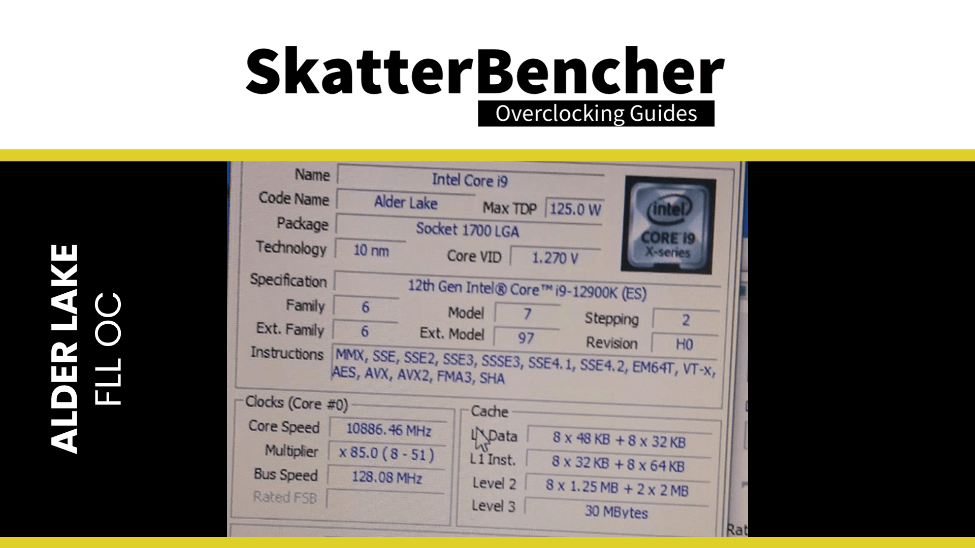
The FLL OC option fixes this specific issue with extreme overclocking.
For extreme overclocking aficionados who look forward to the maximum CPU frequency on Alder Lake, I believe CPU-Z should already have the FLL OC mode check in place to ensure the overclocking records validated on the website show the correct frequency. This should be the case from CPU-Z v1.98.
In the ASUS BIOS, you can access the FLL OC mode option in the Extreme Tweaker Tweaker’s Paradise sub-menu. I believe only “normal” has officially been validated. Either way, this is only useful for extreme overclocking.
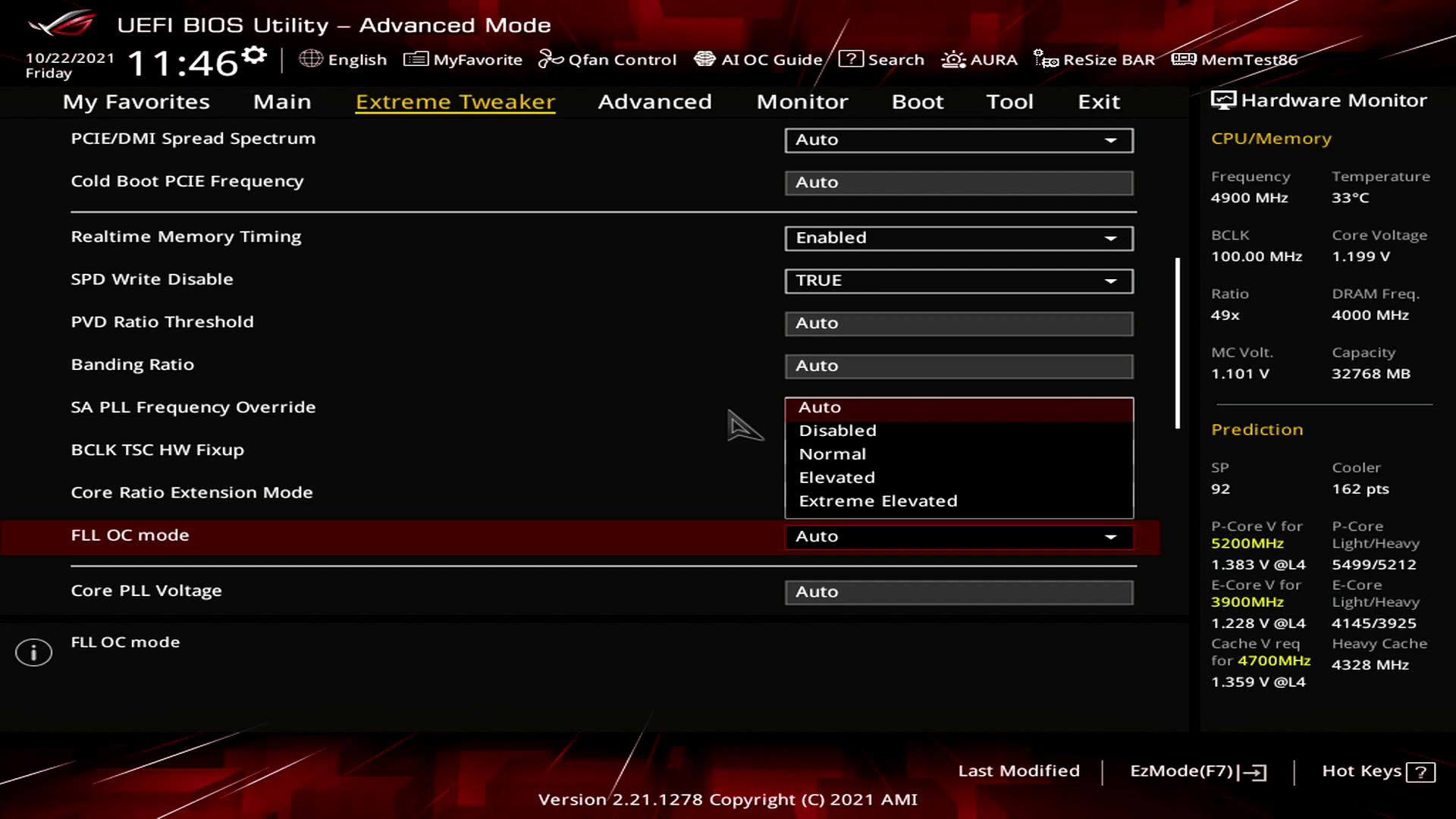
ASUS ROG Maximus Z690 Extreme Overclocking Technologies
In this section we cover the overclocking technologies and features present on the ASUS ROG Maximus Z690 Extreme motherboard.
ASUS AI Overclocking
For many years board vendors have tried to implement automatic overclocking features in their BIOS for simpler performance enhancement. This has always been a mixed bag as most of the preset OC profiles are overly optimistic in frequency target or overly generous with the voltage selection. So often you would end up with a slightly unstable or overheating system.
ASUS AI overclocking uses a different strategy. Instead of working with preset profiles, the system will monitor the CPU and cooling system throughout an initial phase of testing, then based on its findings predict the optimal settings. The system will then automatically guide the overclocking process and adjust voltages and frequency to match your cooling system.
The better your cooling, the higher your AI overclock.

There are three steps to enabling AI overclocking. First, reset the BIOS to default settings. Then, reboot and enter the operating system. Run a couple of heavy workloads such as Cinebench R23, Realbench, or Intel XTU for 10 to 30 minutes. Then return to the BIOS and enter the AI OC Guide menu from the top. Make sure to read through the explanation and when ready simply click Enable AI.
In the ASUS BIOS, you can access the AI OC Guide at the top of the BIOS or by pressing F11. You can also access the detailed AI Overclocking configuration settings in the Extreme Tweakers AI Features sub-menu. Also, you can select AI Optimized setting for the Performance Core Ratio and Efficient Core Ratio in the Extreme Tweaker menu.
I’ve used ASUS AI Overclocking in previous SkatterBencher articles, you want to learn how to use it you can check out those. I may revisit the AI Overclocking feature in more detail in the future.
ASUS MultiCore Enhancement
ASUS MultiCore Enhancement is a single BIOS option that removes all limits constraining the Turbo Boost 2.0 algorithm. Effectively, it allows the CPU to run at maximum turbo boost frequencies indefinitely. On Z690 motherboards, ASUS has enabled this option by default.

A major difference with the performance impact of MCE on Alder Lake versus the previous Intel generations is that Intel by default is very generous with the maximum power for Alder Lake.
Whereas in previous generations, the sustained power limit was always set to the specified TDP. So that’s 125W for K-SKU CPUs. MCE would enable the power limit to run at maximum, so by enabling it you’d get 280W to 300W of sustained power consumption (when you have sufficient cooling of course).
As mentioned before, for Alder Lake K CPUs the sustained power limit has been set higher than TDP. For the 12900K it’s 241W, for the 12700K it’s 190W, and for the 12600K, it’s 150W. Unlocking the power with MCE will therefore yield less of a performance increase over default as the 12900K CPU package power with MCE unlocked is around 300W in all-core AVX2 workloads.
In the ASUS BIOS, you can enable or disable ASUS MultiCore Enhancement in the Extreme Tweaker menu.
Package Temperature Threshold
I briefly covered this feature in the Rocket Lake launch video as well as SkatterBencher #25 with the Core i9-11900K.
In essence, this feature allows you to configure a maximum temperature for the CPU. The ASUS motherboard will track the CPU temperature during operation and once the temperature exceeds your target temperature, the CPU frequency will be reduced. It does this not directly by adjusting the CPU ratio, but rather by adjusting the Turbo Boost power limit parameters. By lowering the power limits, the Intel CPU will adjust the CPU ratio down on its own.

By default, ASUS has disabled this setting on the Z690 motherboards. It is enabled when you use AI Overclocking and then the package temperature threshold will be set to 90C.
In the ASUS ROG BIOS, you can adjust the package temperature threshold in the Extreme Tweaker AI Features submenu. Alternatively, you can also configure it in the Extreme Tweaker Internal CPU Power Management sub-menu.
To enable the feature, first set Regulate Frequency by above Threshold to enabled, then set the temperature threshold in the Package Temperature Threshold field.
ASUS Voltage Suspension
Voltage Suspension is a new feature that was launched with the Crosshair VIII Extreme motherboard. It is now also available for all Maximus Z690 motherboards. Voltage Suspension is a feature included in the External Digi+ Power Control menu of the BIOS.
The term suspension is akin to the suspension of a car, though I prefer the more technical term V-Clamp. The purpose of the V-Clamp is to force the Core Voltage to stay within a specific range even when using a dynamic voltage like with Precision Boost Overdrive.
To achieve this, there’s special hardware circuitry on the motherboard PCB. Essentially the circuitry has two main functions: one function to monitor what the CPU requests as VID (so voltage), another function to correct this request and adjust it according to our custom suspension rules.

We can configure the Voltage Suspension by setting the voltage ceiling and voltage floor. The ceiling is our maximum voltage and the floor is our minimum voltage. We can configure the ceiling and floor in static mode or dynamic mode.
In Static mode, we set a maximum and minimum voltage and the Voltage Suspension function will try to keep the voltage between these two levels.
In Dynamic mode, we kind of design our own voltage-frequency curve, though we don’t use frequency as a parameter directly. Instead, we configure the ceiling and floor voltage as the function of four points defined by a voltage and temperature. So, it’s more like a voltage temperature curve than a V/f curve.

In the ASUS ROG BIOS, you can configure the Voltage Suspension in the Extreme Tweaker DIGI+ VRM sub-menu. First enable the Core Voltage Suspension option, then select either static or dynamic mode for the ceiling voltage and the floor voltage.
I’ve used the voltage suspension feature in SkatterBencher #29 with the ASUS ROG Crosshair VIII Extreme. You can check out that article– or the dedicated page – if you want more information. As it was quite a useful feature to achieve a higher all-core overclock, I am planning to check it out with Alder Lake as well in a future video.
ASUS VLatch
VLatch was a brand-new feature on previous generation ROG motherboards that allow enthusiasts to detect the true Vmin and Vmax of the CPU core voltage without having to purchase an expensive oscilloscope. It is available on both the Maximus Z690 Apex and Extreme motherboard.
Explaining the VLatch function and purpose gets complicated very quickly but I’ll try to keep it as simple as possible.
In one of my previous videos, I talked about Intel Adaptive Voltage mode. In that video, I showed this drawing to explain how the CPU and motherboard VRM interact to provide a certain voltage. There are 3 basic steps:
- The motherboard communicates about its board design to the CPU via the ACDC Loadline
- The CPU requests a certain voltage by using a VID which is a combination of the factory-defined V/f curve and the ACDC loadline
- The voltage provided by the motherboard VRM is the requested voltage minus adjusted by the VRM loadline.
It’s the VRM loadline that many enthusiasts wish to have control over when trying to find the maximum stable settings.

Two parts of the loadline are important to system stability.
- First, the Vdroop. This is the decrease in voltage when the CPU goes from idle to load. You want your CPU to be stable in all scenarios so knowing what’s the lowest voltage the CPU will run at is very important. After all, if the voltage is too low then the overclock will be unstable.
- Second, the Undershoot and Overshoot. These are very brief spikes that occur when the CPU switches from idle to load, or from load to idle. These spikes cannot be measured easily and usually require an expensive oscilloscope to detect. I can highly recommend the ElmorLabs article titled VRM Load-Line Visualized if you want to see a great picture of undershoot and overshoot in action.

While undershoot and overshoot are very temporary spikes, an undershoot that’s too low will also cause instability.
With VLatch you can now detect the undershoot and overshoot. On the Maximus Z690 Extreme and Maximus Z690 Apex there’s a proprietary circuit design that allows the embedded controller to capture and report the true Vmin and Vmax.
You can use either HWinfo or the OLED display to see these voltages
I explored how to use VLatch in another article on this blog. Since the function is not different from the Z590 implementation, I would suggest you check out that video for a more detailed explanation.
ASUS ROG True Volticion
ROG True Volticion is a new physical accessory included with the Maximus Z690 Apex and Extreme. Volticion is a combination of voltage and optician. As you can already guess, it’s a tool to observe the voltages of your system
The Volticion is a USB oscilloscope. You can use it either on your system directly, or connect it via USB to a second system. The two options require a slightly different setup.
If you want to use the Volticion on the same system you’ll be checking the voltage of, simply plug the device in an available USB header on the motherboard. Then connect the 3 channel inputs to the OSC Sense pin headers on the motherboard. The pins on the motherboard, from left to right, are for Vcore, VCCIN, and VccSA.

If you want to connect the Volticion to a second system, then you need to use the micro-USB cable as well as connect the Ground pin to any ground on the motherboard. For example, using one of the FAN headers.
Remote monitoring has 2 main benefits:
- You can continue to monitor the voltage even if the target system shuts down
- The monitoring speed is not affected by the system load
By default, the Volticion has a voltage range from 0 to 3.3V. However, using different pin configurations you can also enable 0 to 5V or 0 to 12V range. Do note that for the 0 to 5V and 0 to 12V range you need to use different pins for the connections to the motherboard.


To monitor the voltage, you can use the ROG True Volticion Dashboard application. The dashboard has two main functions: Oscilloscope System and Data Analysis.
In the Oscilloscope system, you can monitor the three channels at run time. There are several options to finetune your view so you can set it up as you please.
In the Data Analysis you can record the voltage data for example during a Cinebench R23 run, export it to a CSV file, then analyze the data afterward.

MR_Test2 Jumper
Every ASUS ROG Maximus Z690 motherboard has a special function called MR_TEST2 which unlocks the ability to flash a new SPD on your DDR5 memory. You’ll need a special tool for this, but I’ll show you how it works nonetheless
- First, insert a jumper onto the MR_TEST2 header
- Then, put your target DRAM module onto slot A0 (the slot on the left)
- If this DRAM does not boot due to broken SPD, simply disable both channels in the bios
- Put Source DRAM into other slots
- Then, go into the BIOS and enter the Extreme Tweaker Tweaker’s Paradise submenu
- Here, set SPD Write Disable to FALSE
- Now, go into the operating system and start the SPD flashing tool
- Select target slot to be source DRAM. In our case, that’s the module in the third slot. Click Read from target.
- Now you can edit the SPD, including all 5 XMP 3.0 profiles. You can also save a copy on your hard drive.
- When ready, select target slot to destination slot. In our case A0.
- Then click Write, wait and reboot.
- You can remove the jumper after if you wish

BCLK Buttons
The Maximus Z690 Apex and Extreme have hardware BCLK overclocking buttons available. They are located next to the memory slots. Pressing the buttons will allow you to increase and decrease the base clock frequency in certain step size. The step size options are 0.1MHz, 0.2 MHz, 0.5 MHz, or 1.0 MHz.

You can enable this function in the ASUS ROG BIOS under the Extreme Tweaker Tweaker’s Paradise sub-menu. First set Runtime BCLK OC to enabled, then select your desired step size under BCLK OC Step.

Integrated MemTest
Just like on the Maximus XIII motherboards, MemTest86 is integrated into the ASUS BIOS. This allows users to test memory overclocking without risking damaging their operating system or corrupting system files.
In the ASUS ROG BIOS, you can access the integrated MemTest86 at the very bottom of the Tool menu. Click Activate MemTest86 to start the test. After the test is finished, it will also store a test report. You can access those in the same menu under MemTest86 Reports.

Alder Lake Overclocking: Ambient Expectations
In terms of the overclocking expectations, we can split it up into two parts: ambient cooling and extreme cooling.
For ambient overclocking, I expect the following maximum overclocking results when using high-end custom loop water cooling.
- 5.7 GHz at 1.425V for 1 P-core in light workload
- 5.5 GHz at 1.40V for multiple P-core in gaming workload
- 5.2 GHz at 1.30V for all P-core in heavy workload
- 4.9 GHz at 1.20V for all P-core in AVX heavy workload
- 4.2 GHz at 1.20V for 1 E-core in gaming workload
- 4.0 GHz at 1.20V for all E-core in heavy workload
- 4.0 GHz at 1.20V for all E-core in AVX heavy workload
- 4.1 GHz for ring frequency
- DDR5-6600 for maximum stable memory frequency with Samsung or Hynix ICs
- 2.3 GHz at 1.35V for the integrated graphics frequency in gaming workload
- 225 MHz for the base clock frequency

This is almost the overclock that I managed during one of my early recorded test sessions.
So, compared to Rocket Lake:
- 200MHz more for the single-core frequency range
- 100MHz more for all core frequency
- 100 MHz more for all-core with AVX frequency
- 200MHz less for the ring frequency
- 500 MHz more for the integrated graphics
- Similar DDR4 memory frequency capabilities

These overclocking margins are also in line with what we can see for extreme overclocking.
Alder Lake Overclocking: 5.7 GHz Example
Now that we have learned all there is to learn about Alder Lake CPU overclocking, we can go in the BIOS and configure what I think could be a typical high-performance overclock with a Core i9-12900K and EK-Quantum custom loop water cooling.
I use the EK-Quantum Magnitude water block originally designed for LGA1200 but with an LGA1700 bracket. Then I combine this with the parts from an EK-Quantum Power Kit 360.
For the motherboard, I use the ASUS ROG Maximus Z690 Extreme and the 0096 beta BIOS. For demonstration purposes, I stick with the UHD Graphics 770 integrated graphics.
The overclock consists of a single core boost to 5.7 GHz, an all-core stable frequency of 5.2 GHz, an AVX all-core frequency of 5 GHz, DDR5-6200 memory with Hynix ICs, a 4 GHz ring frequency, a 1050 MHz memory controller frequency, and the integrated graphics at 2.1 GHz.

Upon entering the BIOS
- Go to the Extreme Tweaker menu
- Set Ai Overclock Tuner to XMP I
- Set XMP to DDR-6200 40-40-40-80-1.35V
- Set ASUS MultiCore Enhancement to Enabled – Remove All Limits
- Set Performance Core Ratio to By Core Usage
- Set 1-Core Ratio Limit to 57
- Set 2-Core Ratio Limit to 57
- Set 3-Core Ratio Limit to 55
- Set 4-Core Ratio Limit to 55
- Set 5-Core Ratio Limit to 54
- Set 6-Core Ratio Limit to 53
- Set 7-Core Ratio Limit to 52
- Set 8-Core Ratio Limit to 52
- Enter the Specific Performance Core submenu
- Set Performance Core0 Specific Ratio Limit to 57
- Set Performance Core1 Specific Ratio Limit to 56
- Set Performance Core2 Specific Ratio Limit to 55
- Set Performance Core3 Specific Ratio Limit to 56
- Set Performance Core4 Specific Ratio Limit to 55
- Set Performance Core5 Specific Ratio Limit to 56
- Set Performance Core6 Specific Ratio Limit to 55
- Set Performance Core7 Specific Ratio Limit to 56
- Leave the Specific Performance Core submenu
- Set Efficient Core Ratio to By Core Usage
- Set Efficient 1-Core Ratio Limit to 42
- Set Efficient 2-Core Ratio Limit to 42
- Set Efficient 3-Core Ratio Limit to 41
- Set Efficient 4-Core Ratio Limit to 41
- Set Efficient 5-Core Ratio Limit to 41
- Set Efficient 6-Core Ratio Limit to 41
- Set Efficient 7-Core Ratio Limit to 40
- Set Efficient 8-Core Ratio Limit to 40
- Enter the Specific Efficient Core submenu
- Set Efficient Core Group0 Specific Ratio Limit to 42
- Set Efficient Core Group1 Specific Ratio Limit to 41
- Leave the Specific Efficient Core submenu
- Enter the AVX Related Controls submenu
- Set AVX2 Ratio Offset to per-core Ratio Limit to User Specify
- Set AVX2 Ratio Offset to 2
- Leave the AVX Related Controls submenu
- Enter the Internal CPU Power Management submenu
- Set Regulate Frequency by above Threshold to Disabled
- Leave the Internal CPU Power Management submenu
- Enter the Thermal Velocity Boost submenu
- Set Overclocking TVB to Enabled
- Set 1-Core Active to Enabled
- Set Temperature A to 40
- Set Negative Ratio Offset A to User specify
- Set Ratio Offset to 1
- Leave the Thermal Velocity Boost submenu
- Enter the V/F Point Offset submenu
- Set Offset Mode Sign 7 to plus
- Set V/F Point 7 Offset to 50mV
- Leave the V/F Point Offset submenu
- Set Ring Down Bin to Disabled
- Set Min. CPU Cache Ratio to 40
- Set Max. CPU Cache Ratio to 40
- Set Max. CPU Graphics Ratio to 42
- Set CPU Core/Cache Voltage to Adaptive Mode
- Set Offset Mode Sign to plus
- Set Additional Turb Mode CPU Core Voltage to 1.35v
- Set CPU Graphics Voltage to Offset Mode
- Set Offset Mode Sign to plus
- Set CPU Graphics Voltage Offset to 150mV
Then save and exit the BIOS.
We can boot straight to the Windows 11 operating system.

In terms of performance, we can see:
- CPU-Z: 897.0 & 12,168.5
- FurMark: 35 fps
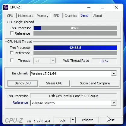

Of course, I can’t guarantee every CPU in all systems will be able to achieve this kind of overclock. This is just based on what I was able to achieve with this one CPU.
Alder Lake Overclocking: Conclusion
Alright, that’s it for this article.
As you can see there’s a lot to talk about when it comes to Alder Lake overclocking. In the coming weeks, I’ll be putting out some SkatterBencher overclocking guides for Alder Lake CPUs. So, stay tuned for that.
As per usual, if you have any questions or comments, feel free to drop them in the comment section below.
See you next time!
SkatterBencher #57: Intel UHD Graphics 770 (13th Gen) Overclocked to 2500 MHz - SkatterBencher
[…] of this overclocking guide. If you’re interested in more details about XMP 3.0, check out my Alder Lake launch […]
SkatterBencher #53: Intel Core i9-13900KS Overclocked to 6300MHz - SkatterBencher
[…] There’s a lot more to the new XMP 3.0 standard, which is outside the scope of this overclocking guide. If you’re interested in more details about XMP 3.0, check out my Alder Lake launch blog. […]
SkatterBencher #52: Intel Core i9-13900K P-core Overclocked to 6500MHz - SkatterBencher
[…] There’s a lot more to the new XMP 3.0 standard, which is outside the scope of this overclocking guide. If you’re interested in more details about XMP 3.0, check out my Alder Lake launch article. […]
Gurp
great guide, thank you
SkatterBencher #50: Intel Core i7-13700K Overclocked to 6000MHz - SkatterBencher
[…] There’s a lot more to the new XMP 3.0 standard, which is outside the scope of this overclocking guide. If you’re interested in more details about XMP 3.0, feel free to check out my Alder Lake launch article. […]
SkatterBencher #37: Intel Core i5-12400 Overclocked to 5300 MHz - SkatterBencher
[…] I had already hinted at in my launch article, non-K overclocking on Alder Lake is back. However, the enthusiastic media and hyped-up […]
SkatterBencher #34: Intel Core i9-12900KF Overclocked to 5700 MHz - SkatterBencher
[…] ElmorLabs is a company founded by former ASUS ROG motherboard engineer and extreme overclocker Elmor. He designs and sells electronic tools that help performance enthusiasts in their search of higher frequencies and better performance. For this system, I use three of his tools: […]
SkatterBencher #33: Intel UHD Graphics 770 Overclocked to 2378 MHz - SkatterBencher
[…] my Alder Lake launch article, I said that like on Rocket Lake Alder Lake does not support independent Slice and Unslice […]
Reed
WOW….what a epic guide. Thanks for that!!!
SkatterBencher #32: Intel Core i5-12600KF Overclocked to 5500 MHz - SkatterBencher
[…] I discussed this behavior in a separate article on this blog. […]