SkatterBencher #87: Core Ultra 7 265K Overclocked to 5700 MHz
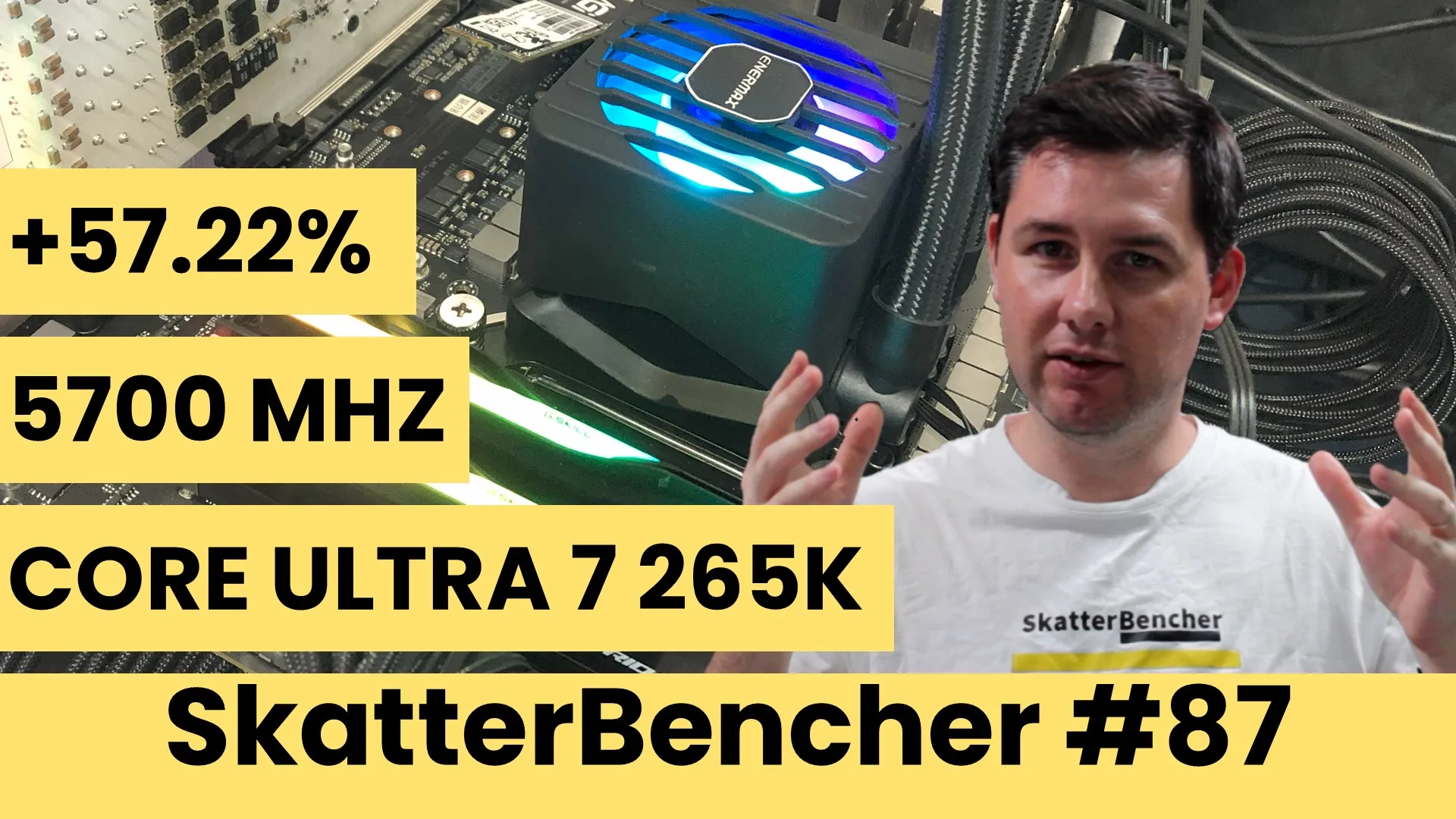
We overclock and undervolt the Intel Core Ultra 7 265K to 5700 MHz with the ASUS ROG Z890-E Gaming motherboard and AIO cooling.
We do this by exploring several of the Arrow Lake overclocking tools which I previously covered on this blog. In this post, I break down the Core Ultra 7 265K tuning process into five unique overclocking strategies for beginner and advanced overclockers.
- First, we enable Intel 200S Boost and ASUS MCE.
- Second, we do a basic tune of the CPU Cores with Turbo Ratio Limit.
- Third, we optimize the memory subsystem.
- Fourth, we finetune the CPU core overclock with OCTVB and Advanced Voltage Offset
- Lastly, we tune the DRAM timings.
This is my third Arrow Lake CPU overclocking guide and, maybe, a little less in-depth than the others. But there’s still plenty to discuss. Anyway, before we jump into overclocking, let us quickly review our system, the benchmarks, and the stock performance.
Intel Core Ultra 7 265K: Introduction
The Intel Core Ultra 7 265K is part of Intel’s Core Ultra 200S product line codenamed “Arrow Lake.” The Arrow Lake desktop processors for enthusiasts were introduced on October 24, 2024.
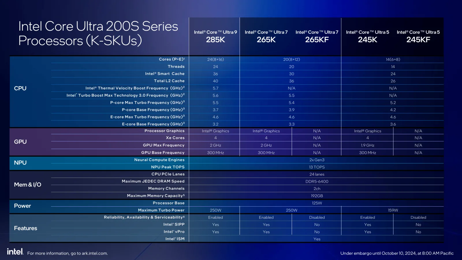
The Core Ultra 7 265K succeeds the 20-core Raptor Lake Core i7-14700K which we overclocked in SkatterBencher #68. It has a P-core base clock of 3.9 GHz and a listed Turbo Boost Max 3.0 frequency of up to 5.5 GHz. The E-cores can boost up to 4.6 GHz. The maximum rated power is 250W.
Platform Overview
The system we’re overclocking today consists of the following hardware.
| Item | SKU | Price (USD) |
| CPU | Intel Core Ultra 7 265K | 290 |
| Motherboard | ASUS ROG Strix Z890-E Gaming Wifi | 430 |
| CPU Cooling | Enermax LIQMAXFLO 420 | 120 |
| Memory | G.SKILL Trident Z5 DDR5-7800 32GB | 155 |
| Power Supply | XPG Fusion 1600W Titanium | 580 |
| Graphics Card | GALAX RTX 4090 | 1600 |
| Storage | AGI 512GB NVMe M.2 Gen3 | 75 |
| Chassis | Open Benchtable V2 | 200 |
| Telemetry | BENCHLAB | 200 |
Benchmark Software
We use Windows 11 and the following benchmark applications to measure performance and ensure system stability.
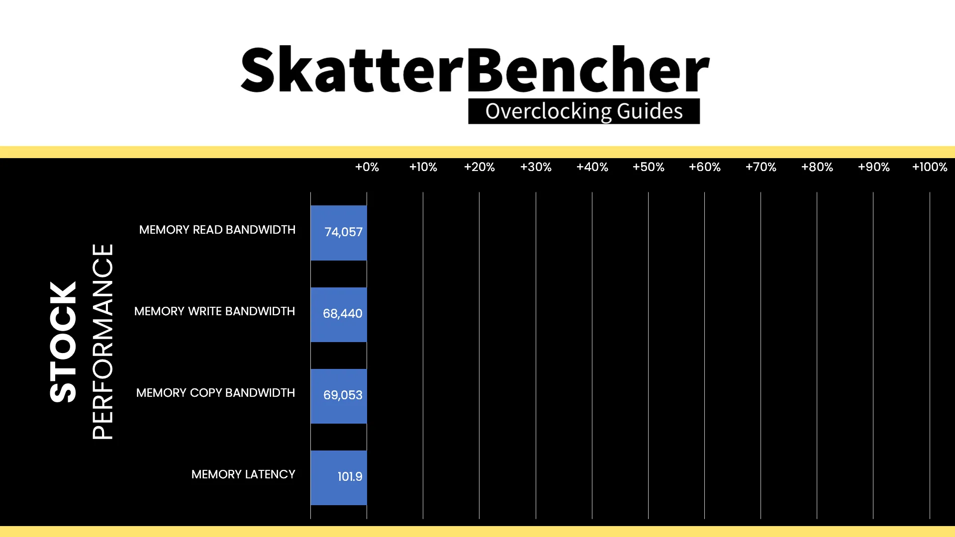
Intel Core Ultra 7 265K: Stock Performance
Before starting overclocking, we must check the system performance at default settings.
In the past, there was some confusion about what constitutes default settings for Intel processors. For Arrow Lake, Intel spent extra resources clarifying to industry and media partners what constitutes default settings.
Intel Arrow Lake Default Settings
Intel defines three power profiles for the Arrow Lake processors: baseline, performance, and extreme.
- The Baseline profile is provided for systems or motherboards with inadequate power delivery requirements to meet the performance profile. You can typically find it referenced as “Intel Default Baseline Profile.”
- The Performance profile is recommended by Intel as the default profile for most systems. In particular, high-end motherboards or gaming systems. You can typically find it referenced as “Intel Default Performance Profile.”
- The Extreme profile is provided as guidance to system designers or motherboards that intend to support overclocking. This profile is not validated by Intel and, when used, may void warranty terms.
The default settings must be in place on the first boot, after a BIOS update, or when a new CPU is installed. When users change the default settings, there should be a BIOS warning informing the users that the settings deviate from the Intel default settings.
For the purpose of this guide, we follow Intel’s direction and rely on the Performance profile for the default settings.
Intel Core Ultra 7 265K Performance Profile
The Intel Default Performance Profile configuration parameters for Arrow Lake CPUs are as follows:
| Parameter | Configuration |
| CEP (Current Excursion Protection) | Enable |
| TVB (Thermal Velocity Boost) | Enable |
| TVB Voltage Optimizations | Enable |
| DLVR Bypass | Disable |
| ICCMax Unlimited | Disable |
| TjMax Offset | 0 |
| Turbo Ratio Limit Override | No changes |
| C-states | Enable |
| Enhanced C-states (C1E) | Enable |
| AC Load Line | AC Load Line is within verified design specs |
| DC Load Line | DC Load Line = AC Load Line |
The Intel Default Performance Profile Turbo Boost 2.0 parameters for the Core Ultra 7 265K are as follows:
| Parameter | Baseline | Performance | Extreme |
| ICCMax | 287 A | 347 A | N/A |
| ICCMax_App | 210 A | 245 A | N/A |
| Power Limit 1 (PL1) | 125 W | 250 W | N/A |
| Power Limit 2 (PL2) | 177 W | 250 W | N/A |
| Power Limit 4 (PL4) | 329 W | 425 W | N/A |
The Turbo Ratio Limit parameters for the Core Ultra 7 265K are as follows:
| Parameter | Ratio |
| Up to 2 active P-cores | 55X |
| Up to 8 active P-cores | 52X |
| Up to 16 active E-cores | 46X |
| Ring | 37X |
| NGU | 26X |
| D2D | 21X |
Here is the benchmark performance at stock:
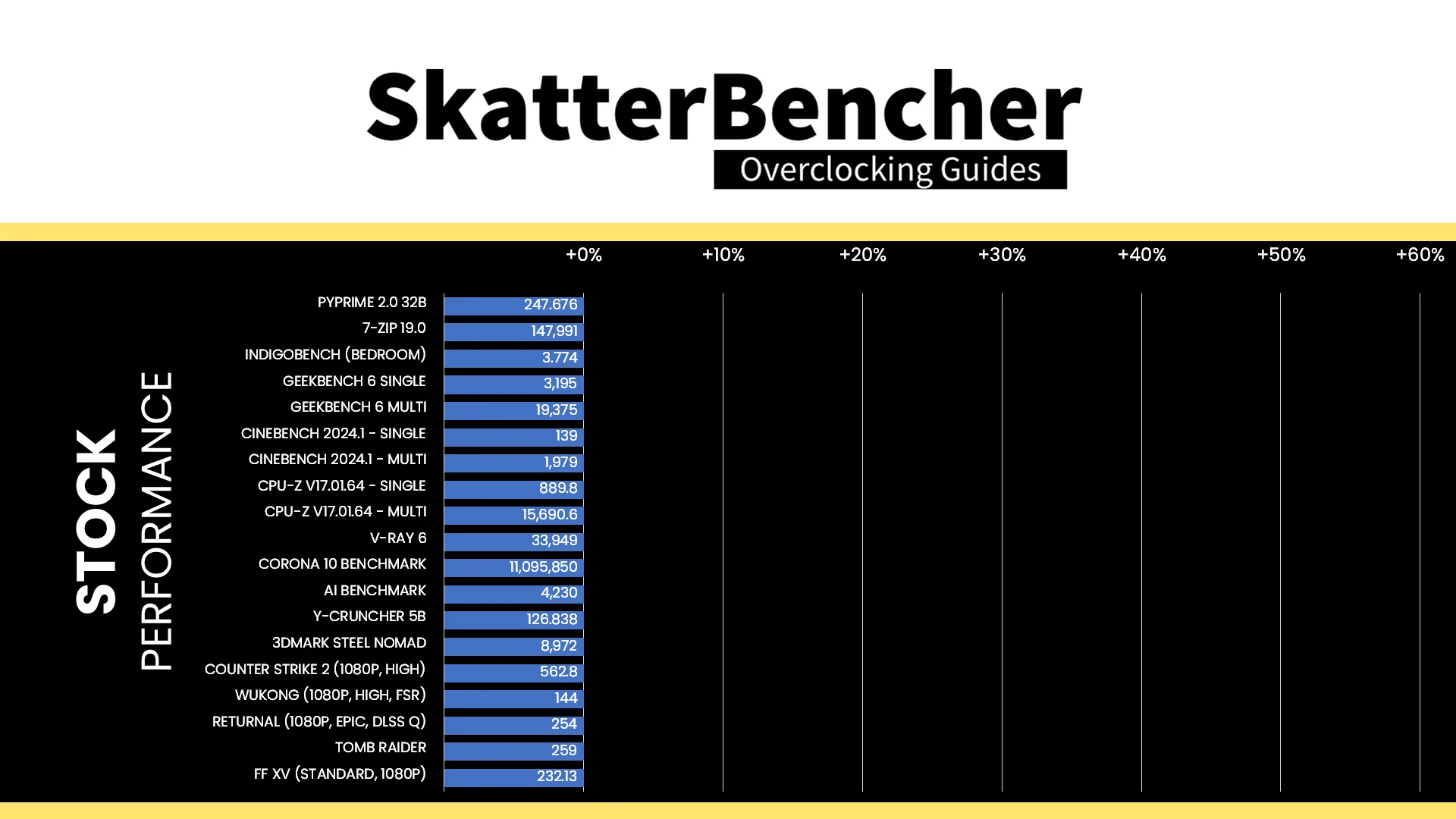
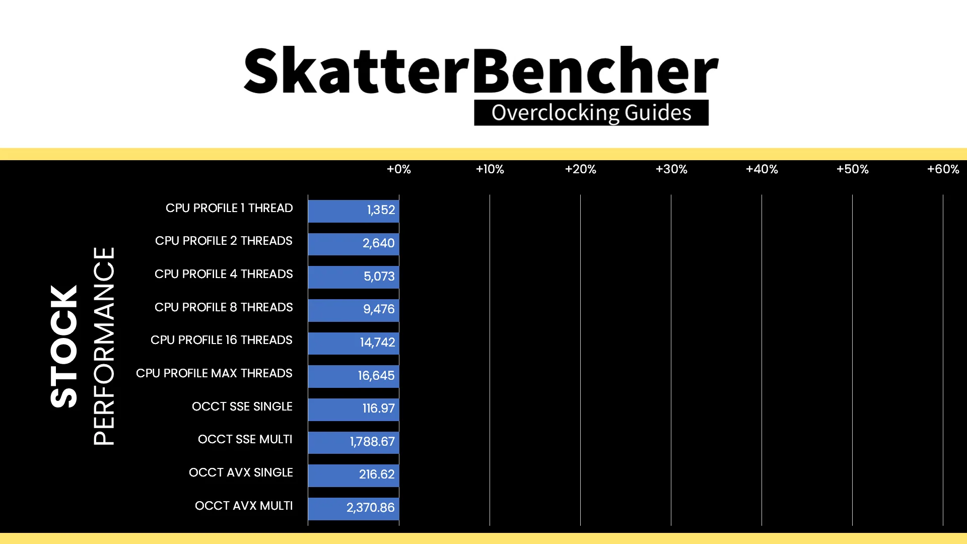
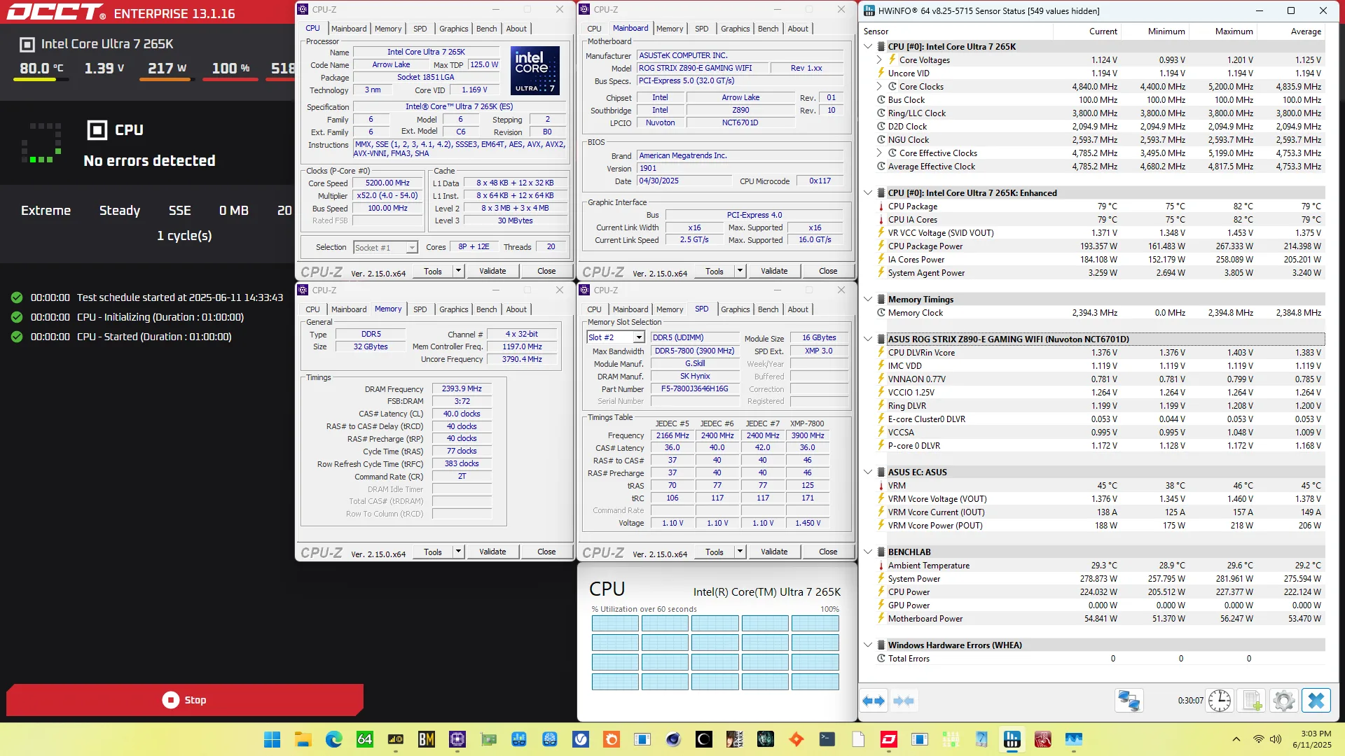
When running the OCCT CPU AVX2 Stability Test, the average CPU P-core effective clock is 5189 MHz with 1.182 volts, and the average CPU E-core effective clock is 4434 MHz with 1.090 volts. The average CPU temperature is 83.0 degrees Celsius. The average CPU package power is 232.4 watts.
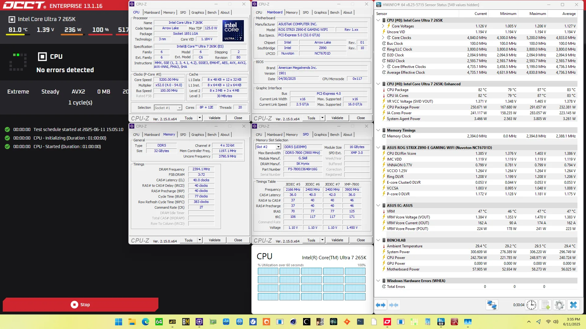
When running the OCCT CPU SSE Stability Test, the average CPU P-core effective clock is 5189 MHz with 1.177 volts, and the average CPU E-core effective clock is 4462 MHz with 1.090 volts. The average CPU temperature is 79.0 degrees Celsius. The average CPU package power is 214.4 watts.
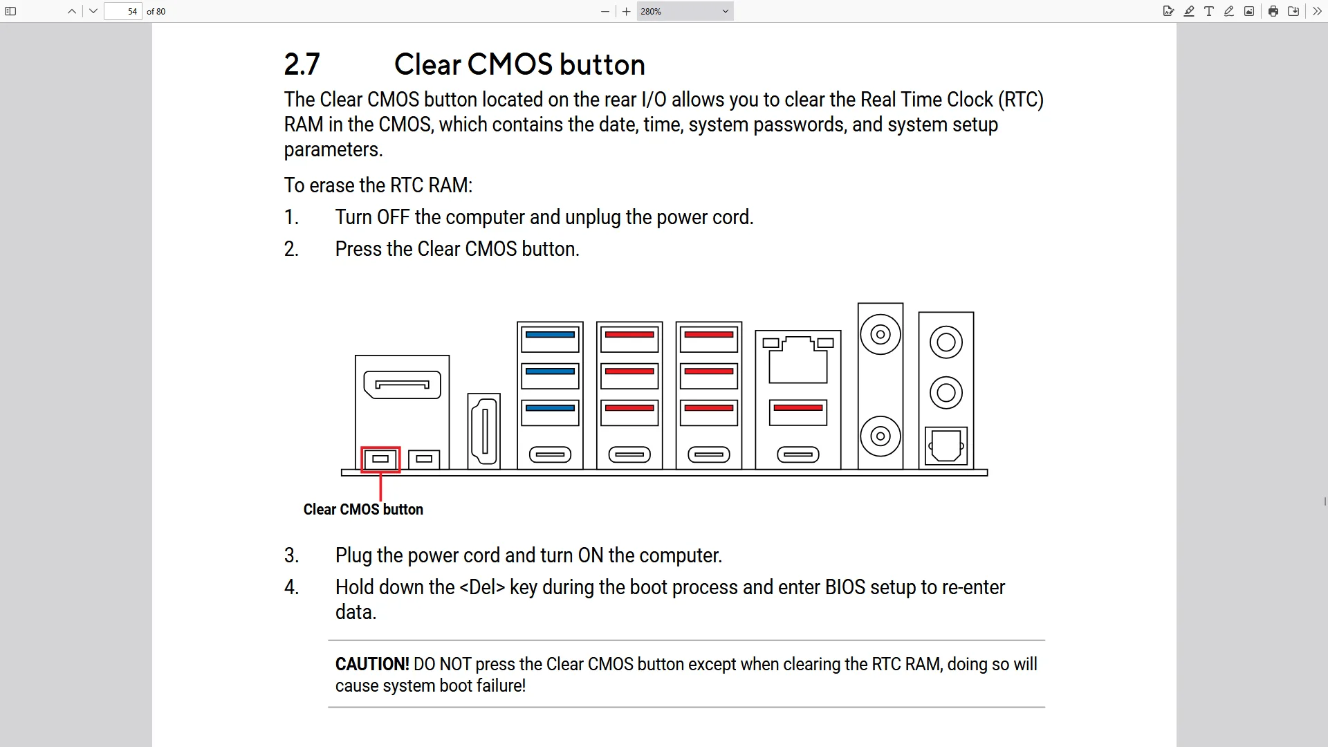
Of course, we can increase the performance by unlocking power limits and overclocking the processor. However, before we get going, make sure to locate the CMOS Clear button. Pressing the Clear CMOS button will reset all your BIOS settings to default, which is helpful if you want to start your BIOS configuration from scratch.
OC Strategy #1: 200S Boost + MCE
In our first overclocking strategy, we simply take advantage of enabling Intel 200S Boost and optimizing Intel Turbo Boost 2.0 power limits.
Intel 200S Boost
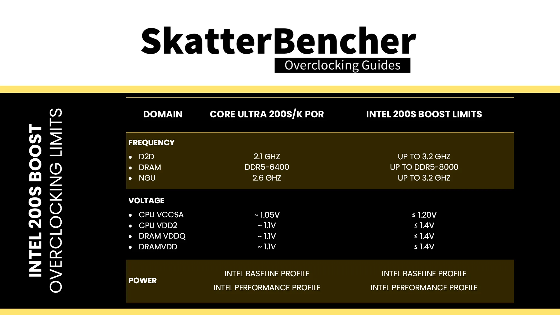
Intel 200S Boost is an Intel overclocking technology that enables NGU, D2D, and memory overclocking on Arrow Lake K-SKU processors without voiding warranty.
The 200S Boost program specifically enables for the creation of a motherboard BIOS option or profile that loads an OEM/ODM-tested set of “up to” values geared towards increasing performance on their platform. The “up to” values include restrictions on the voltage and frequency for the DRAM, D2D, and NGU.
Practically, 200S Boost is an easy way to enable XMP 3.0 without voiding the warranty because, yes, enabling XMP still technically voids warranty. In addition to enabling XMP, 200S Boost also sets the NGU and D2D ratio to 32X as well as increase the VccSA voltage to 1.2V.
Intel Turbo Boost 2.0 Power Limits
Intel Turbo Boost 2.0 Technology allows the processor cores to run faster than the base operating frequency if the processor is operating below rated power, temperature, and current specification limits. The ultimate advantage is opportunistic performance improvements in both multi-threaded and single-threaded workloads.
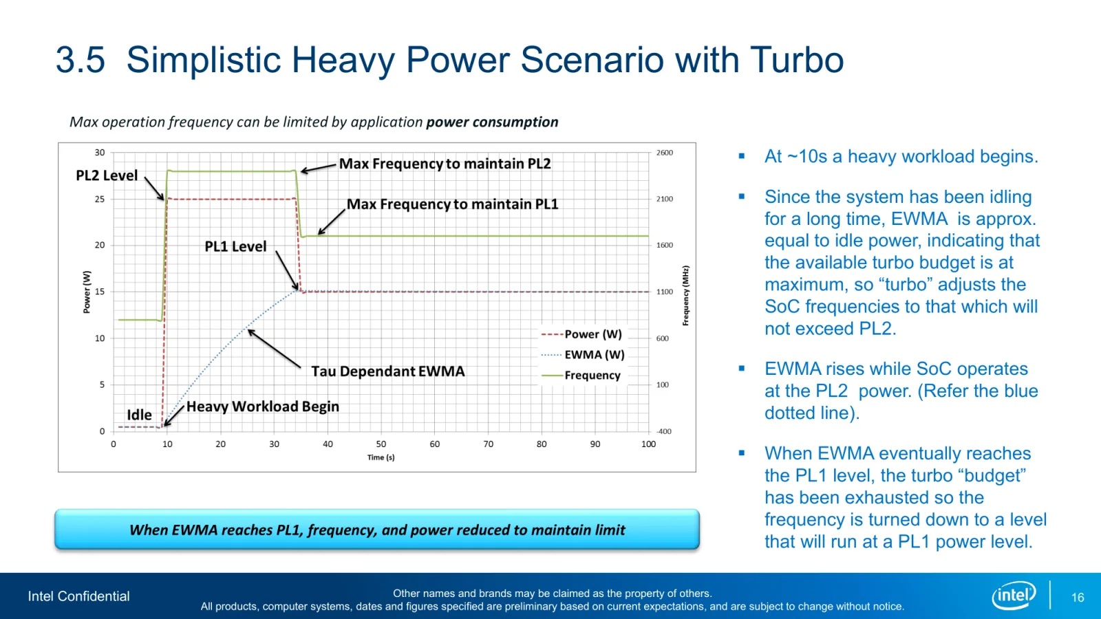
The turbo boost algorithm works according to an EWMA formula. This stands for Exponentially Weighted Moving Average. There are three main parameters to consider: PL1, PL2, and Tau.
- Power Limit 1, or PL1, is the threshold that the average power will not exceed. Historically, this has always been set equal to Intel’s advertised TDP. Very importantly, PL1 should not be set higher than the thermal solution cooling limits.
- Power Limit 2, or PL2, is the maximum power the processor is allowed to use for a limited amount of time.
- Tau is a weighing constant used in the algorithm to calculate the moving average power consumption. Tau, in seconds, is the time window for calculating the average power consumption. If the average power consumed is higher than PL1 the CPU will reduce the CPU frequency.
Turbo Boost 2.0 Technology has evolved over the past years to incorporate a lot of power, thermal, and electrical performance limiters, including PL3, PL4, IccMax, TCC_Offset, VR_TDC, RATL, Pmax, and many more.
An easy ASUS MultiCore Enhancement option on ASUS motherboards allows you to unleash the Turbo Boost power limits. Set the option to Enabled – Remove All Limits and enjoy maximum performance.
BIOS Settings & Benchmark Results
Upon entering the BIOS
- Go to the Ai Tweaker menu
- Set Performance Preferences to Intel Default
- Set Intel Default Settings to Performance
- Set Intel 200S Boost to Enabled
- Set ASUS MultiCore Enhancement to Enabled – Remove All Limits
Then save and exit the BIOS.
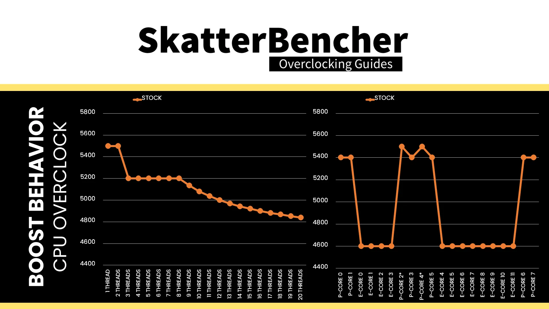
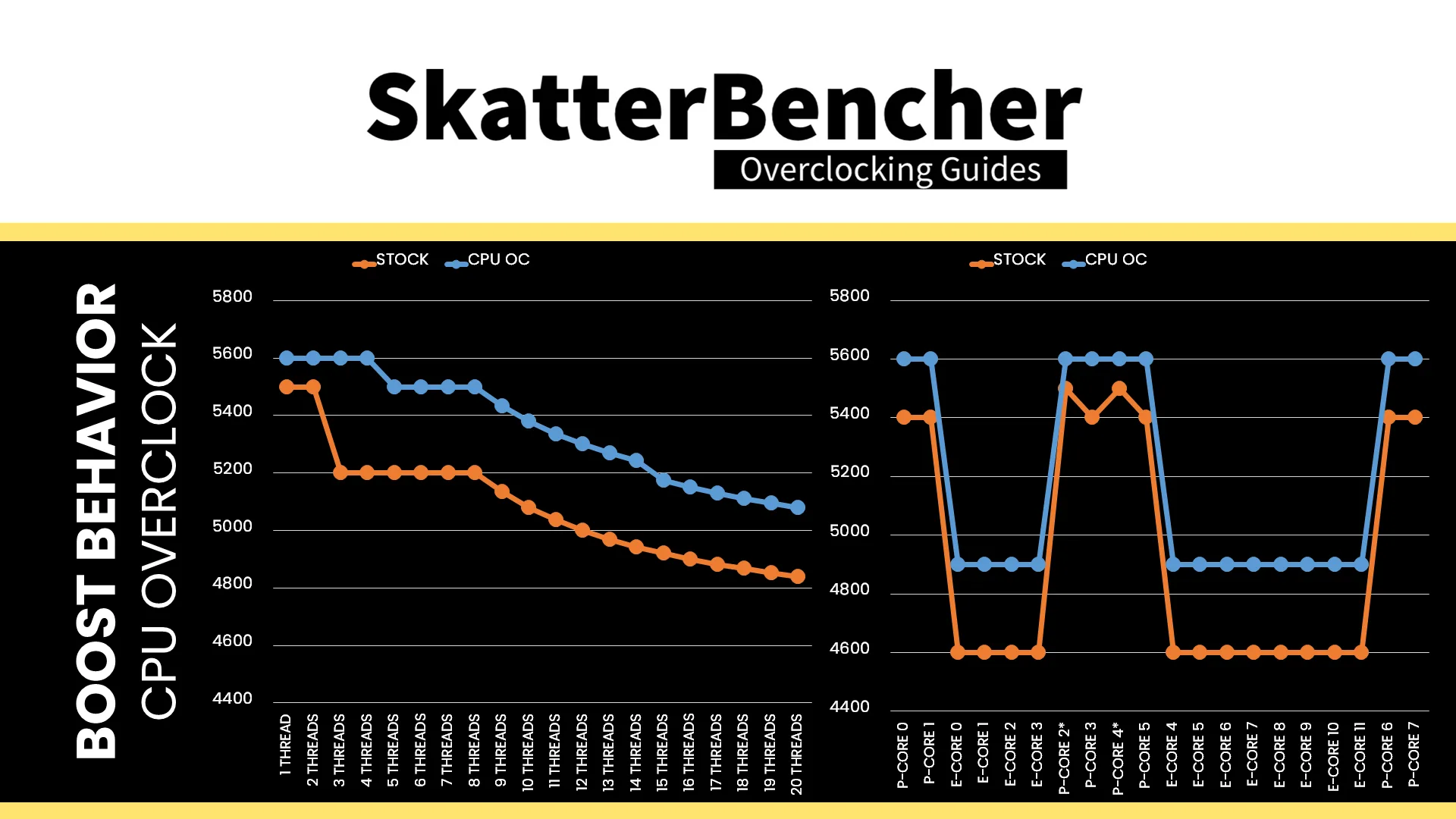
The CPU boost frequency with 1 active P-core is 5500 MHZ. The average boost frequency gradually trails off to 5200 MHz when all P-cores are active and to 4840 MHz when all P- and E-cores are active. The two favored P-cores can boost to 5.5 GHz, the six other non-favored cores can boost to 5.4 GHz, and every E-core can boost to 4.6 GHz in single-threaded workloads.
We re-ran the benchmarks and checked the performance increase compared to the default operation.
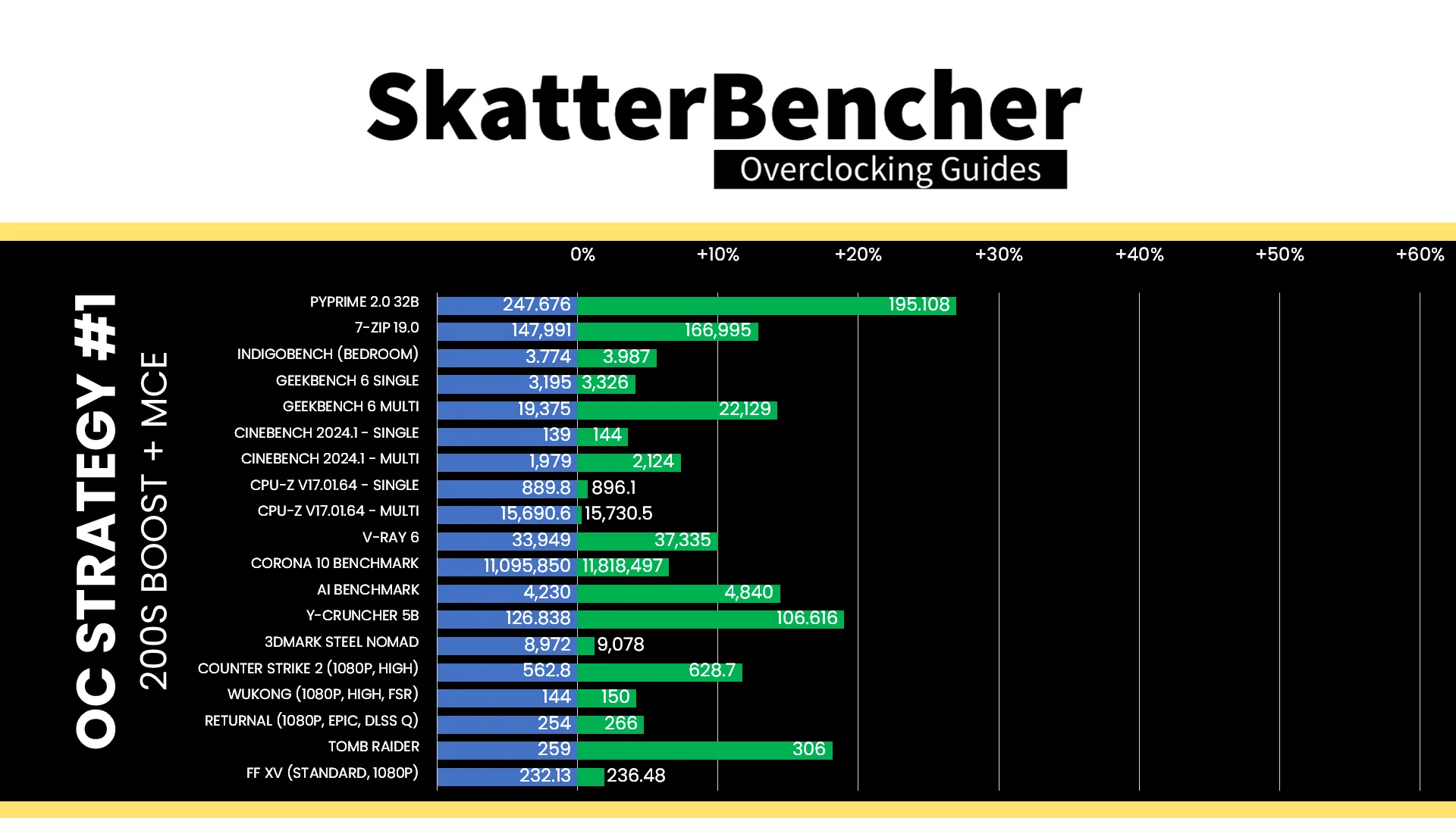
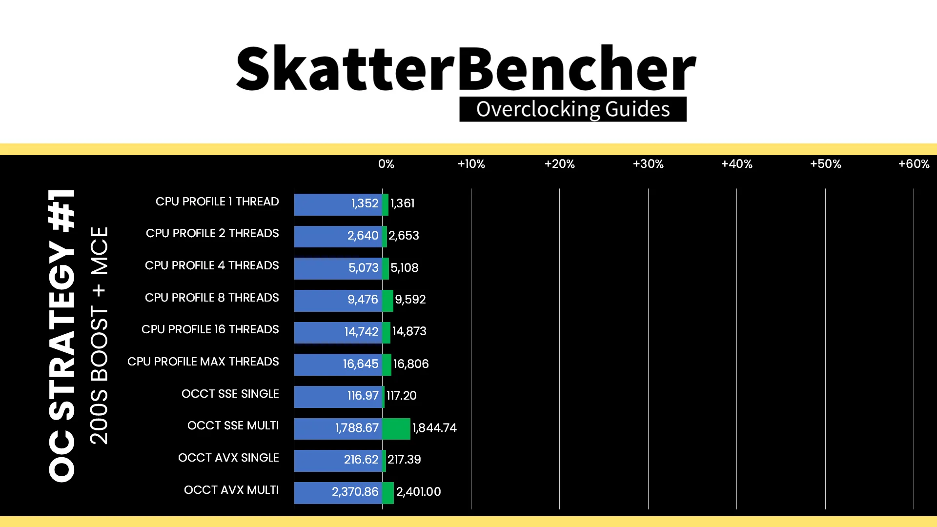
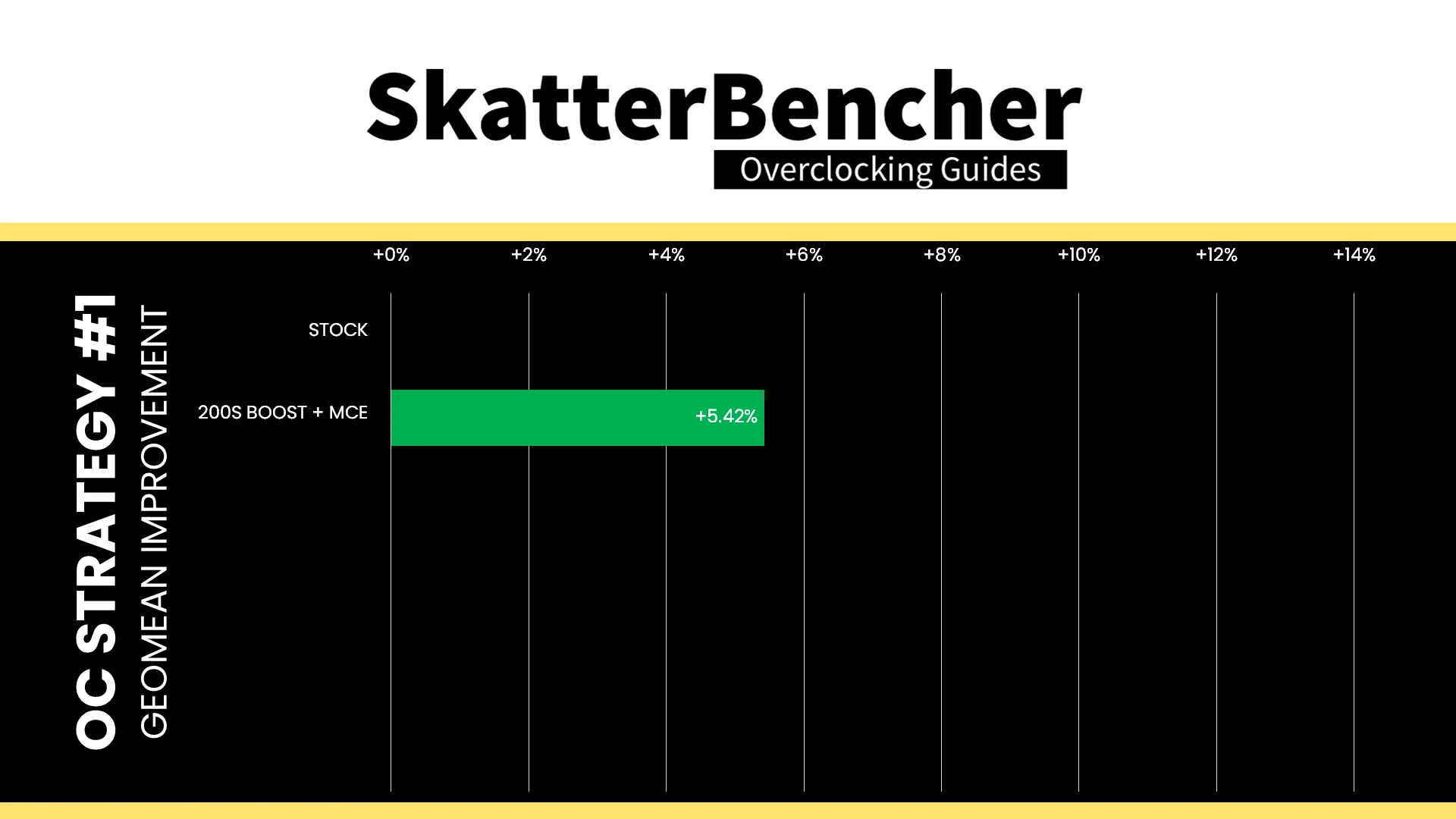
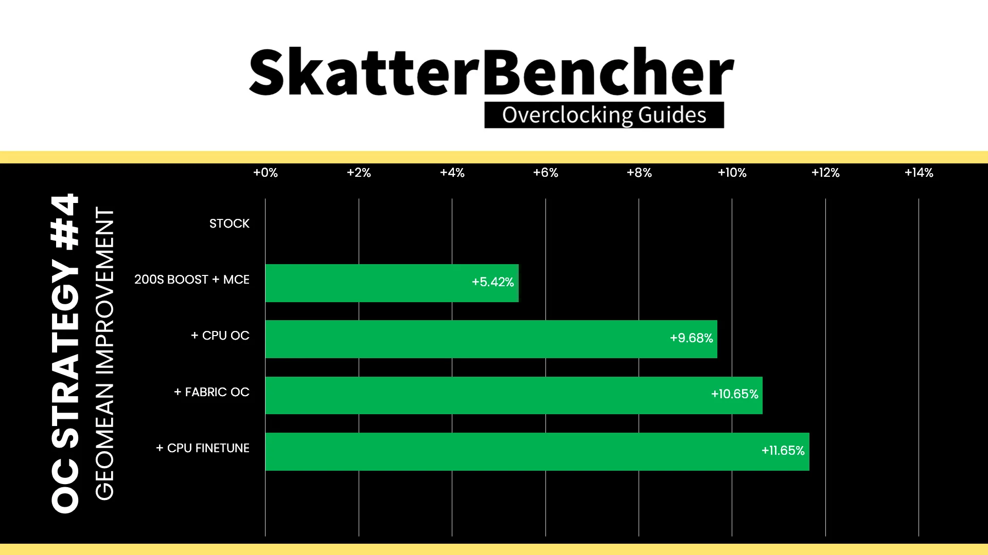
Intel 200S Boost isn’t a very complicated technology as it just enables XMP and optimizes the fabric speed. However, in tandem with unleashing the power limits, it translates in a pretty neat performance uplift. Especially in multi-threaded, memory-hungry applications like Y-Cruncher and AI Benchmark. The Geomean performance improvement is +5.43%, and we get a maximum improvement of +26.94% in PyPrime.
When running the OCCT CPU AVX2 Stability Test, the average CPU P-core effective clock is 5193 MHz with 1.183 volts, and the average CPU E-core effective clock is 4601 MHz with 1.092 volts. The average CPU temperature is 87.0 degrees Celsius. The average CPU package power is 254.0 watts.

When running the OCCT CPU SSE Stability Test, the average CPU P-core effective clock is 5194 MHz with 1.177 volts, and the average CPU E-core effective clock is 4594 MHz with 1.090 volts. The average CPU temperature is 80.0 degrees Celsius. The average CPU package power is 227.5 watts.

OC Strategy #2: CPU Overclock
In our second overclocking strategy, we finally overclock the CPU cores. For this we rely on two foundational overclocking technologies: Turbo Ratio Limit and Adaptive Voltage mode.
Turbo Ratio Limit
Intel Turbo Ratio Limit is a technology that regulates the Turbo Boost frequency of an Intel processor based on the number of active cores.
Intel processors usually have two types of CPU core frequencies specified: the base frequency and the Turbo Boost frequency. The base frequency is also known as the “Maximum Non-Turbo Ratio” whereas the turbo frequency is usually referred to as the Turbo Ratio Limit.
The Turbo Ratio Limit is called a limit because it restricts the operating frequency rather than targets a frequency. Processors like the Core Ultra 7 265K have an upper core frequency ratio of 120X. Without the ratio limit, the CPU would boost its frequency all the way to the maximum frequency. However, the Turbo Ratio Limit specifies an upper ceiling to the boost frequency.
The tool is pretty flexible and can be programmed for various scenarios. The ratio limits are defined in the processor’s Machine Specific Registers (MSRs) by two parameters:
- The Turbo Ratio Limit
- The number of active cores
For CPUs like the Core Ultra 7 265K, which have no more than 8 P-cores, these registers are configured from 1-active P-core to 8-active P-cores. However, on platforms with core counts beyond eight cores, we can configure each register by target Turbo Boost Ratio and the number of active cores.
Furthermore, on hybrid designs like Alder Lake, Raptor Lake, or Arrow Lake, which all feature a combination of P-cores and E-cores, the Turbo Ratio Limit configuration is specified by core type. In other words: the applied ratio limit for the P-cores is independent from the limit of the E-cores.
For example, on the Core Ultra 7 265K the Turbo Ratio Limit specifies 55X when up to 2 P-cores are active, 52X when 3 or more P-cores are active, and 46X for any amount of active E-cores. In theory, if 2 P-cores and all E-cores are active, the P-cores would operate at 55X even though more than 2 cores in total are active.
Note that configuring the turbo ratio is not the same as configuring each core individually. When using turbo ratio limit, we determine an overclock according to CPU usage. For example, if a workload uses four cores, the CPU determines which cores should execute this workload and applies our set frequency to those cores.
The Turbo Ratio Limit configuration also has a couple of rules that must be followed:
- Each register must be defined by a target ratio and a number of active cores.
- The minimum allowed ratio limit is the maximum non-turbo ratio.
- The maximum allowed ratio limit is defined per architecture.
- On modern CPUs that’s 85X or 120X using extended ratio mode
- The ratio limit of a register must be equal to or lower than the ratio defined for the previous register .
- E.g. we cannot define 60X for up to 1 active core and 62X for up to 4 active cores.
- The core count of a register must be equal to or lower than the ratio defined for the previous register.
- E.g. we cannot define register 1 to define the ratio for up to 5 active cores and register 2 to define the ratio for up to 2 active cores
- The last register must always define the ratio limit for the highest available active cores of the processor SKU.
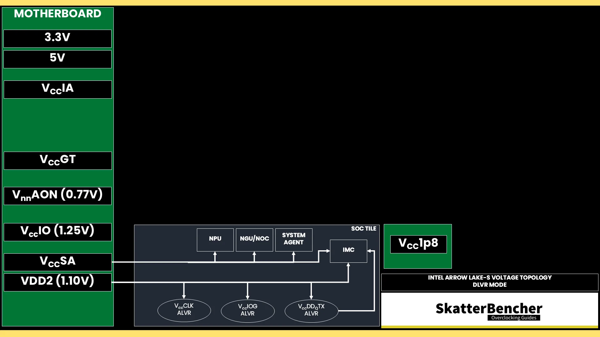
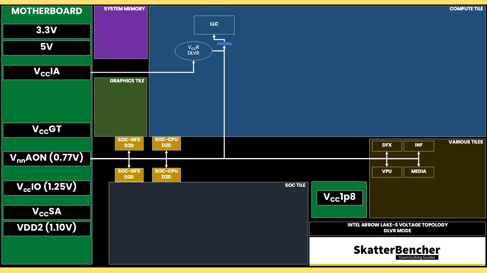
Arrow Lake Voltage Topology
The voltage regulation for the P-cores is more complex than prior generations of Intel Core processors due to the introduction of the Digital Linear Voltage Regulator (DLVR). The DLVRs enable much lower voltage levels for the cores and ring but still rely on a dynamic external motherboard voltage regulator as the input voltage source.
VccIA, VccCORE, & VccATOM
The external VccIA motherboard voltage regulator (MBVR) provides the input voltage for the individual P-core, E-core clusters, Ring, last-level cache (LLC), and E-core L2 cache. Each P-core, E-core cluster, and Ring has an individual Digital Linear Voltage Regulator (DLVR) between the VccIA rail and the IP blocks. That means each of the blocks can operate at its own voltage.
- VccCOREn is the DLVR powering an individual P-core.
- VccR is the DLVR powering the Ring and Last-Level Cache.
- VccATOMn is the DLVR powering an individual E-core cluster, which consists of four E-cores, and its L2 cache.
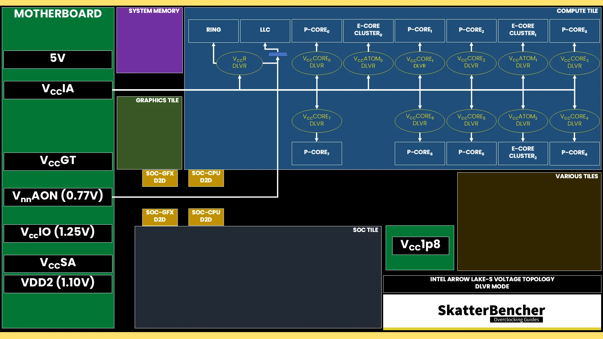
The DLVRs can also be bypassed. In that case, the IP blocks are running in so-called Power Gate (PG) mode. I covered that in depth when overclocking the Core Ultra 5 245K and the Core Ultra 9 285K.
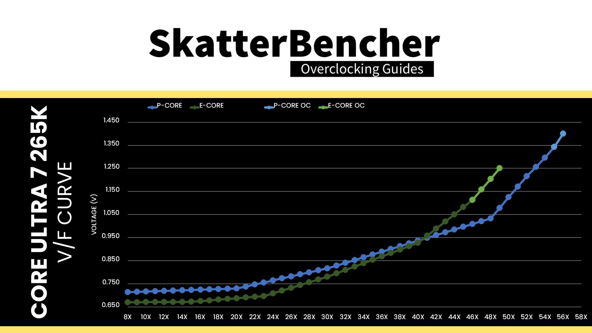
V/F Curves
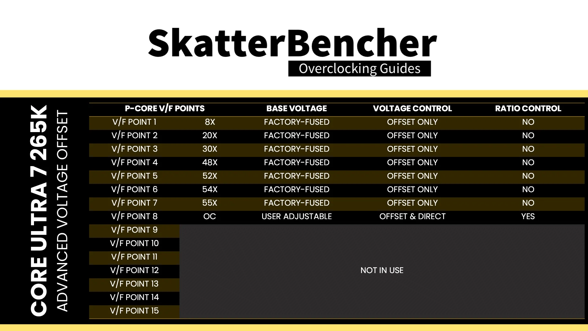
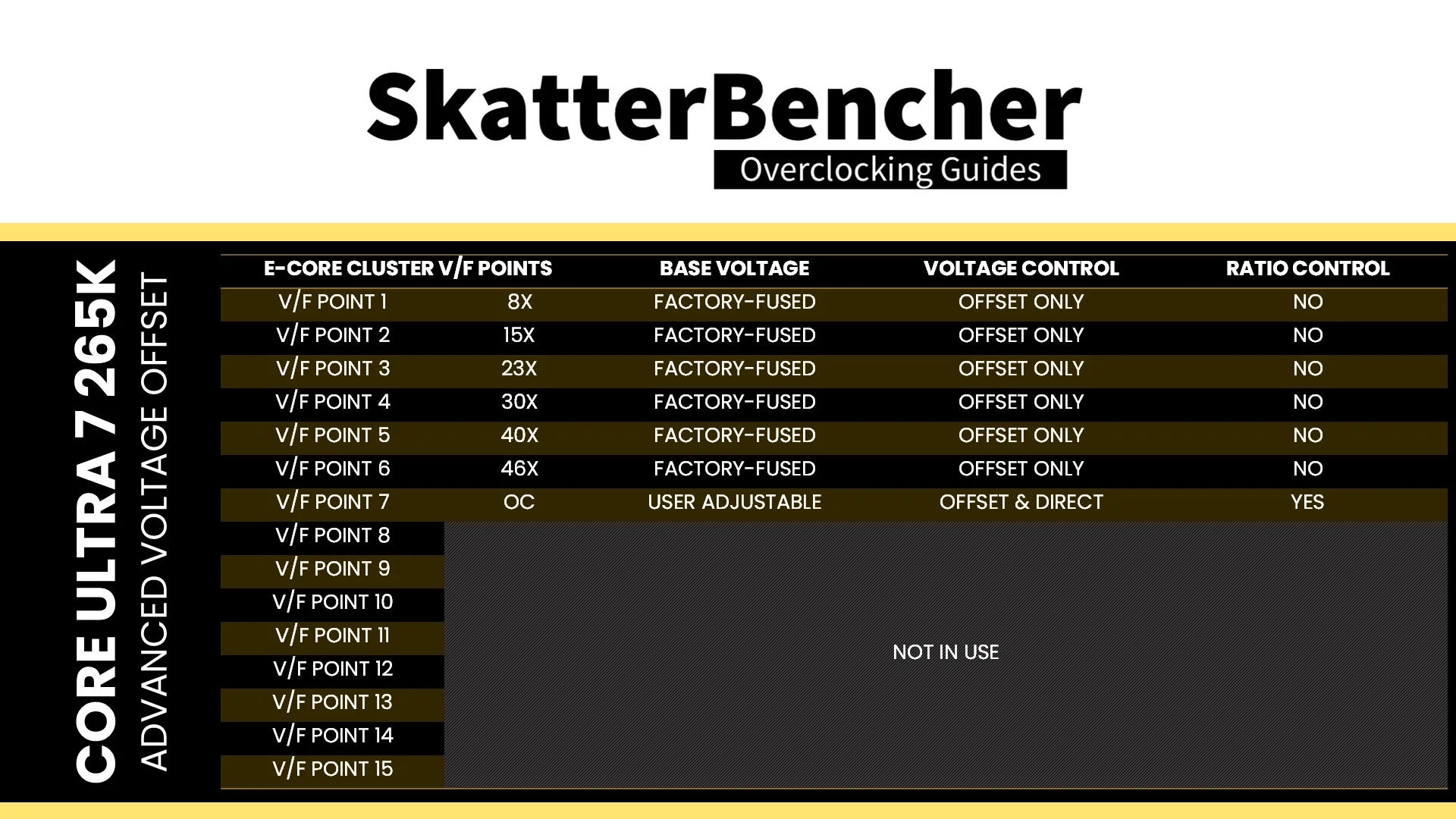
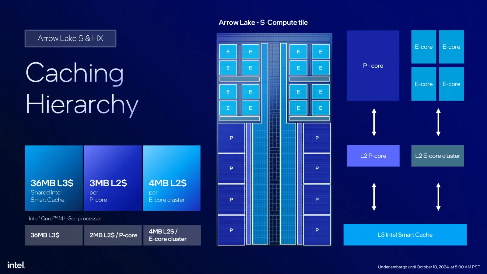
Each Core Ultra 7 265K P-core and E-core cluster also has its own V/F curve which is defined by eight (8) V/F points for the P-cores and seven (7) V/F points for the E-core clusters. For the P-cores, the first seven (7) V/F points are factory-fused, and the last point is mapped to the “OC Ratio.” For the E-cores, the first six (6) V/F points are factory-fused, and the last point is mapped to the “OC Ratio.”
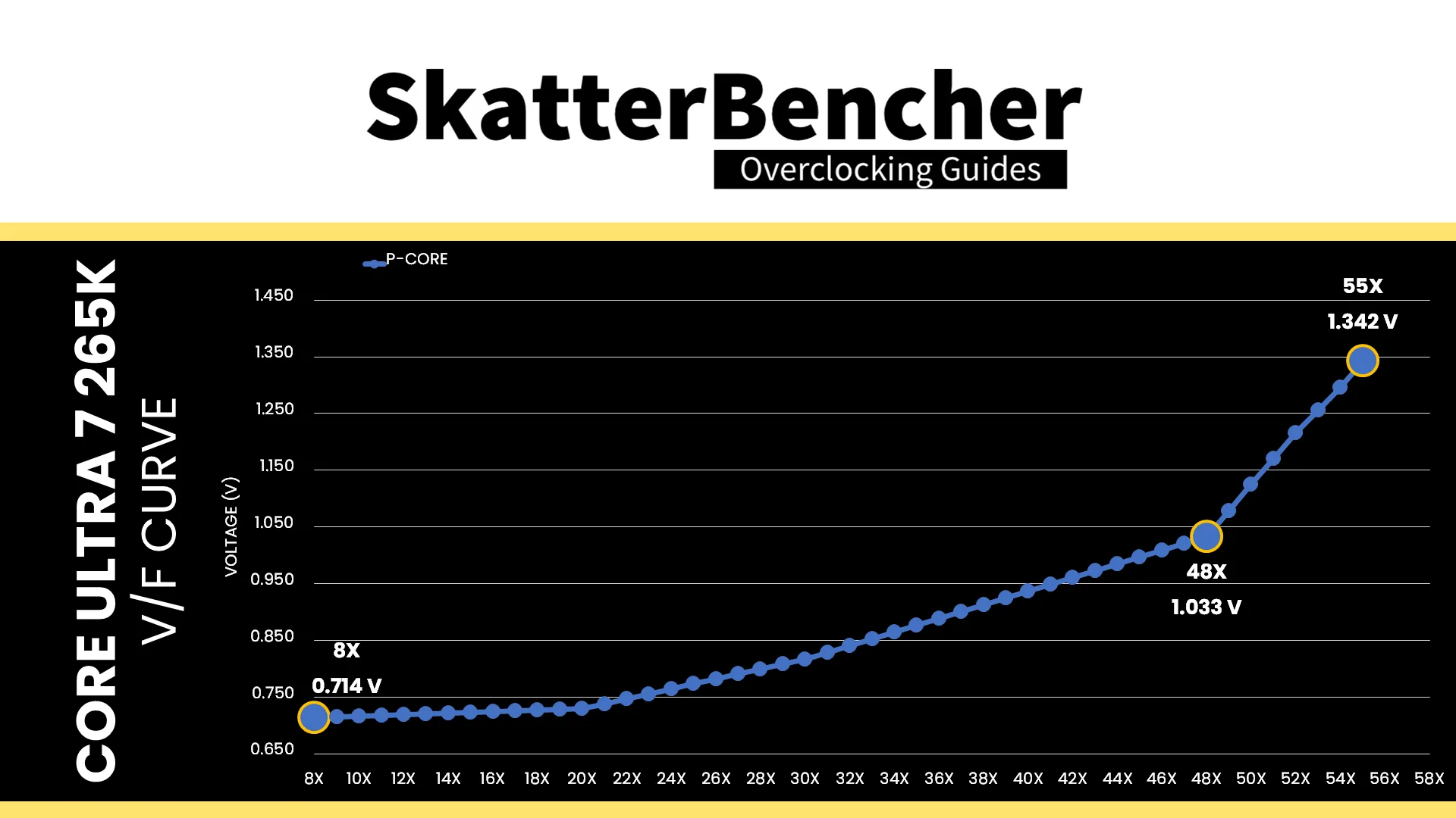
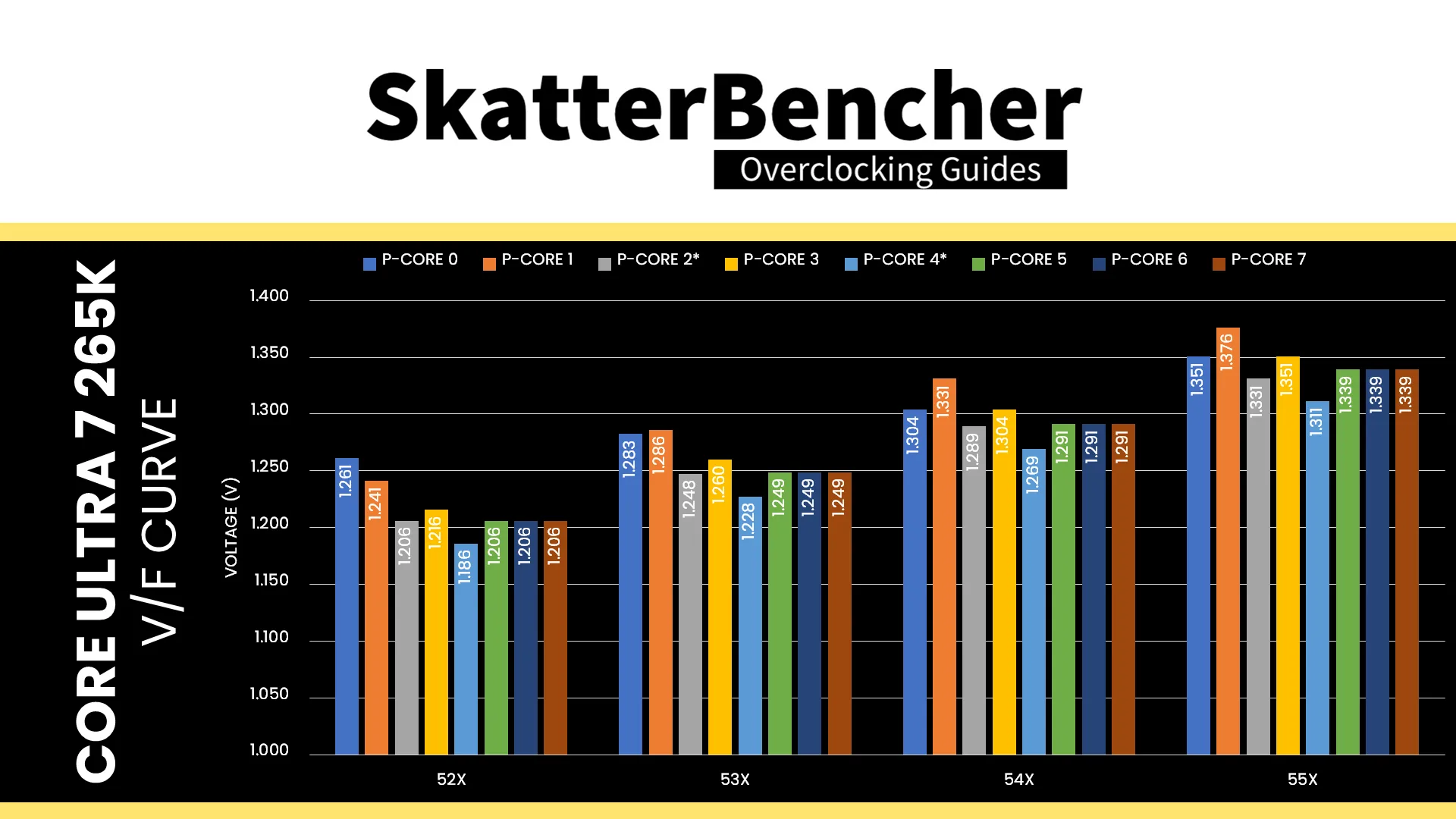
Here is the aggregate P-core V/F curve for my specific Core Ultra 7 265K. The voltage is about 714 mV at 800 MHz, then increases to 1.033V for VF Point 4 at 4.8 GHz, and ultimately ends at 1.342 V for V/F Point 7 at 5.5 GHz. Each P-core has a different fused voltage for V/F Point 7 which ranges from 1.311V for P-core 4 to 1.376V for P-core 1.
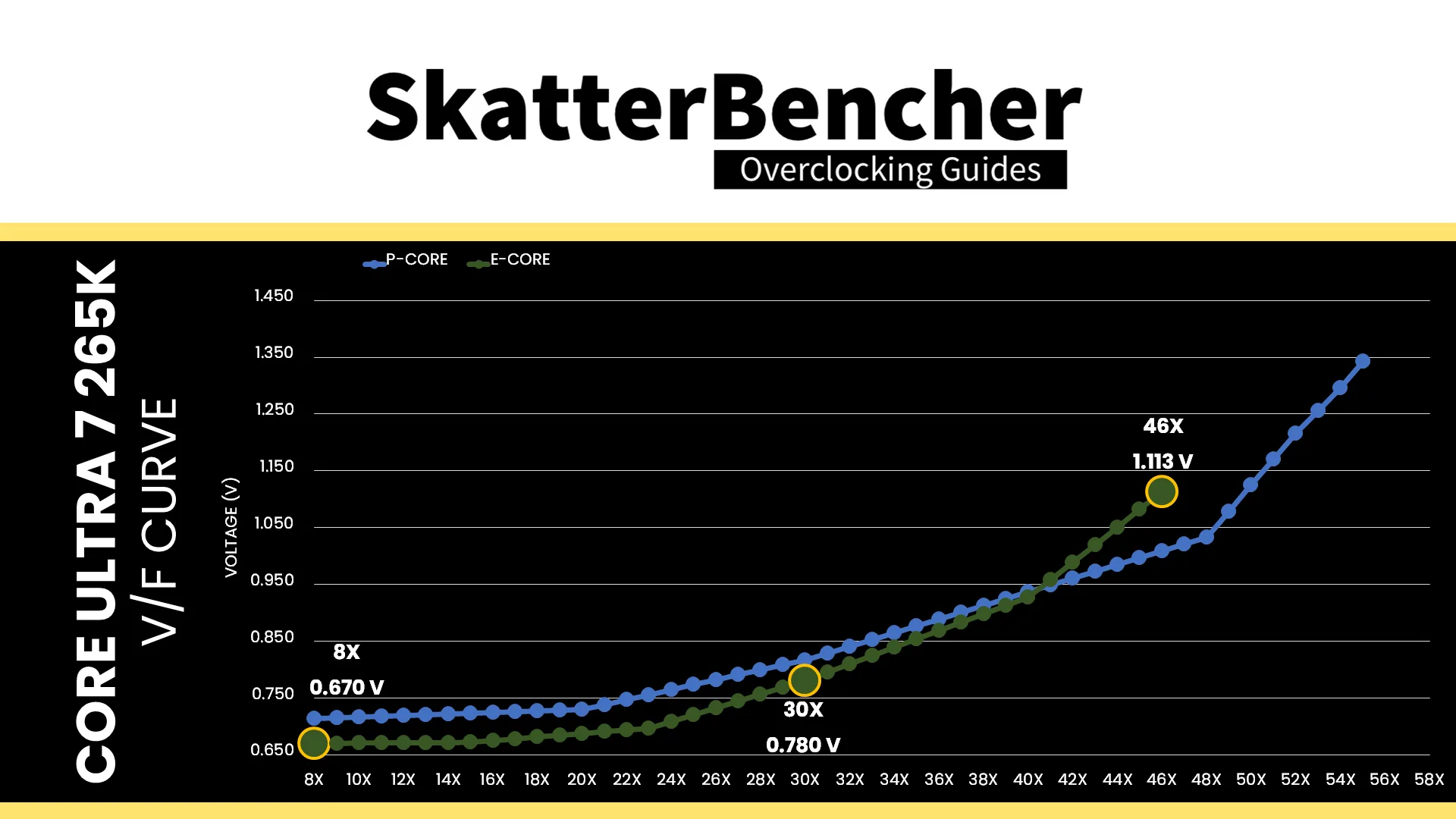
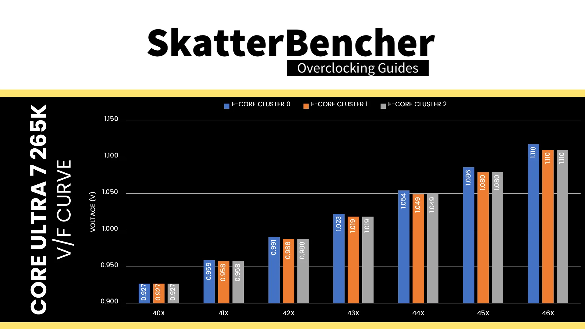
Here is the aggregate E-core V/F curve for my specific Core Ultra 7 265K. The voltage is about 670 mV at 800 MHz, then increases to 780 mV for VF Point 4 at 3.0 GHz, and ultimately ends at 1.113V for V/F Point 6 at 4.6 GHz. Each E-core has a different fused voltage for V/F Point 6 which ranges from 1.110V for E-core clusters 1 and 2 to 1.118V for E-core cluster 0.
Adaptive Voltage Mode
Based on the VF curve, the CPU cores request an operating voltage using the SVID protocol from the CPU Power Control Unit (PCU). The PCU in turn configures the VccIA voltage rail and the individual DLVRs. There are two ways to configure the DLVR voltage:
- Adaptive mode is the standard mode of operation, which relies on the factory-fused voltage-frequency curves we discussed before.
- Override mode specifies a single static voltage across all ratios. It is mainly used for extreme overclocking where stability at high frequencies is the only consideration.
We can configure override and adaptive modes directly in the PCU by specifying a target voltage and a voltage offset for each mode.
In adaptive mode, the target voltage is mapped to a core’s “OC Ratio.” Each P-core and E-core cluster has its own “OC Ratio” which is defined by the Per Core Ratio Limit. This also matches V/F Point 8 for the P-cores and V/F Point 7 for the E-cores. You can configure the adaptive voltage and OC Ratio to any value; however, multiple rules enforce what ratio and voltage are actually set.
Rule #1: the voltage set for a given VF Point n must be higher than or equal to the voltage set for VF Point n-1.
That means the voltage for the OC Ratio, matching V/F Point 8, must be higher than or equal to the voltage for VF Point 7.
For example, let’s say you set the P-core 0 Per Core Ratio Limit to 58X and the adaptive voltage to 1.1V. In that case, VF Point 8 will be programmed to 58X at 1.1V. However, the actual V/F point will be 5.8 GHz with 1.35V, as that’s that core’s voltage for VF Point 7.
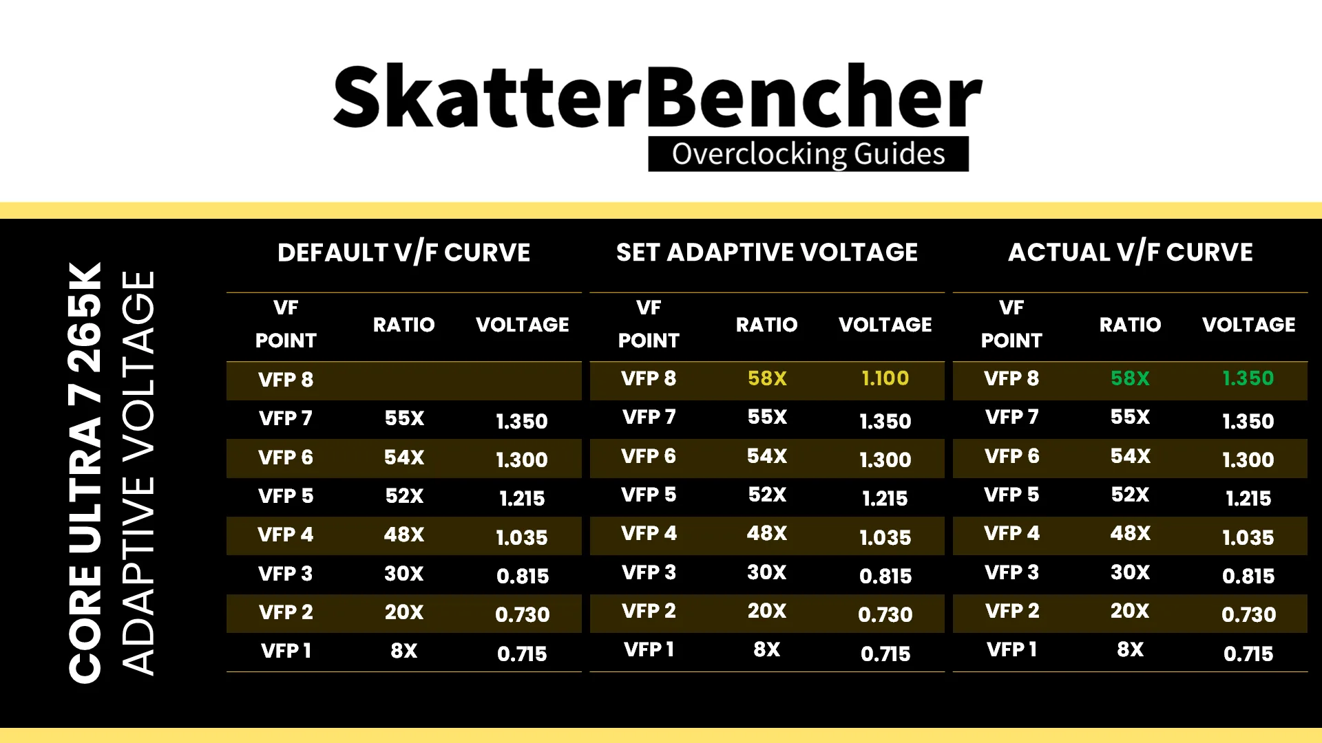
Even if you set the voltage lower in BIOS, the PCU will override your configuration if it doesn’t follow the rules.
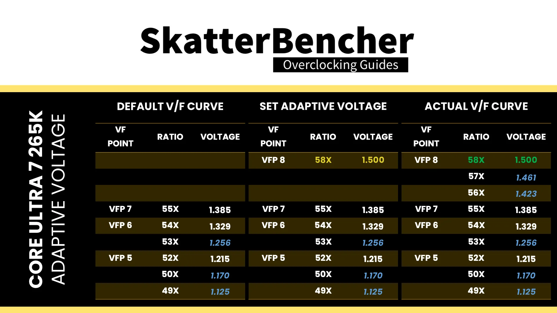
Rule #2: for ratios between the OC Ratio and the next highest factory-fused V/f point, the voltage is interpolated between the set adaptive voltage and the factory-fused voltage.
Let’s say we configure the P-core 0 V/F OC Point to 58X and 1.50V. The target voltage for each P-core ratio between 55X and 58X is now interpolated between the P-core’s factory-fused voltage for 55X and the set adaptive voltage for 58X.
There are several ways to configure the adaptive voltage, including setting it for each P-core and E-core cluster individually. In this OC Strategy, we set a single, global adaptive voltage that’s used for every core’s “OC Ratio.”
Voltage Limits
To safeguard the processor, for the first time, Intel imposes strict voltage limits for several IP blocks, including the P-cores and E-cores. This voltage limit effectively prevents the cores from requesting a higher voltage from the PCU.
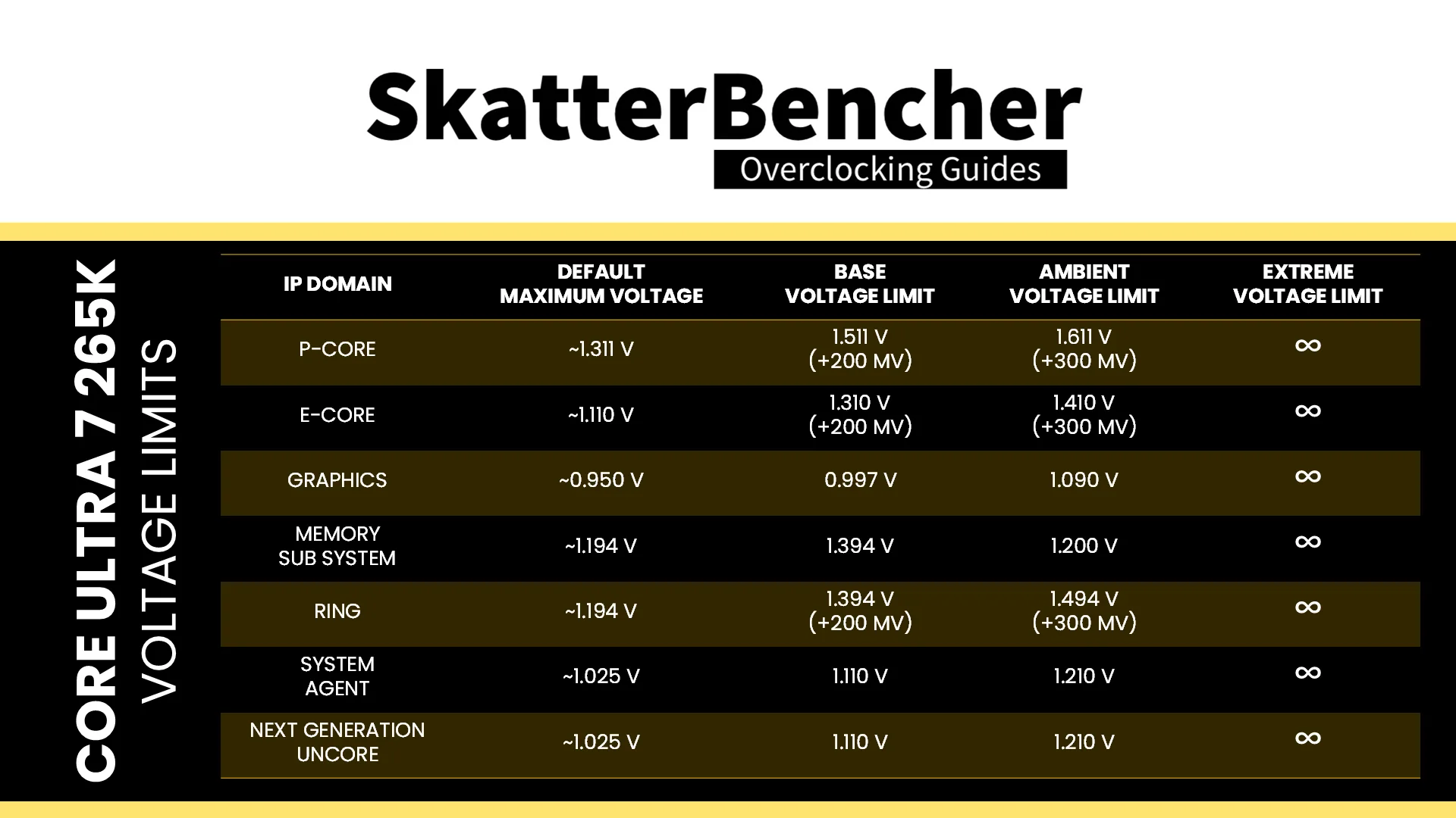
By default, the voltage limit for the P-cores and E-cores is approximately +200 mV above the lowest VID for the P-cores’ V/F Point 7 and E-core’s V/F Point 6. For this CPU’s P-cores, that’s 1.311V + 200 mV = 1.511V and for the E-cores it’s 1.110 V + 200mV = 1.310V. However, we can manually increase that to +300 mV under ambient conditions, so 1.611V and 1.410V respectively.
If you try setting the limit above the approved limit, the PCU will automatically adjust it to the highest allowed limit. If you disable voltage limits and the temperature is above 10 degrees Celsius, the CPU will operate in “safe mode” and limit the frequency to 400 MHz.
Arrow Lake P-core and E-core Tuning Process
The manual tuning process for Arrow Lake can be difficult because there’s a wide range of workload and operating scenarios to test. Furthermore, as you’ll get to see in throughout this guide, the Core Ultra 7 265K CPU cores don’t have that much overclocking headroom and don’t scale particularly well with voltage.
We can break down the basic tuning process into three steps: choosing the voltage, checking for per core stability, then lastly adjusting for all-core stability.
Choosing the Voltage
Usually, I determine an appropriate starting point for the adaptive voltage by first considering the current maximum voltage and then adding 50 to 200mV.
For example, the default maximum voltage for this CPU is 1.331V for favored P-core 2, so I decided to add +70 mV headroom and set the P-core adaptive voltage to 1.4 V. For the E-cores, the maximum voltage is 1.118V, so I added +130 mV and set it to 1.25V.
Note that we want full control over the effective voltage, so make sure to disable any technologies that might adjust the operating voltage such as TVB or Advanced Voltage Offset.
1T Stability
After you’ve set your target adaptive voltage, you can find the maximum stable frequency for each P-core and E-core cluster at that voltage. The easiest way to do that is by setting the Turbo Ratio Limit to, for example, 60X, and then setting the Per Core Ratio Limit to the frequency you want to test. For example, a starting point of 55X for the P-cores and 48X for the E-cores.
Now, you can run a stress of choice. I typically rely on the OCCT CPU Stress Test which has a built-in core cycling function. But you can also run a custom application like Core Cycler or pick a different stress test. You can start with a 30 second quick test first to quickly find the upper limit, then longer test times to confirm stability.
Strangely enough, for Arrow Lake, I found AI Benchmark to be the most difficult benchmark to pass with a high Per P-core Core Ratio Limit despite it being a multi-threaded benchmark. I attribute this to the benchmark being a highly transient, memory-dependent AVX workload. It seems that the combination of a demanding workload and dynamic power profile causes it to be the main constraint for stabilizing high frequencies.
nT Stability
Finally, we need to check if the CPU is also stable in non-single-thread workloads. The easiest way to do this is by running your worst-case all-core workload which, in my case, is always 30 minutes of OCCT CPU AVX2 Stability Test.
You’ll typically find that the CPU cannot run all-core at the same frequency as it can run single-threaded workloads. If that’s the case, simply lower the Turbo Ratio Limit for all-core workloads until it’s stable.
In addition to the OCCT CPU AVX2 Stability Test, I generally also include three other workloads during all-core testing: Y-Cruncher, Cinebench R23, and AI Benchmark. While these three test are no replacement for the worst-case stress test, they highlight different kinds of instabilities – usually related to transient loads.
Final Result
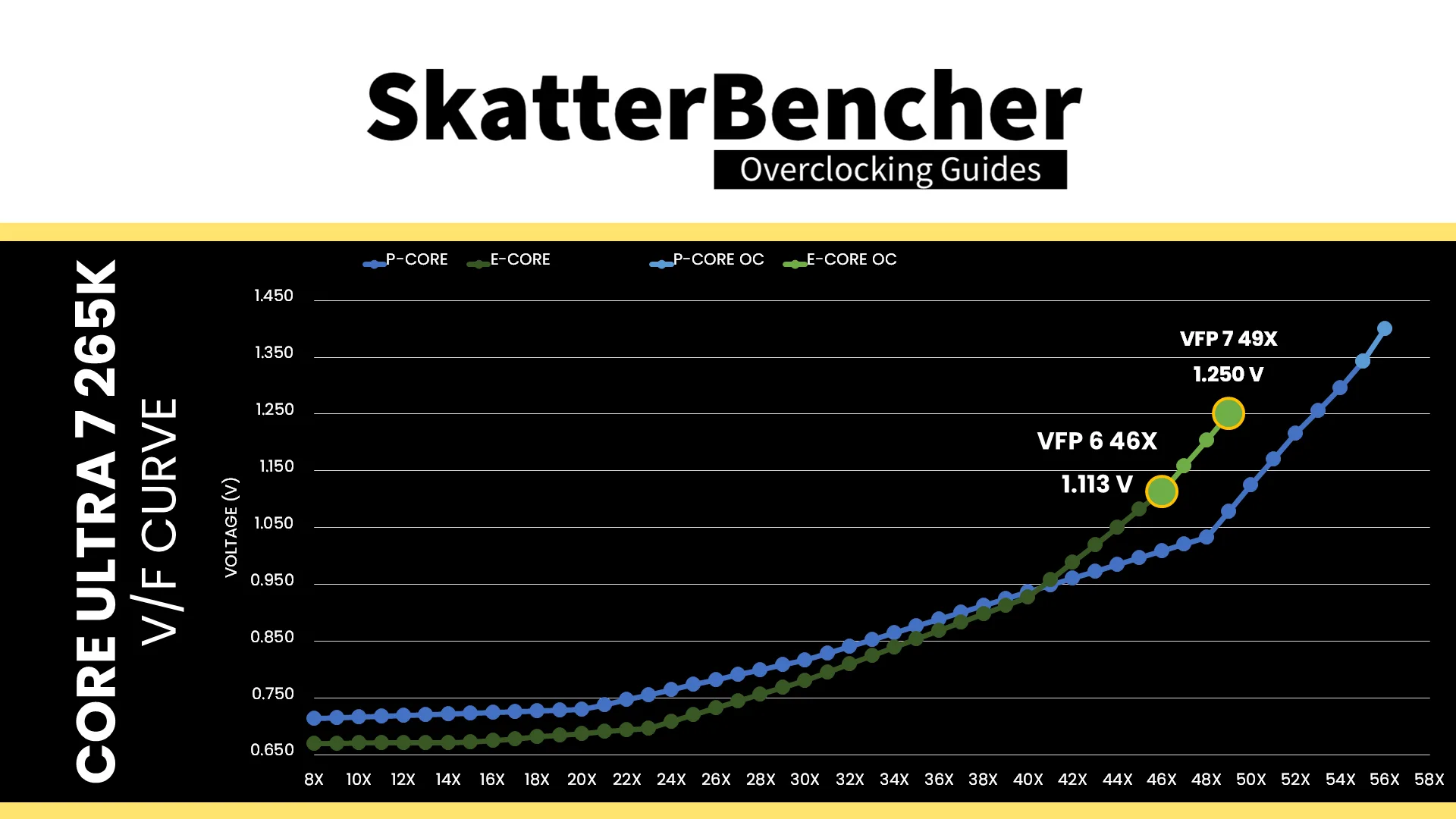
With 1.40V adaptive voltage for the P-cores, I could increase all P-cores to 5.6 GHz. However, in all core loads the maximum frequency was 5.5 GHz. With 1.25V adaptive voltage for the E-cores, I could increase all E-core clusters to 4.9 GHz. However, again, I had to drop the all-core frequency by 100 MHz to 4.8 GHz.
BIOS Settings & Benchmark Results
Upon entering the BIOS
- Go to the Ai Tweaker menu
- Set Performance Preferences to ASUS Advanced OC Profile
- Set Ai Overclock Tuner to XMP I
- Set ASUS MultiCore Enhancement to Enabled – Remove All Limits
- Set Performance Core Ratio to By Core Usage
- Set 1-Core to 4-Core Ratio Limit to 56
- Set 5-Core to 8-Core Ratio Limit to 55
- Set Efficient Core Ratio to By Core Usage
- Enter the By E-Core Usage submenu
- Set Efficient Turbo Ratio Limit 1 to 49
- Set Efficient Turbo Ratio Cores 1 to 6
- Set Efficient Turbo Ratio Limit 2 to 48
- Set Efficient Turbo Ratio Cores 2 to 12
- Leave the By E-Core Usage submenu
- Enter the Thermal Velocity Boost submenu
- Set TVB Voltage Optimizations to Disabled
- Set Enhanced TVB to Disabled
- Set Overclocking TVB to Disabled
- Leave the Thermal Velocity Boost submenu
- Enter the Max Voltage Limits submenu
- Set P-Core Max Voltage Limits to 1.45
- Set E-Core Max Voltage Limits to 1.30
- Leave the Max Voltage Limits submenu
- Enter the Performance Core V/F Point Offset submenu
- Set V/F Point Present Mode to All Core Mode
- Set V/F Point Voltage Control Mode to Manual Mode
- Leave the Performance Core V/F Point Offset submenu
- Enter the Efficient Core V/F Point Offset submenu
- Set V/F Point Present Mode to All Core Mode
- Set V/F Point Voltage Control Mode to Manual Mode
- Leave the Efficient Core V/F Point Offset submenu
- Set NGU Ratio to 32
- Set CPU D2D Ratio to 32
- Set Performance Core DLVR Voltage to Adaptive Mode
- Set Additional Turbo mode Voltage to 1.400
- Set Efficient Core DLVR Voltage to Adaptive Mode
- Set Additional Turbo mode Voltage to 1.250
- Set CPU System Agent Voltage to Manual Mode
- Set CPU System Agent Voltage Override to 1.200
Then save and exit the BIOS.
The CPU boost frequency with 1 active P-core is 5600 MHZ. The average boost frequency gradually trails off to 5500 MHz when all P-cores are active and to 5080 MHz when all P- and E-cores are active. In single-threaded applications, all P-cores can boost to 5.6 and all E-core clusters can boost to 4.9 GHz.
We re-ran the benchmarks and checked the performance increase compared to the default operation.

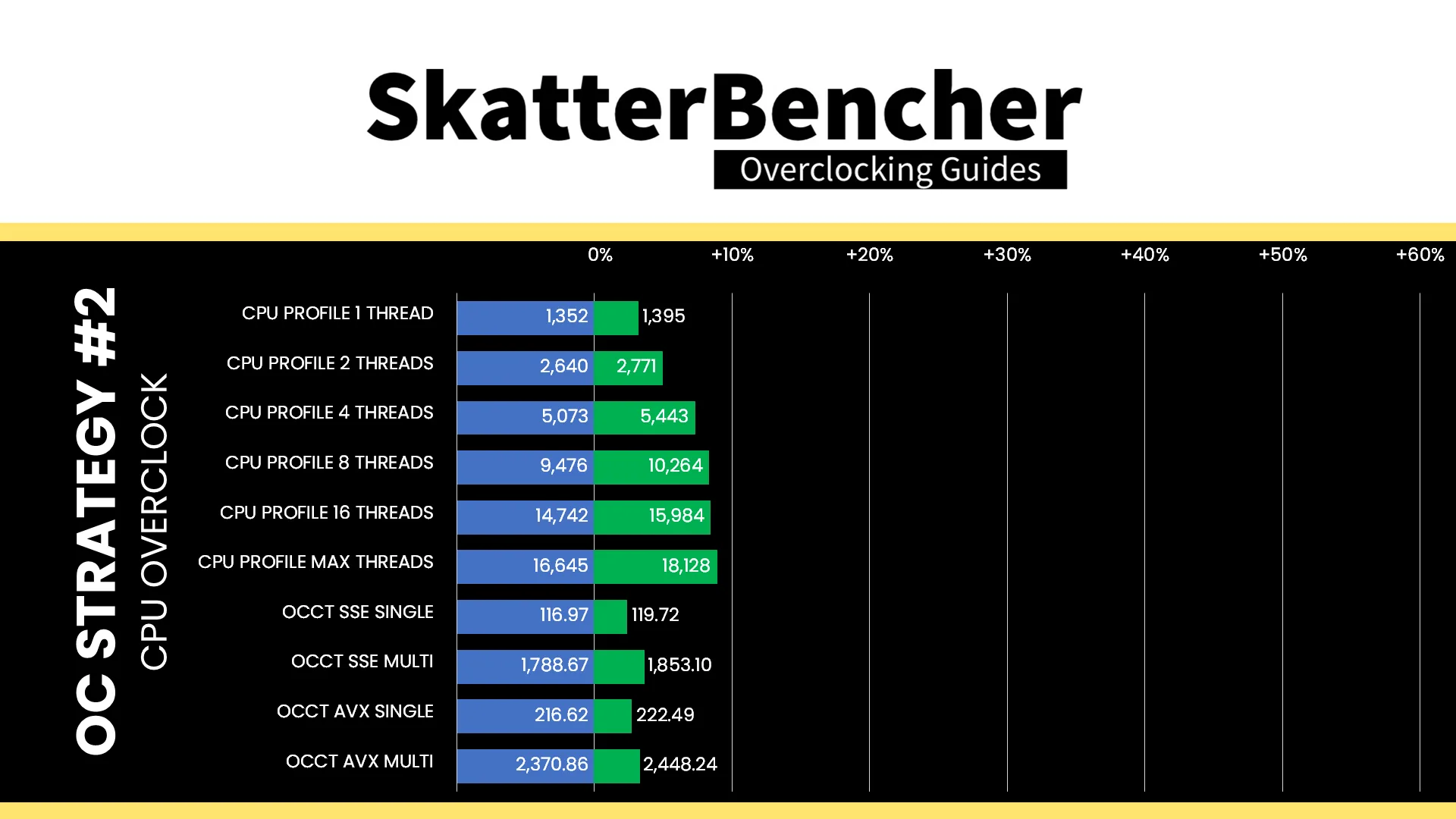

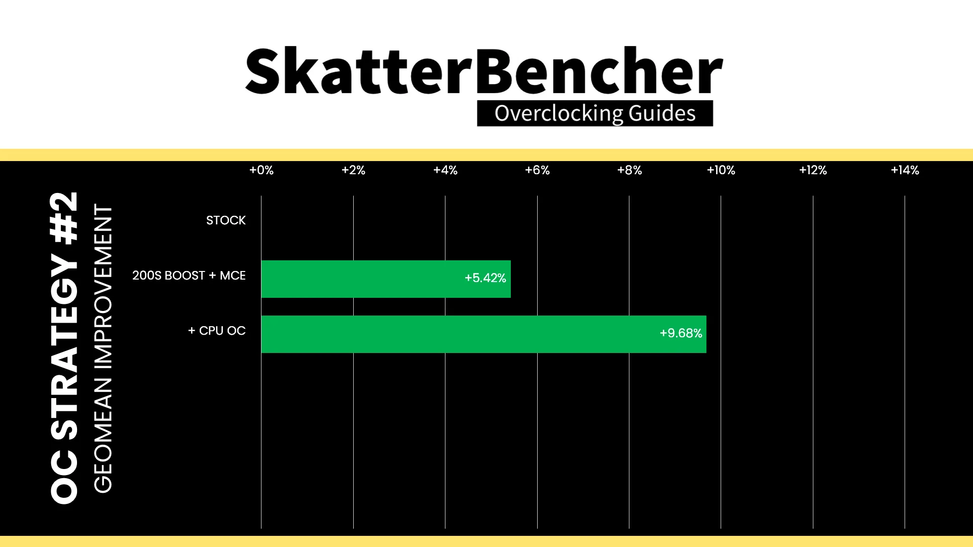
While the P-core overclocking headroom is very limited, we are able to squeeze it for an extra 300 MHz in all core workloads. We can also squeeze the E-cores for a couple hundred MHz extra frequency. The Geomean performance improves by another 4.26 percentage points, and we get a maximum improvement of +27.08% in PyPrime.
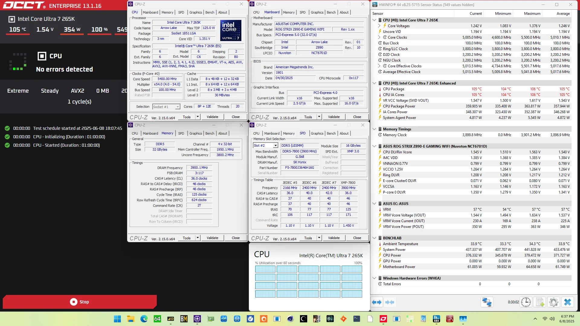
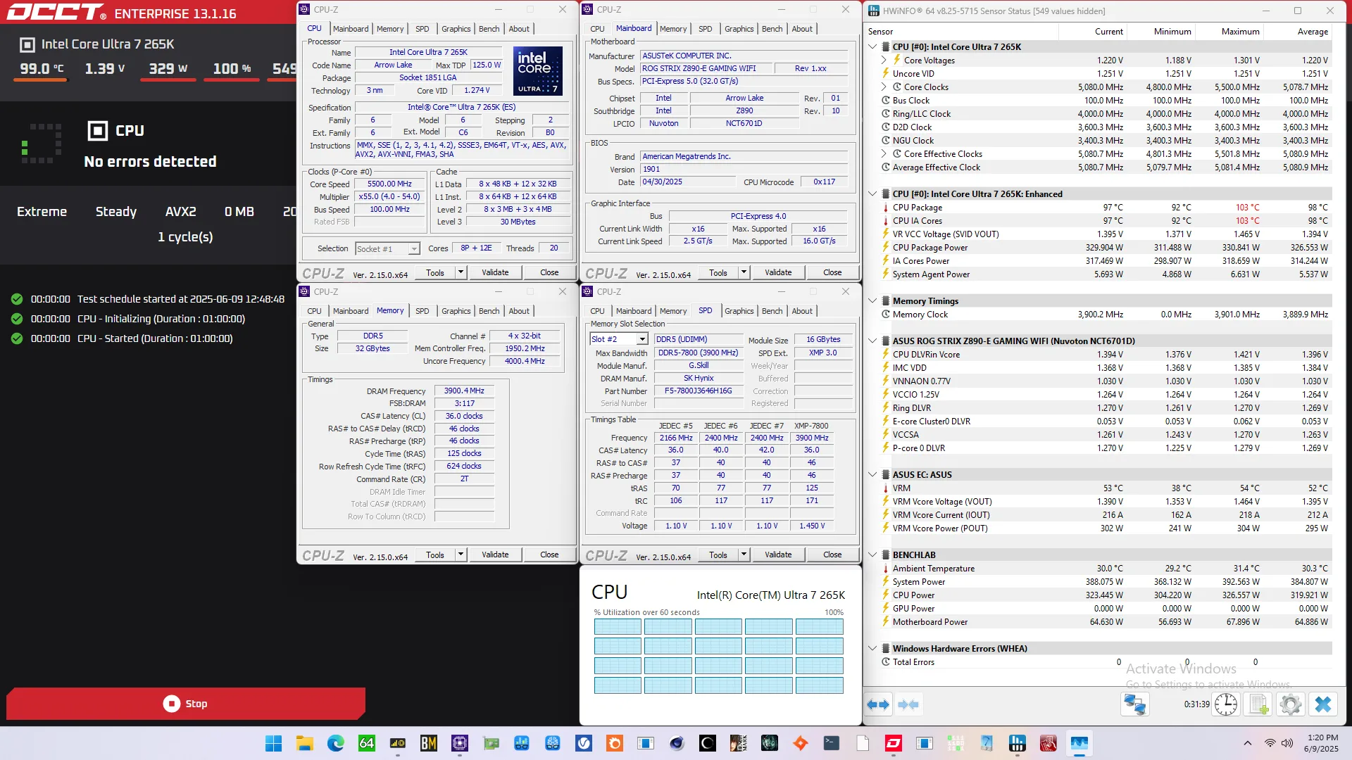
When running the OCCT CPU AVX2 Stability Test, the average CPU P-core effective clock is 5350 MHz with 1.341 volts and the average CPU E-core effective clock is 4795 MHz with 1.203 volts. The average CPU temperature is 105.0 degrees Celsius. The average CPU package power is 357.9 watts.
When running the OCCT CPU SSE Stability Test, the average CPU P-core effective clock is 5485 MHz with 1.342 volts and the average CPU E-core effective clock is 4792 MHz with 1.194 volts. The average CPU temperature is 103.0 degrees Celsius. The average CPU package power is 342.8 watts.

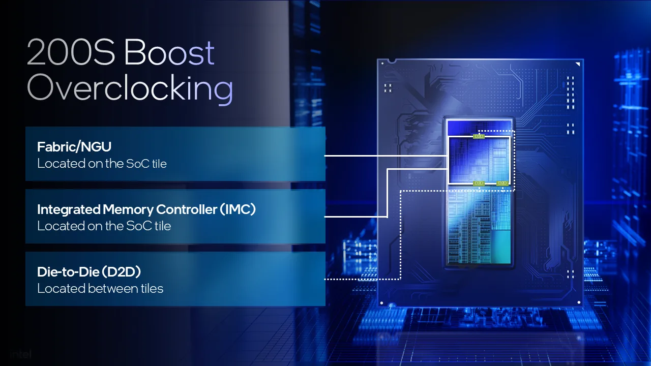
OC Strategy #3: Data Fabric Tuning
In our third overclocking strategy, we delve into tuning the data fabric which consists of the Ring, the NoC in the NGU, and the CPU D2D interface.
Ring
The Ring fabric provides the data fabric interface between the various Compute IP blocks in the Compute Tile, the last-level cache, and the SOC-Compute D2D interface.
Ring Clocking Topology
The Ring reference clock frequency is generated internally by the CPU PLL. This clock affects all IP blocks in the Compute Tile, including the P-cores, E-cores, and Ring. This PLL can be linked to the SoC PLL when you run in synchronous mode or work independently if you run in asynchronous mode.
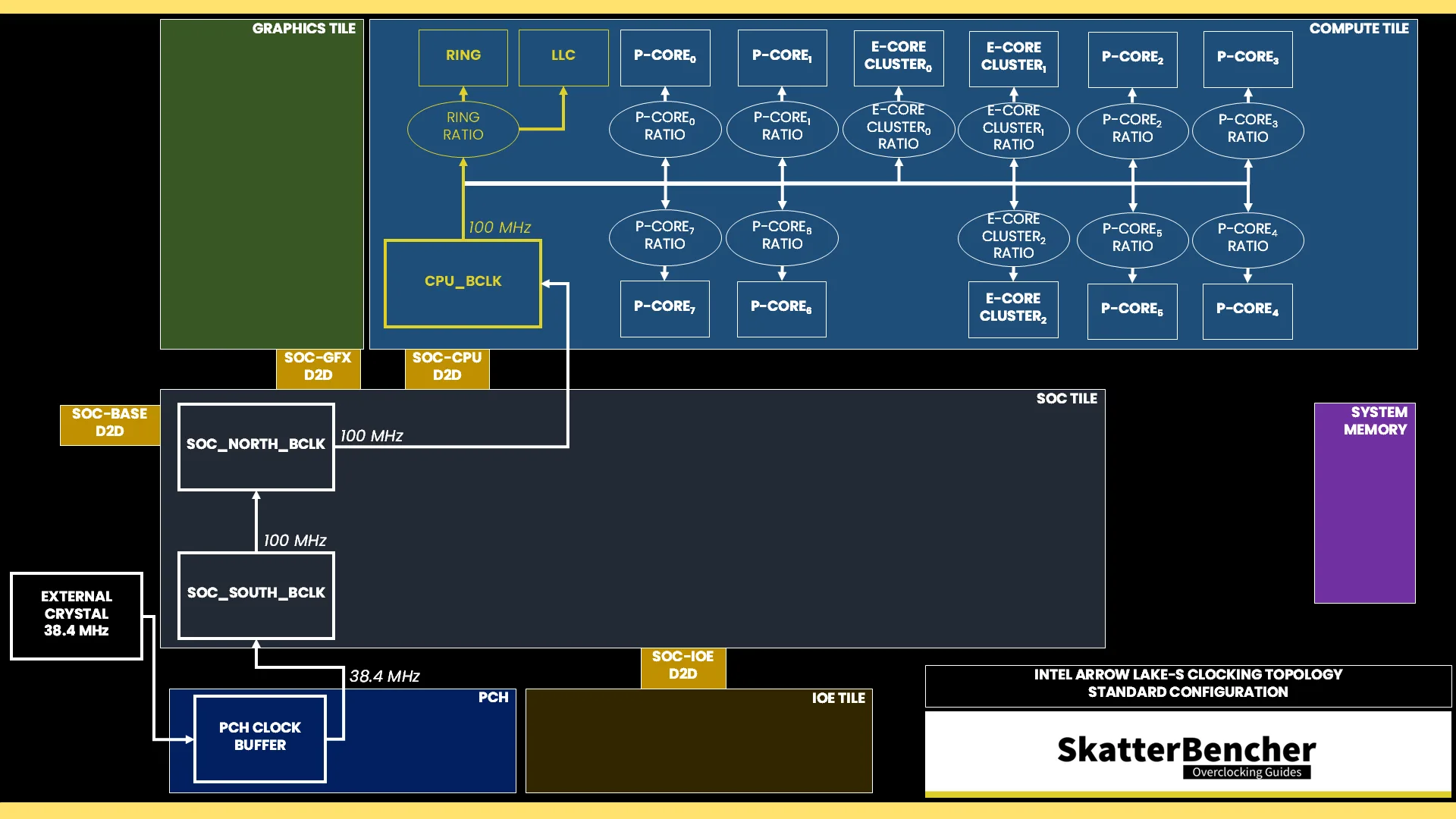
The reference clock is multiplied by the Ring ratio to achieve the final clock frequency. It operates independently from the P-cores and the E-cores. The default ratio is 38X, which yields a 3.8 GHz operating frequency.
Ring Voltage Topology
The voltage regulation for the Ring is more complex than prior generations of Intel Core processors due to the introduction of the DLVR. The DLVR enables much lower voltage levels for the Ring but still relies on a dynamic external motherboard voltage regulator as the input voltage source.
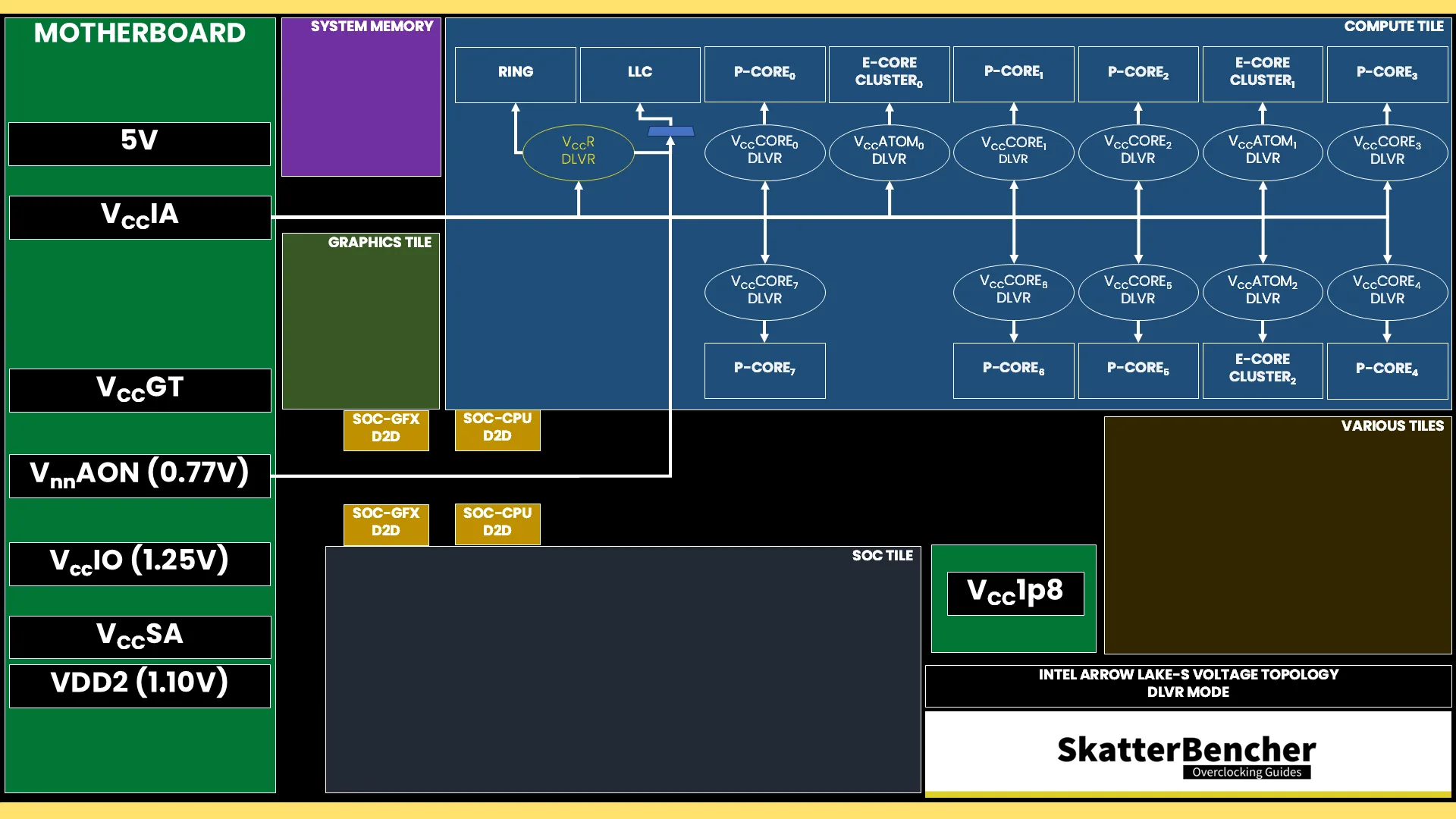
As we discussed earlier in the guide, the external VccIA motherboard voltage regulator (MBVR) provides the input voltage for DLVRs of the individual P-core, E-core clusters, Ring, last-level cache (LLC), and E-core L2 cache.
- VccCOREn is the DLVR powering an individual P-core.
- VccR is the DLVR powering the Ring and Last-Level Cache.
- VccATOMn is the DLVR powering an individual E-core cluster, which consists of four E-cores, and its L2 cache.
The DLVRs can also be bypassed. In that case, the IP blocks are running in so-called Power Gate (PG) mode.
V/F Curve
The Core Ultra 7 265K Ring has its own V/F curve which is defined by up to nine (9) V/F points. The first eight (8) V/F points are factory-fused, and the last point is mapped to the “OC Ratio.” Oddly enough, while the default Ring frequency is 3.8 GHz, the V/F curve is actually defined up to 3.9 GHz!
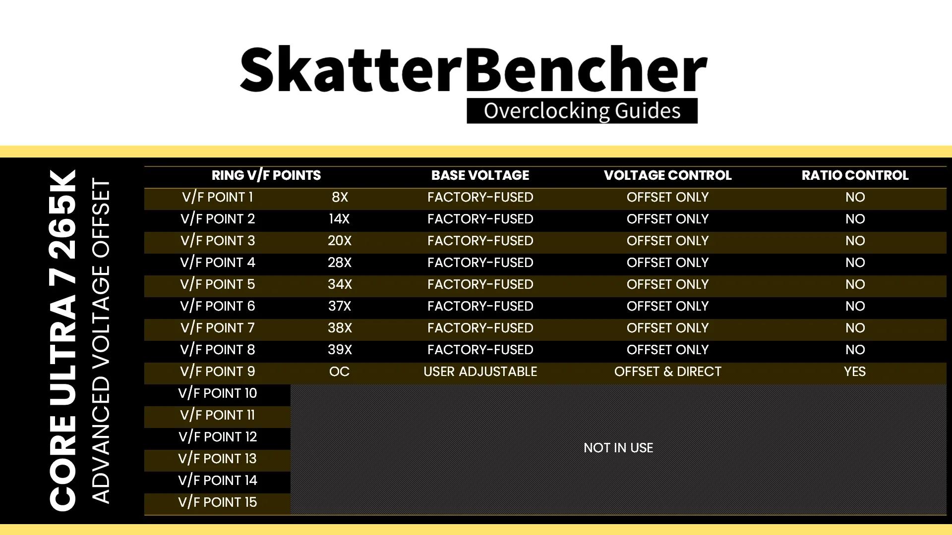
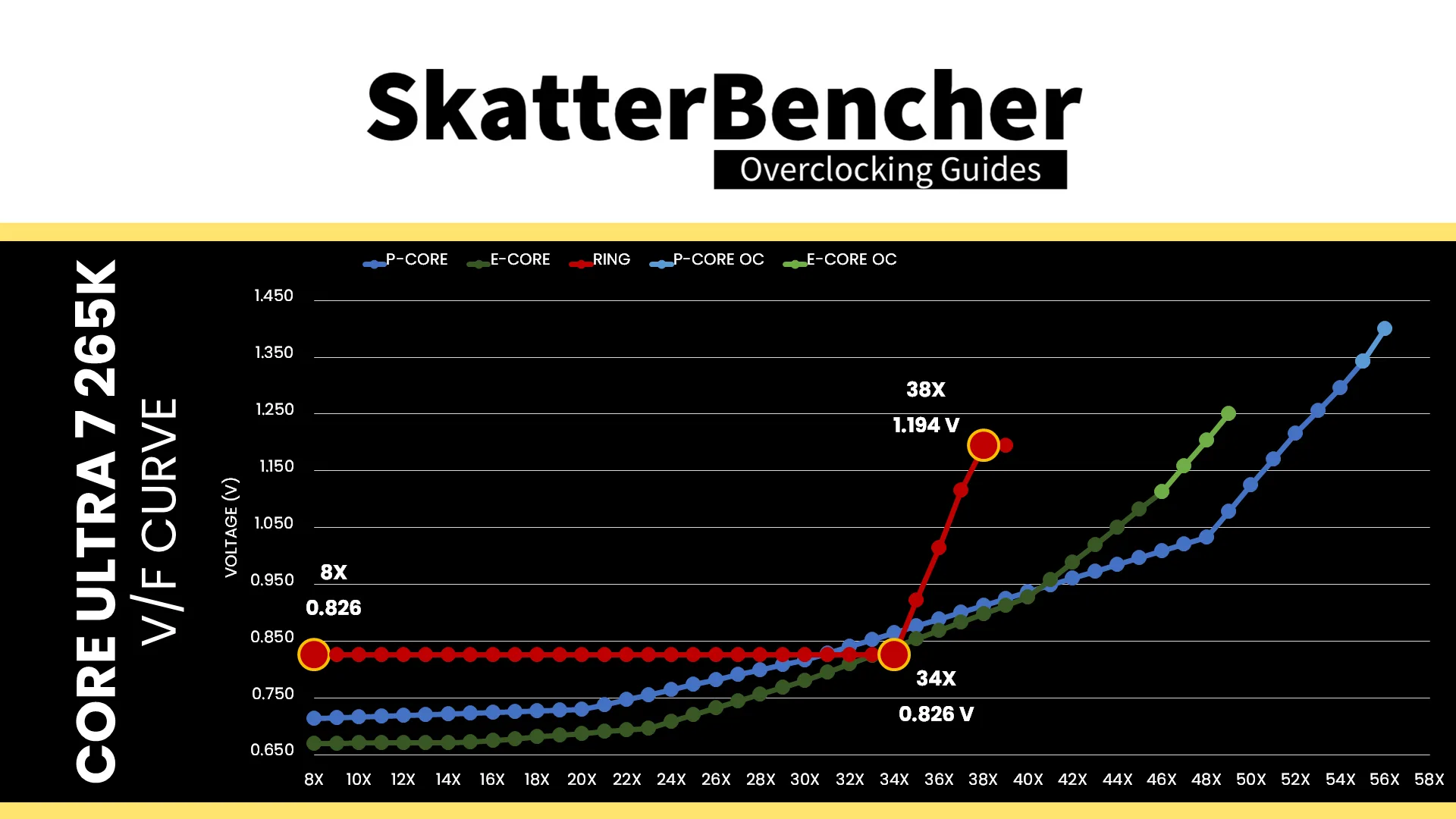
Here is the Ring V/F curve for my specific Core Ultra 7 265K. The voltage is about 826 mV at 800 MHz all the way up to 3.4 GHz, then increases nearly linearly to 1.194V for VF Point 7 at 3.8 GHz.
Adaptive Voltage Mode
Similar to the P-cores and E-cores, the Ring requests an operating voltage using the SVID protocol from the CPU Power Control Unit (PCU) based on its VF curve. The PCU in turn configures the VccIA voltage rail and the individual DLVRs.
The voltage configuration of the Ring is identical to that of the P-cores, including the Adaptive and Override modes, and the specific rules governing the adaptive voltage mode which I covered at length in the previous OC Strategy.
NGU / NoC
NGU stands for “Next Generation Uncore” and is the successor to the uncore we know from previous generation Intel processors. The NGU fabric – sometimes called sub-system – includes several subcomponents such as the network on chip (NoC) and UFI bridges. It’s located on the SoC tile.
On Arrow Lake-S, NGU overclocking is essentially NoC overclocking. The NOC fabric is the primary communication bridge between the various IP blocks on the chip such as the memory controller, the CPU cores (via D2D), graphics (via D2D), and so on.
NGU Clocking Topology
The NGU reference clock frequency is generated internally by the SoC PLL. However, it can also be clocked with an external clock generator providing the reference clock for the SoC PLL. This clock affects nearly all the IP blocks of Arrow Lake, except for those in the Compute Tile and the PCIe/DMI links.
The reference clock is multiplied by the NGU ratio to achieve the final clock frequency. The default ratio is 26X, which yields a 2.6 GHz operating frequency.
NGU Voltage Topology
The external VccSA MBVR powers several parts of the SOC dielet, including the NGU. Unlike Compute IP, the parts of the SOC dielet are not powered using DLVR. So, power delivery is identical to previous architectures.
The most relevant parts powered by the VccSA voltage rail are the system agent, the NoC, the NPU, and the memory controller. The voltage configuration of the VccSA voltage rail is rather complicated. Since multiple IP domains share the voltage rail, the VccSA voltage is set based on the highest requested voltage from the various connected IP blocks.
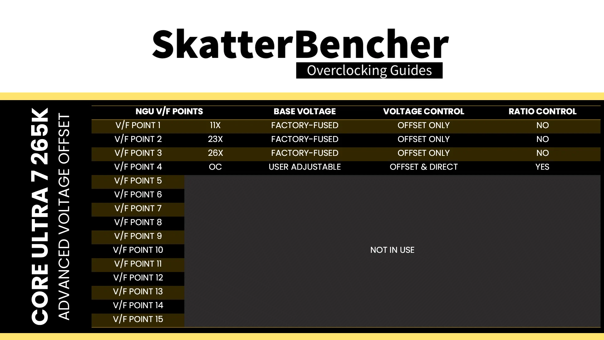
The NoC has its own V/F curve which is defined by up to four (4) V/F work points. The first three (3) V/F points (at 11X, 23X, and 26X) are factory-fused and the last point is mapped to the “OC Ratio.” Unfortunately, that’s as much as we can gather regarding the default V/F curve. It’s not easy to separate the NGU SVID request based on the VccSA behavior.
Based on the work points, the NGU requests an operating voltage from the VccSA voltage rail using the SVID protocol. However, there’s a second way to voltage configuration: ignore the SVID voltage requests and calculations, and program the VccSA voltage regulator directly over PMBus. This process effectively allows us to take full control over the voltage set by the VccSA voltage rail.
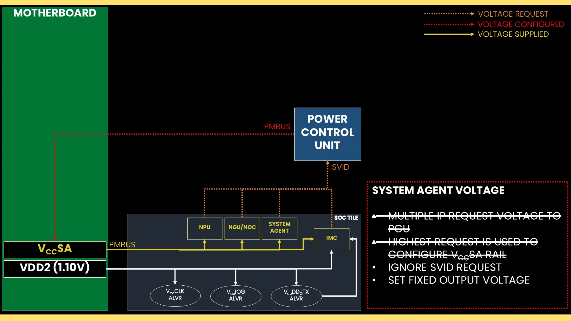
This approach is a very traditional way of overclocking whereby you set a fixed output voltage and then use an appropriate VRM load-line setting – if available – to reduce the operating voltage in higher load scenarios. The load-line configuration isn’t particularly useful for SA voltage rail.
D2D
D2D stands for Die-to-Die. It is the interface between the various tiles on the Arrow Lake package. There are three D2D links connecting the various tiles on the Arrow Lake package:
- SOC-Compute (H-IDI protocol) – P-core, E-core, Ring
- SOC-Graphics (CXL protocol) – Integrated Graphics
- SOC-IOE (PSF protocol) – IO extension
On Arrow Lake, only the SOC-Compute D2D can be overclocked. The base frequency is 2.1 GHz.
D2D Clocking Topology
The D2D reference clock frequency is generated internally by the SoC PLL. However, it can also be clocked with an external clock generator providing the reference clock for the SoC PLL. This clock affects nearly all the IP blocks of Arrow Lake, except for those in the Compute Tile and the PCIe/DMI links.
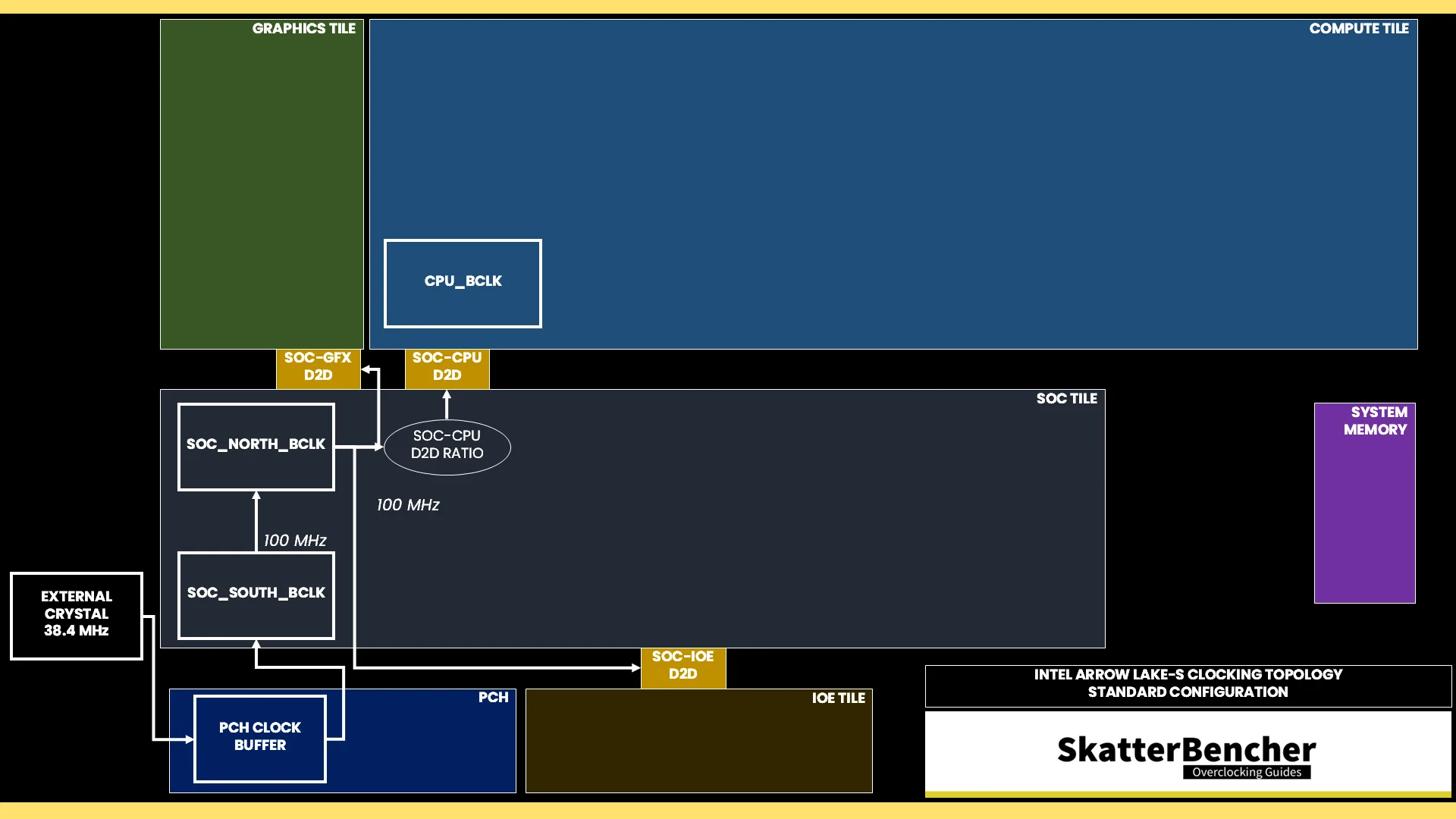
The reference clock is multiplied by the D2D ratio to achieve the final clock frequency. As said, we can only adjust the SOC-Compute D2D frequency. The default ratio is 21X, which yields a 2.1 GHz operating frequency. The maximum configurable ratio is 40X. The frequency can only be set at boot and cannot be changed in the operating system.
D2D Voltage Topology
The external 0.77V VnnAON voltage rail powers several internal voltages, including the D2D interfaces. The VnnAON voltage is pretty important for Arrow Lake CPUs as it is part of the voltage multiplexer for many IP blocks, including the cores and ring, typically serving as the floor voltage in power-saving scenarios.
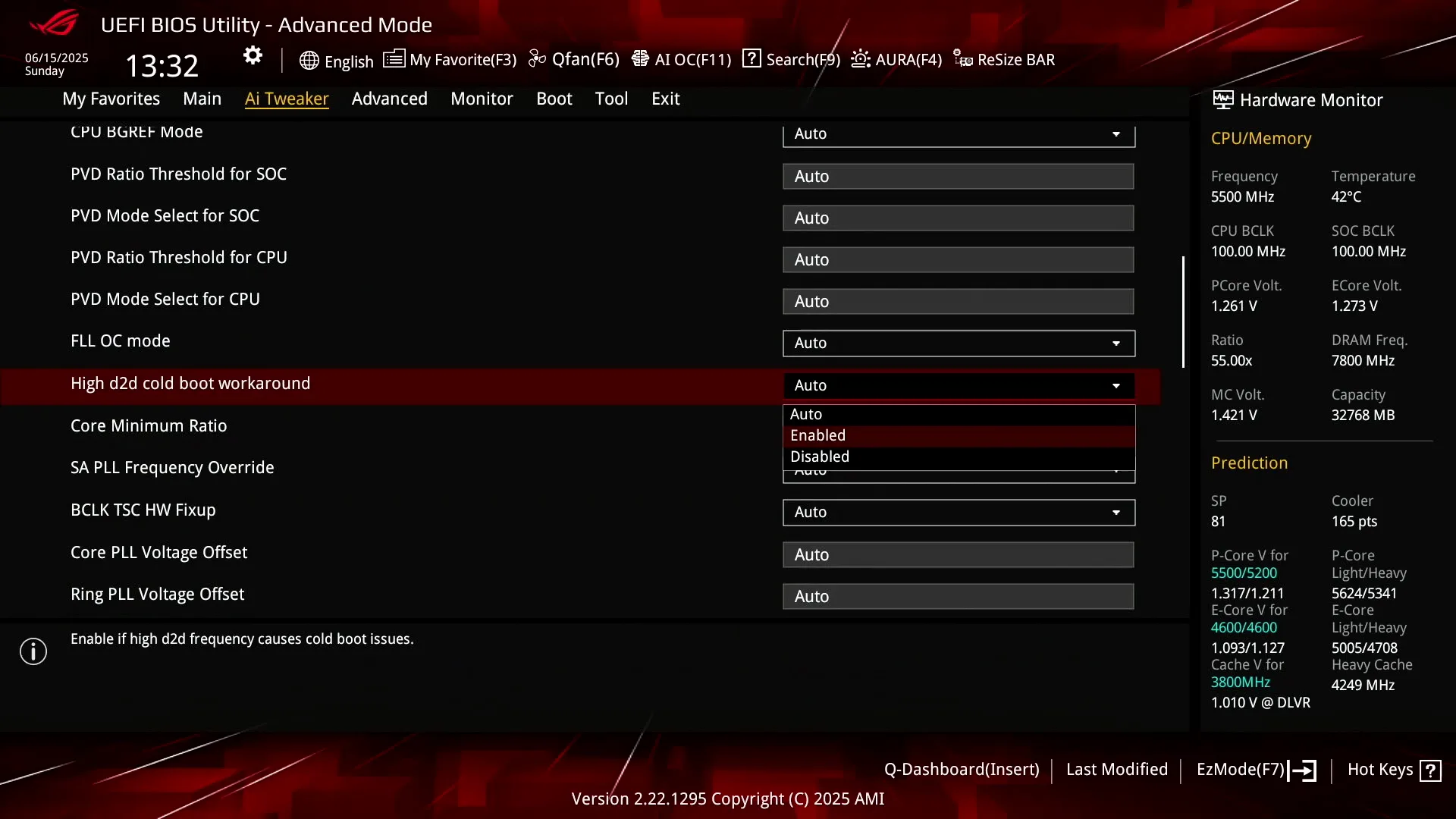
I don’t suggest increasing it above 1.0V since it provides little additional benefit for overclocking and performance. Furthermore, increasing the VnnAON voltage can also cause issues when cold booting the system. Fortunately, ASUS has included an option called “High d2d cold boot workaround” in the BIOS that can help alleviate some of the booting issues with increased VnnAON voltages.
Data Fabric Tuning Process
Tuning the data fabric is a matter of testing each component systematically. I recommend first picking target voltages for each of the components and setting those in the BIOS with each component set to its default frequency. So:
| Component | Default | Initial Config |
| Ring | 38X at 1.194 V | 38X at 1.250 V |
| NGU | 26X at 1.050 V | 26X at 1.300 V |
| D2D | 21X at 0.770 V | 21X at 1.000 V |
Then I increase the frequency for each component until I find instability. The initial tests can be very quick. For example, I’ll run a 30 second cycle of Y-Cruncher FFT Component tester to find the initial upper limit for each component.
| Component | Default | Initial Config | 1st Test | 2nd Test | 3rd Test |
| Ring | 38X at 1.194 V | 38X at 1.250 V | Increase Ring | 38X at 1.250 V | 38X at 1.250 V |
| NGU | 26X at 1.050 V | 26X at 1.300 V | 26X at 1.300 V | Increase NGU | 26X at 1.300 V |
| D2D | 21X at 0.770 V | 21X at 1.000 V | 21X at 1.000 V | 21X at 1.000 V | Increase D2D |
When I know the upper limit, I’ll set all target ratios and do longer stints of stability testing including the introduction of other tests. I find that, typically, Cinebench R23, Y-Cruncher Benchmark & Component Tester, and AI Benchmark are very sensitive to data fabric overclocking.
This process might take a bit longer, especially if you’re trying to find the maximum stable setting. When I’m satisfied with the stability testing, of course it also has to pass all the other benchmarks in our benchmark suite.
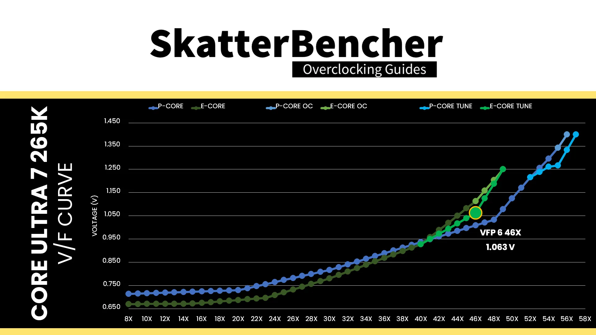
Ultimately, I ended up with a 4.0 GHz Ring, 3.4 GHz NGU, and 3.6 GHz D2D.
| Component | Default | Initial Config | Final Config |
| Ring | 38X at 1.076 V | 38X at 1.250 V | 40X at 1.250 V |
| NGU | 26X at 1.050 V | 26X at 1.300 V | 34X at 1.300 V |
| D2D | 21X at 0.770 V | 21X at 1.000 V | 36X at 1.000 V |
I want to emphasize a particular point regarding the Ring as I’ve received quite a number of questions about it. Don’t be surprised if you see extremely limited overclocking headroom for the Ring. It’s normal. For the 265K, 4.0 GHz is within expectations. For the 245K, the Ring can be clocked a little higher as I demonstrated in SkatterBencher #83.
BIOS Settings & Benchmark Results
Upon entering the BIOS
- Go to the Ai Tweaker menu
- Set Performance Preferences to ASUS Advanced OC Profile
- Set Ai Overclock Tuner to XMP I
- Set ASUS MultiCore Enhancement to Enabled – Remove All Limits
- Set Performance Core Ratio to By Core Usage
- Set 1-Core to 4-Core Ratio Limit to 56
- Set 5-Core to 8-Core Ratio Limit to 55
- Set Efficient Core Ratio to By Core Usage
- Enter the By E-Core Usage submenu
- Set Efficient Turbo Ratio Limit 1 to 49
- Set Efficient Turbo Ratio Cores 1 to 6
- Set Efficient Turbo Ratio Limit 2 to 48
- Set Efficient Turbo Ratio Cores 2 to 12
- Leave the By E-Core Usage submenu
- Enter the Thermal Velocity Boost submenu
- Set TVB Voltage Optimizations to Disabled
- Set Enhanced TVB to Disabled
- Set Overclocking TVB to Disabled
- Leave the Thermal Velocity Boost submenu
- Enter the Max Voltage Limits submenu
- Set P-Core Max Voltage Limits to 1.45
- Set E-Core Max Voltage Limits to 1.30
- Set Ring Max Voltage Limits to 1.30
- Leave the Max Voltage Limits submenu
- Enter the Performance Core V/F Point Offset submenu
- Set V/F Point Present Mode to All Core Mode
- Set V/F Point Voltage Control Mode to Manual Mode
- Leave the Performance Core V/F Point Offset submenu
- Enter the Efficient Core V/F Point Offset submenu
- Set V/F Point Present Mode to All Core Mode
- Set V/F Point Voltage Control Mode to Manual Mode
- Leave the Efficient Core V/F Point Offset submenu
- Enter the Tweaker’s Paradise submenu
- Set High d2d cold boot workaround to Enabled
- Leave the Tweaker’s Paradise submenu
- Set Max. CPU Cache Ratio to 40
- Set NGU Ratio to 34
- Set CPU D2D Ratio to 36
- Set Performance Core DLVR Voltage to Adaptive Mode
- Set Additional Turbo mode Voltage to 1.400
- Set Efficient Core DLVR Voltage to Adaptive Mode
- Set Additional Turbo mode Voltage to 1.250
- Set Ring DLVR Voltage to Adaptive Mode
- Set Additional Turbo mode Voltage to 1.200
- Set CPU System Agent Voltage to Manual Mode
- Set CPU System Agent Voltage Override to 1.300
- Set VNNAON 0.77v Voltage to Manual Mode
- Set VNNAON Voltage Override to 1.000
Then save and exit the BIOS.
We re-ran the benchmarks and checked the performance increase compared to the default operation.
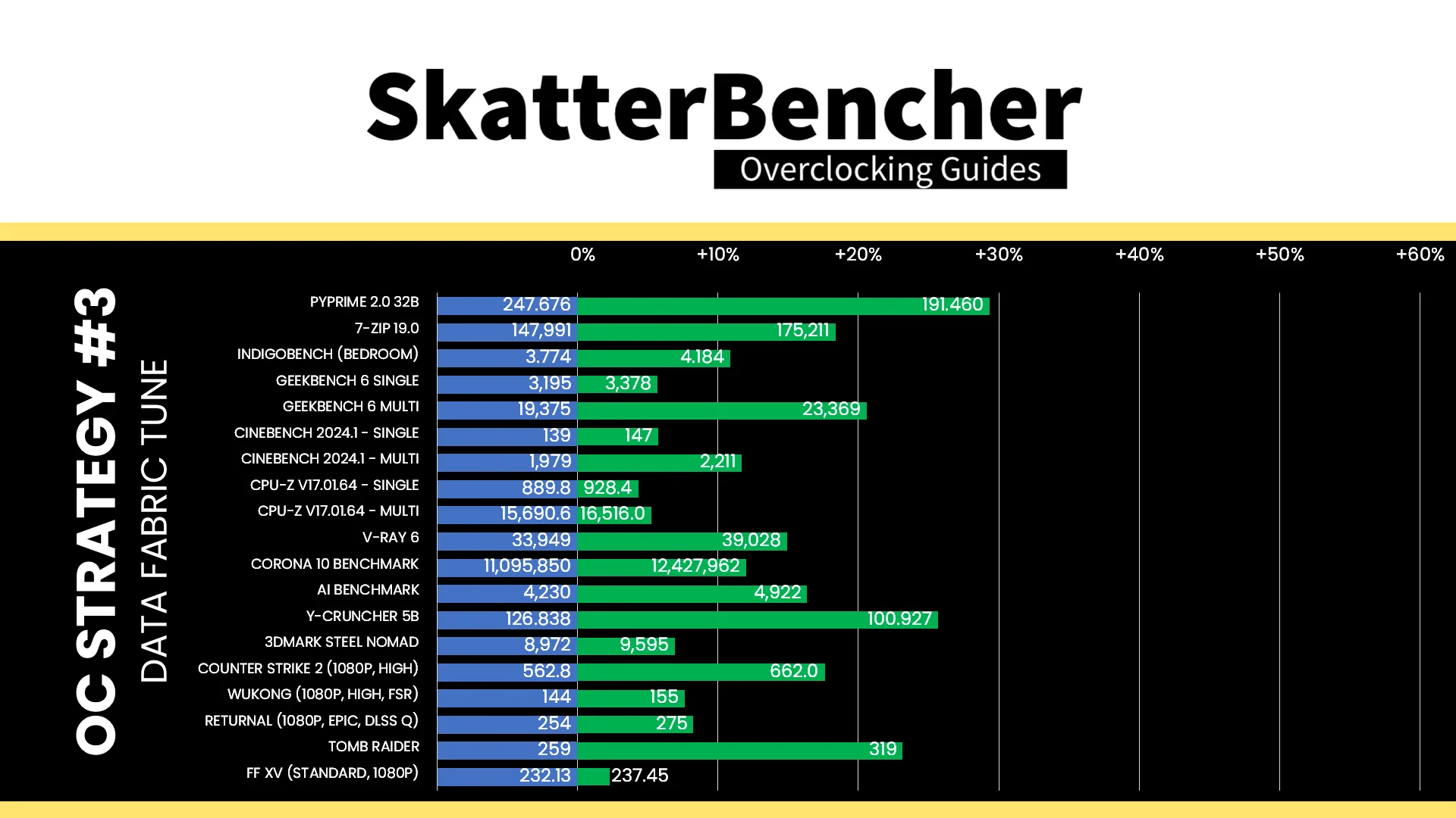
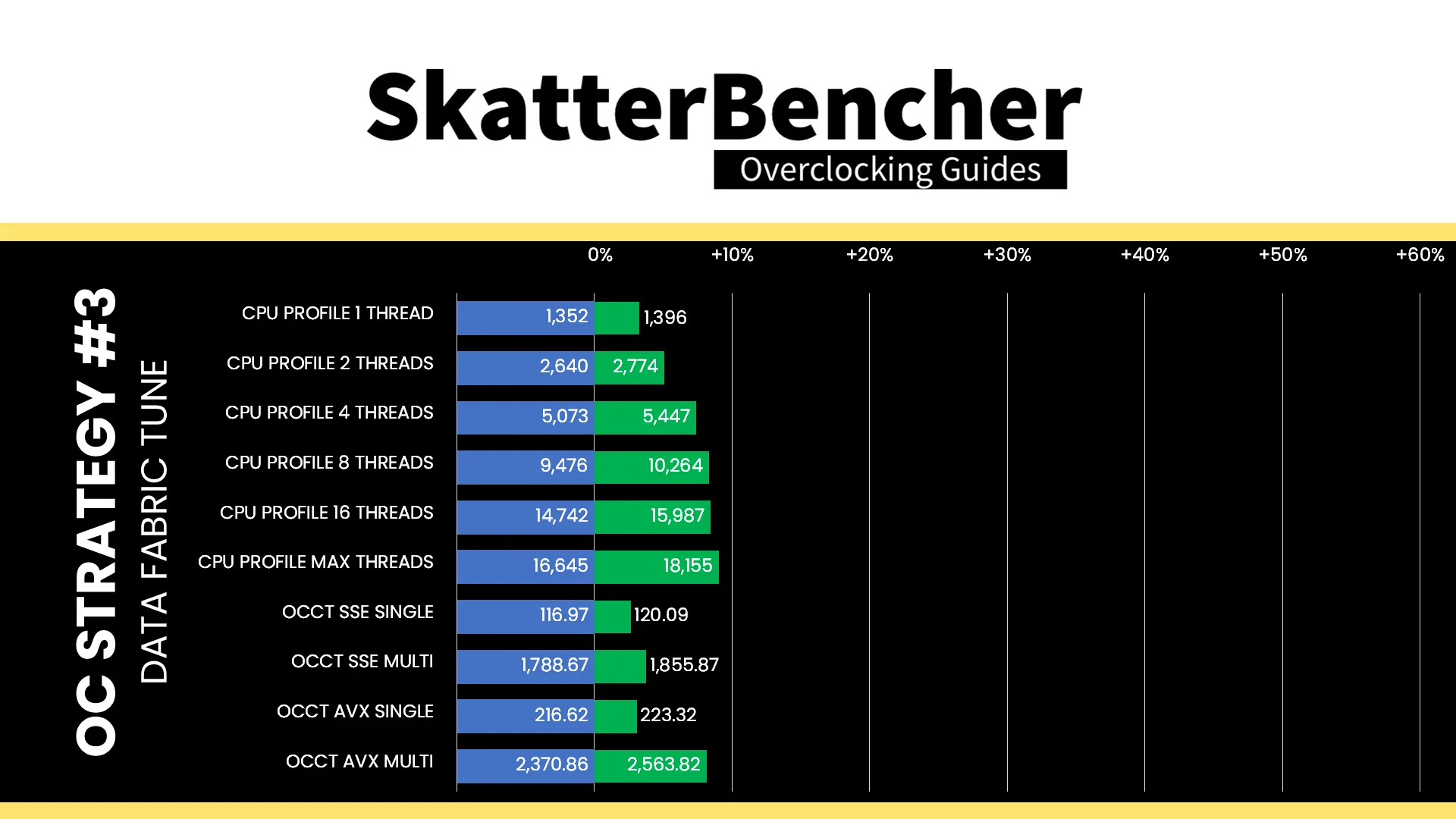
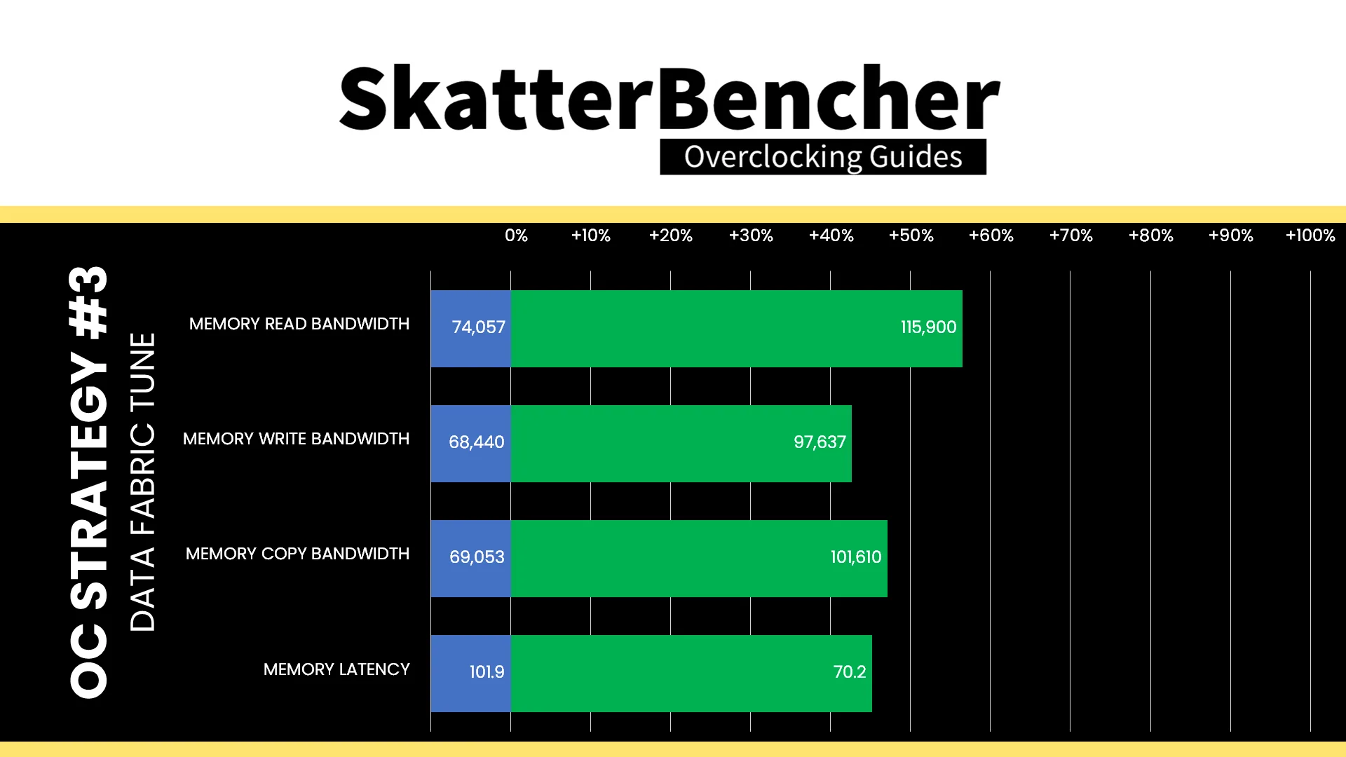
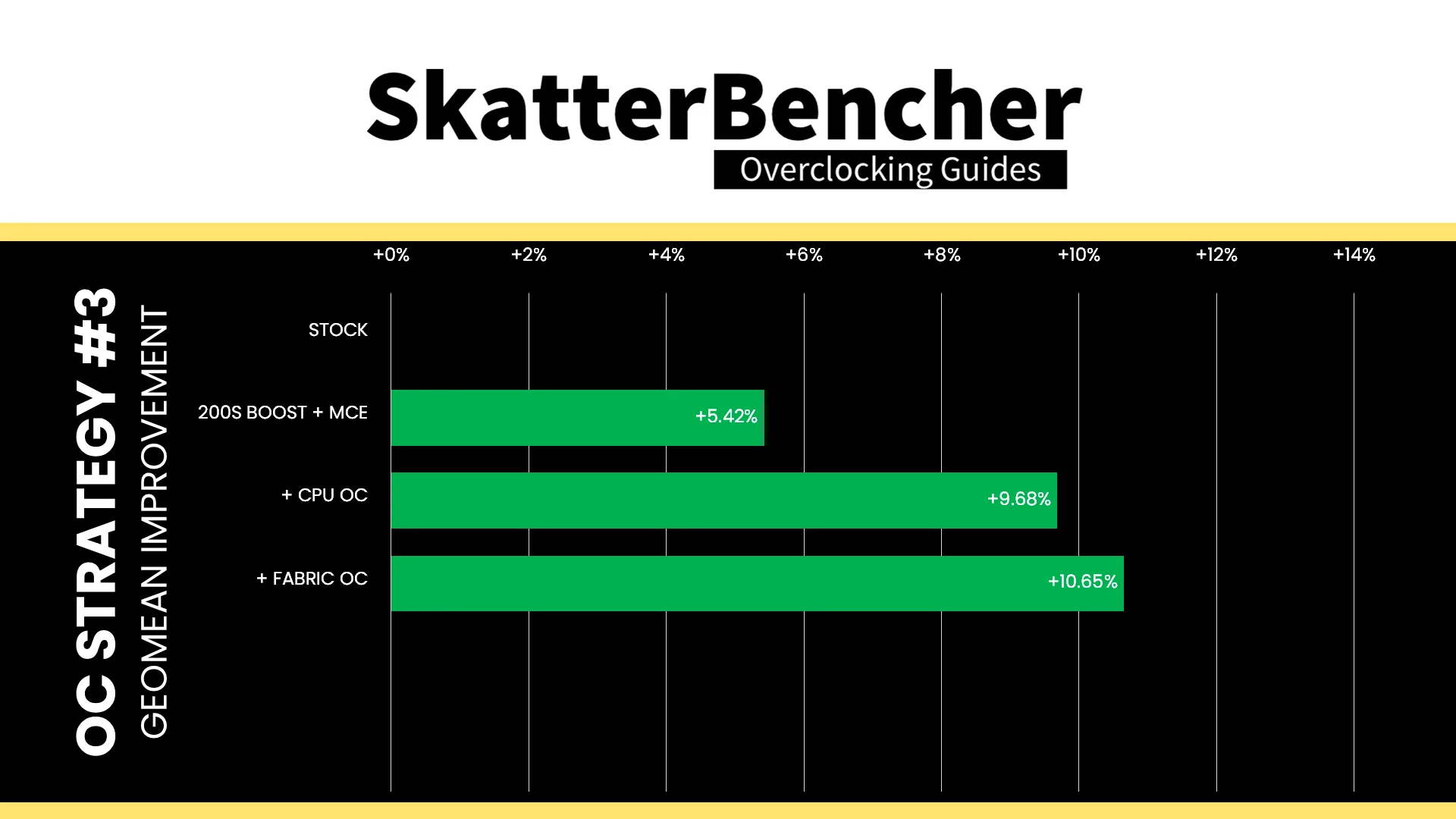
The multi-tile Arrow Lake architecture adds some layers of communication between the system memory and CPU cores. By increasing the frequency of the Ring, NGU, and D2D, we aim to increase the data transfer speed. Most of the heavy lifting was already done with 200S Boost, so further tuning only gets us a minor performance improvement. The Geomean performance improves by another percentage point, and we get a maximum improvement of +29.36% in PyPrime.
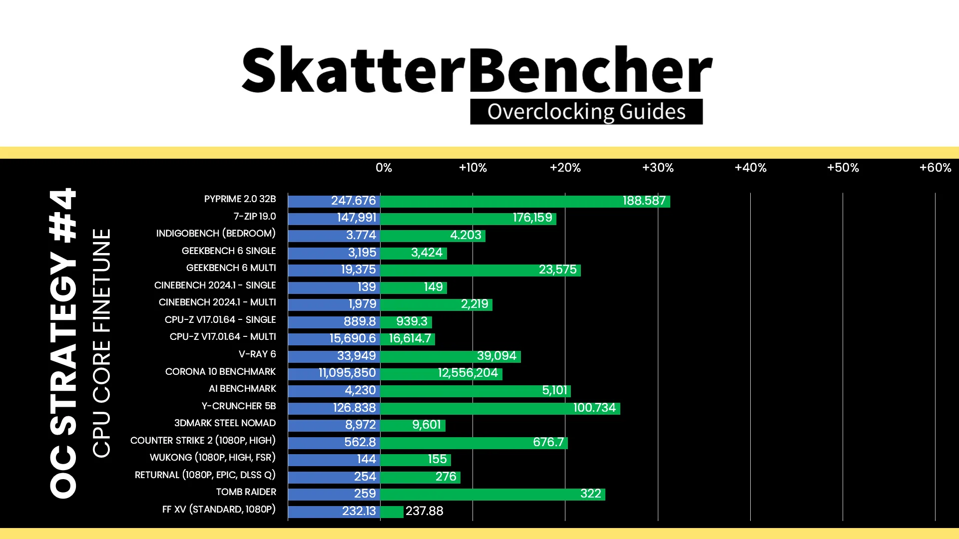
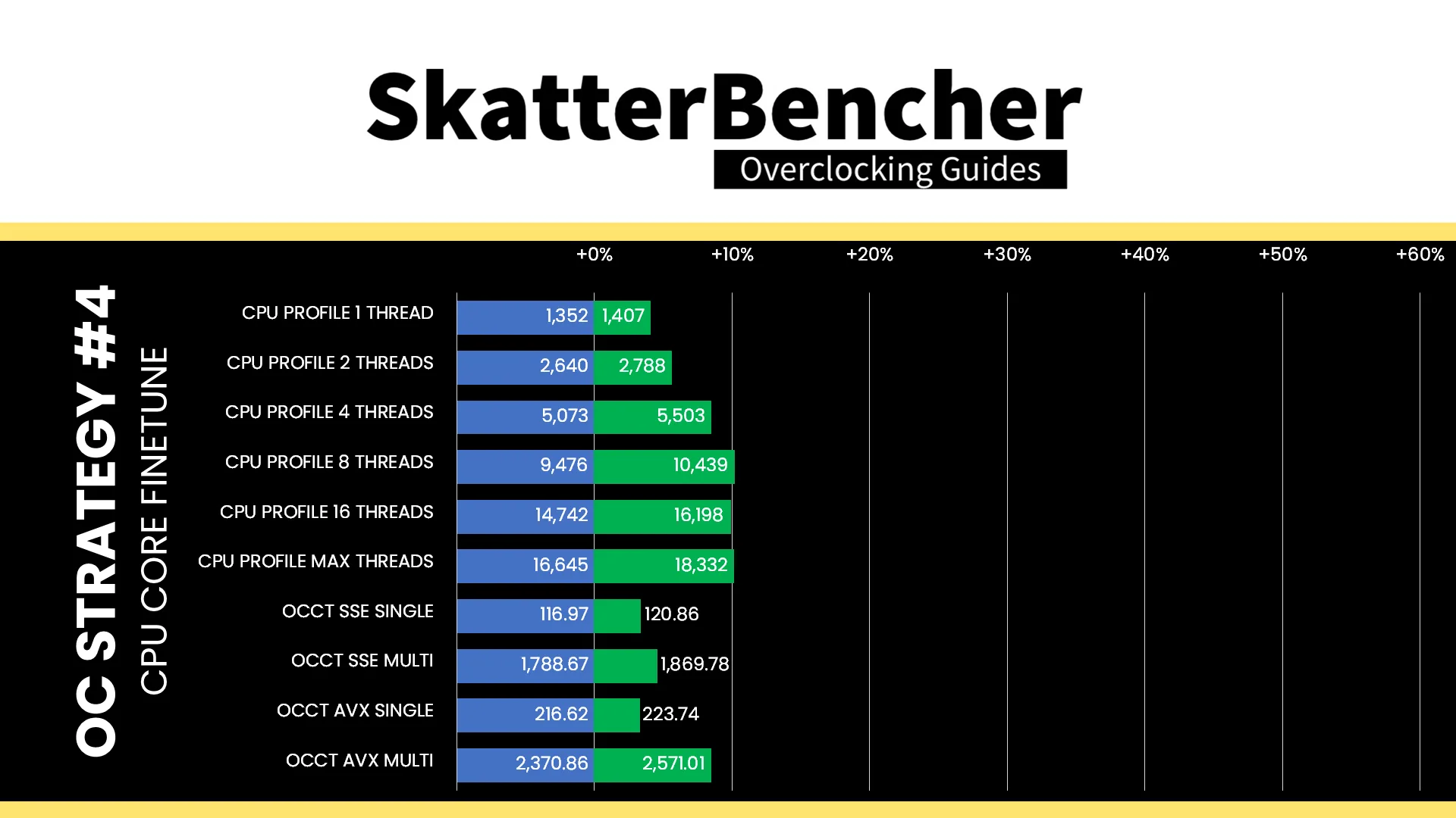
OC Strategy #4: CPU Core Finetuning
In our fourth overclocking strategy, I try to squeeze more performance out of the CPU cores by exploring the advanced tuning technologies available for Arrow Lake. That includes overclocking thermal velocity boost and advanced voltage offset.
OverClocking Thermal Velocity Boost
Intel OverClocking Thermal Velocity Boost (OCTVB) reduces the CPU core ratio at specified operating temperatures. While OCTVB is not new for Arrow Lake, the feature has expanded in functionality because we can now configure the OCTVB based on the “Per CCP Module” or “Per P-core Group.”
Perhaps an easier way to think about this is that the former adjusts the Per Core Ratio Limit, and the latter adjusts the Turbo Ratio Limit. The latter is functionality carried over from previous generations whereas the former is new for Arrow Lake.
- In “Per CCP Module” mode, each P-core Per Core Ratio Limit has two available OCTVB points. Each point is defined by a target temperature and a number of down-bins.
- In “Per P-core Group” mode, each P-core Turbo Ratio Limit scenario has two available OCTVB points, each of which is defined by a target temperature and a number of down-bins.
For any OCTVB point, the temperature can be defined anywhere between 1 and 115 degrees Celsius. The down-bins can be defined between 0 and 31. Note that the down-bins are cumulative and thus the down-bins from point B stack on top of the down-bins from point A.
For example, let’s say we’ve set the Turbo Ratio Limit for 2 active P-cores to 60X, and set the “Per P-core Group” OCTVB Point A to -2X at 50C and OCTVB Point B to -2X at 80C. In that case, when 2 P-cores are active, the frequency will be 6 GHz below 50C, 5.8 GHz between 50C and 80C, and 5.6 GHz above 80C.
One last important thing to mention is that, for now at least, the temperature point is 5C off. By that, I mean that if you set the OCTVB point to 55C it actually kicks in at 60 degrees. That may be due to the TjMax increase from 100C on the previous generation Raptor Lake to 105C on Arrow Lake.
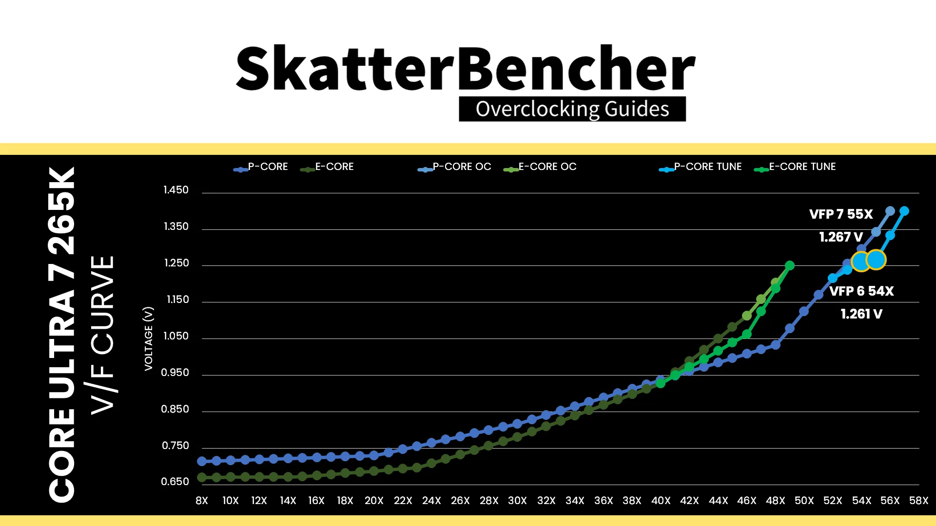
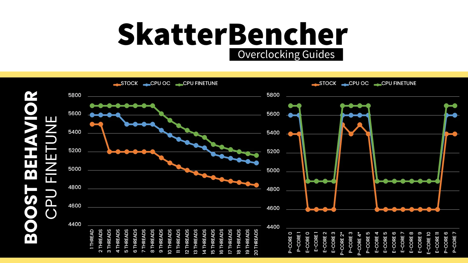
In practice, this tool is very helpful in managing instabilities at high frequencies in all core workloads and can help eek out extra boost at low temperatures. Specifically, for this 265K, I found that the P-cores can run at 5.7 GHz below 60 degrees Celsius and 5.6 GHz in light all-core workloads.
So, I configure the P-cores to run at 5.7 GHz when any number of cores are active, but down-bin by -1 at 60 degrees Celsius. For more than 5 active P-cores, I further down-bin another step at 80 degrees Celsius. Effectively, that gives me another 100 MHz boost in light workloads compared to the previous OC Strategy.
Advanced Voltage Offset
Advanced Voltage Offset, more commonly known as V/F Points, is available for each of the P-cores and each of the E-core clusters. There are eight (8) available VF Points for each P-core, seven of which are fixed to a specific ratio. That ratio is the same for all P-cores. There are seven (7) available VF Points for each E-core cluster, six of which are fixed to a specific ratio. That ratio is the same for all E-core clusters.
The final VF Point is mapped to the “OC Ratio” which is the P-core or E-core Cluster Per Core Ratio Limit. If you use granular ratios, keep in mind those are down-binned from the next full ratio. In other words, the OC Ratio cannot be a granular ratio!
You can set a negative or positive voltage offset for each of these V/F points. The final OC ratio’s base voltage will be the user-configured adaptive voltage. I’ll cover how I tuned the V/F Points in a minute.
VccIA MBVR
As we discussed a couple times already in this guide, external VccIA motherboard voltage regulator (MBVR) provides the input voltage for the VccCOREn, VccATOMn, and the VccR DLVRs.
It is a dynamic voltage that’s configured by the CPU PCU based on the voltage requests from all the different IP blocks powered by these DLVRs. However, we can also manually override the VccIA voltage while maintaining DLVR mode. I decided for this OC Strategy to try a static VccIA voltage mode for two reasons.
- With the elevated voltages, the VccIA maximum voltage jumps up quite a bit over 1.6 V.
- I found that the system stability was more predictable, making it easier to eke out additional frequency.
Since the maximum voltage for the VccIA-powered DLVRs is 1.40V (P-cores), I settled on a static VccIA voltage of 1.50 V. Do note that you must also consider the VccIA VR load-line, just like with previous architectures. I fixed the load-line to level 6 to have a flatter curve across all loads.
Arrow Lake P-core and E-core Finetuning Discussion
Based on my experience with Arrow Lake overclocking with the Core Ultra 5 245K and Core Ultra 9 285K, I don’t expect the P-cores to scale very much with additional voltage. So, instead, I wanted to focus on undervolting the P-core and E-core V/F curve to achieve higher boost in high-load scenarios.
The main objective is to get the P-cores to run at 5.5 GHz in the OCCT AVX2 workload, up 150 MHz from the temperature-throttled 5350 MHz we got in OC Strategy #2. To achieve this, we can look at both the P-core and E-core V/F curves.
P-core Undervolting
For the P-cores, I turn to V/F Points 6 and 7 which map to ratios 54X and 55X respectively. The goal is to reduce the voltage at 5.5 GHz so we avoid thermal throttling.
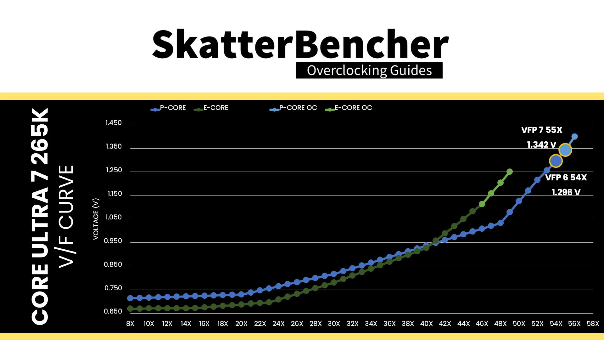
V/F Point 7 maps to the 55X ratio so it’s the obvious candidate for undervolting. However, make sure to keep in mind the adaptive voltage rules: the voltage for 55X cannot be lower than the voltage for 54X. Based on the V/F curve, we know that there’s only about 40 mV difference between the two V/F points. So, unless we also undervolt V/F Point 6, the undervolt margin for 55X is limited to 40 mV.
In my case, I undervolt V/F Point 6 by 35 mV and V/F Point 7 by 75 mV. Note that by undervolting those two V/F Points, we also affect the voltage at the interpolated points of 53X and 56X.
E-core Undervolting
For the E-cores, the goal is to undervolt at 4.8 GHz which is the target frequency for when all E-cores are active. Since the voltage for 48X is interpolated between V/F Point 7 at 49X (our OC ratio) and V/F Point 6 at 46X, I turn to V/F Point 6 for adjusting the voltage.
In my case, the E-cores had an undervolt margin of about 50 mV. Note that by adjusting V/F Point 6, we also adjust the interpolated voltages for ratios 41X to 45X, 47X, and 48X.
BIOS Settings & Benchmark Results
Upon entering the BIOS
- Go to the Ai Tweaker menu
- Set Performance Preferences to ASUS Advanced OC Profile
- Set Ai Overclock Tuner to XMP I
- Set ASUS MultiCore Enhancement to Enabled – Remove All Limits
- Set Performance Core Ratio to By Core Usage
- Set 1-Core to 8-Core Ratio Limit to 57
- Set Efficient Core Ratio to By Core Usage
- Enter the By E-Core Usage submenu
- Set Efficient Turbo Ratio Limit 1 to 49
- Set Efficient Turbo Ratio Cores 1 to 6
- Set Efficient Turbo Ratio Limit 2 to 48
- Set Efficient Turbo Ratio Cores 2 to 12
- Leave the By E-Core Usage submenu
- Enter the DIGI+ VRM submenu
- Set CPU Load-line Calibration to Level 6
- Leave the DIGI+ VRM submenu
- Enter the Thermal Velocity Boost submenu
- Set TVB Voltage Optimizations to Disabled
- Set Enhanced TVB to Disabled
- Set Overclocking TVB to Enabled
- Set OC TVB Configuration Limit to Per P-core Group
- Set OC TVB Ratio Item Mode to Per Core Mode
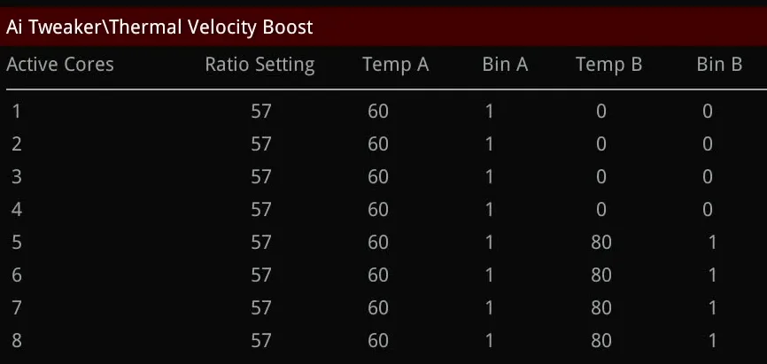
- Set 1- to 8-Core Active to Enabled
- For 1- to 8-Core Active, set Temperature A to 60
- For 1- to 8-Core Active, set Negative Ratio Offset to 1
- For 5- to 8-Core Active, set Temperature B to 80
- For 5- to 8-Core Active, set Negative Ratio Offset to 1
- Leave the Thermal Velocity Boost submenu
- Enter the Max Voltage Limits submenu
- Set P-Core Max Voltage Limits to 1.45
- Set E-Core Max Voltage Limits to 1.30
- Set Ring Max Voltage Limits to 1.30
- Leave the Max Voltage Limits submenu
- Enter the Performance Core V/F Point Offset submenu
- Set V/F Point Present Mode to All Core Mode
- Set V/F Point Voltage Control Mode to Manual Mode
- Set V/F Point 6 Offset to -35
- Set VF Point 7 Offset to -75
- Leave the Performance Core V/F Point Offset submenu
- Enter the Efficient Core V/F Point Offset submenu
- Set V/F Point Present Mode to All Core Mode
- Set V/F Point Voltage Control Mode to Manual Mode
- Set V/F Point 6 Offset to -50
- Leave the Efficient Core V/F Point Offset submenu
- Enter the Tweaker’s Paradise submenu
- Set High d2d cold boot workaround to Enabled
- Leave the Tweaker’s Paradise submenu
- Set Max. CPU Cache Ratio to 40
- Set NGU Ratio to 34
- Set CPU D2D Ratio to 36
- Set Actual VRM Core Input Voltage to Manual Mode
- Set CPU Core Voltage Override to 1.500
- Set Performance Core DLVR Voltage to Adaptive Mode
- Set Additional Turbo mode Voltage to 1.400
- Set Efficient Core DLVR Voltage to Adaptive Mode
- Set Additional Turbo mode Voltage to 1.250
- Set Ring DLVR Voltage to Adaptive Mode
- Set Additional Turbo mode Voltage to 1.200
- Set CPU System Agent Voltage to Manual Mode
- Set CPU System Agent Voltage Override to 1.300
- Set VNNAON 0.77v Voltage to Manual Mode
- Set VNNAON Voltage Override to 1.000
Then save and exit the BIOS.
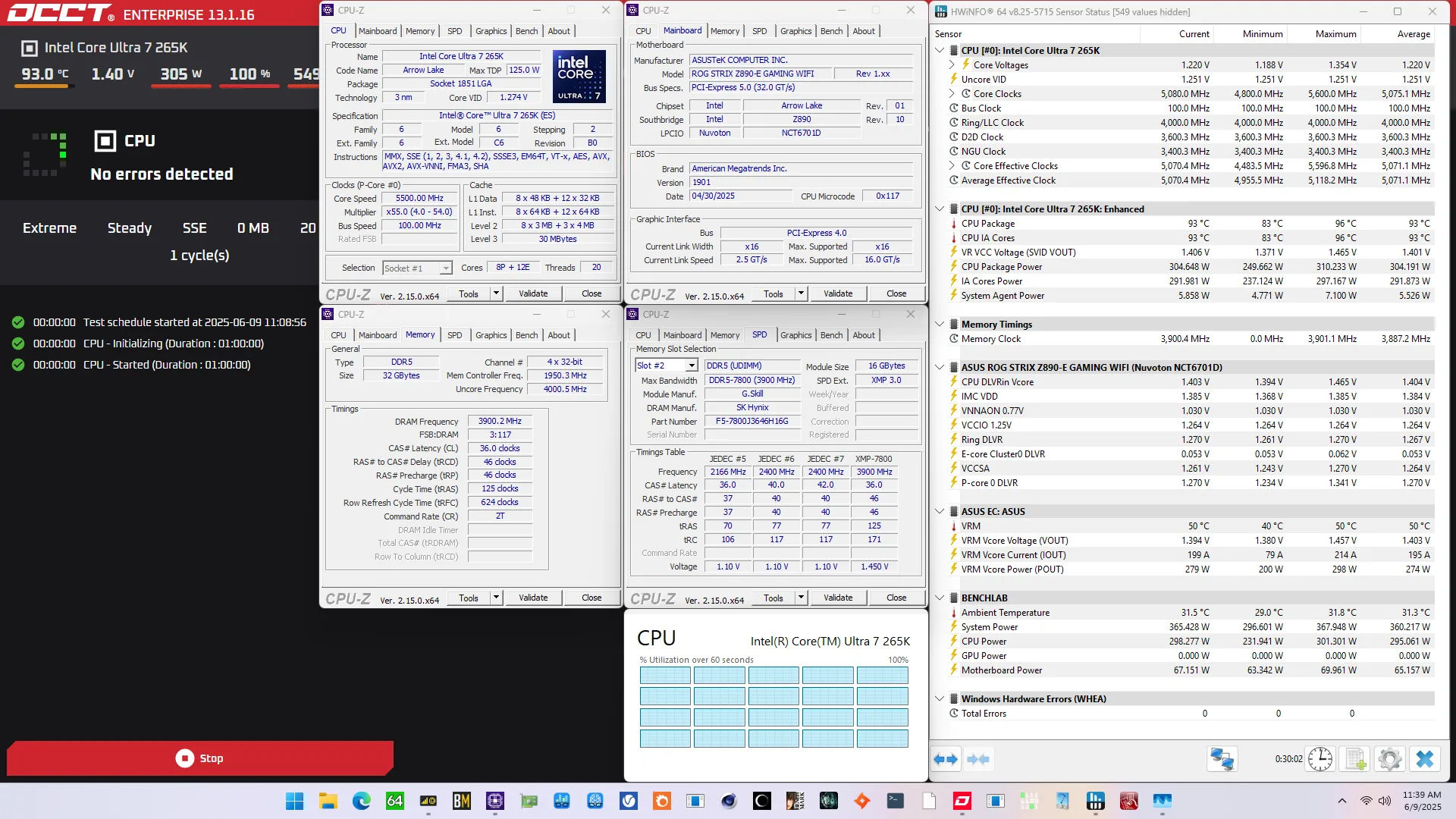
The CPU boost frequency with 1 active P-core is 5700 MHZ and remains so even when all P-cores are active. Then, it gradually reduces to 5160 MHz when all P- and E-cores are active. In single-threaded applications, all P-cores can boost to 5700 MHz and every E-core can boost to 4.9 GHz.
We re-ran the benchmarks and checked the performance increase compared to the default operation.
Our finetuning efforts primarily impact low intensity workloads as the frequency is decreased at 60 and 80 degrees Celsius. So, we’re not expecting great performance improvements. That’s exactly what we see. The Geomean performance improves by another percentage point, and we get a maximum improvement of +31.33% in PyPrime.

When running the OCCT CPU AVX2 Stability Test, the average CPU P-core effective clock is 5500 MHz with 1.267 volts and the average CPU E-core effective clock is 4801 MHz with 1.189 volts. The average CPU temperature is 98.0 degrees Celsius. The average CPU package power is 326.6 watts.
When running the OCCT CPU SSE Stability Test, the average CPU P-core effective clock is 5495 MHz with 1.268 volts and the average CPU E-core effective clock is 4787 MHz with 1.251 volts. The average CPU temperature is 93.0 degrees Celsius. The average CPU package power is 304.2 watts.
OC Strategy #5: DRAM Tuned
In our final overclocking strategy, we try to tune the memory sub system and adjust the DRAM timings to see if it has any impact on system performance. For this I rely on the ASUS Memory Presets and manual timing adjustments.
Memory Presets
ASUS Memory Presets is an ASUS overclocking technology that provides you with a selection of memory tuning presets for certain memory ICs. The presets will adjust the memory timings and voltages.
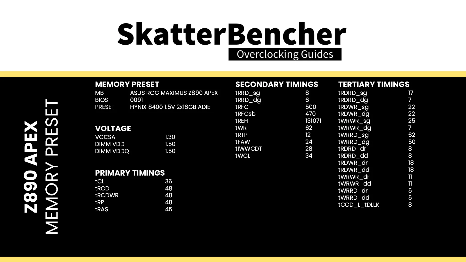
Not all boards have Memory Presets available – for example, this ROG Strix Z890-E Gaming. Luckily, I had a Z890 Apex on hand and could copy over the timings from the Hynix 8400 1.5 2x16GB ADIE profile. For your reference, you can find the relevant timings below.
DRAM Tuning
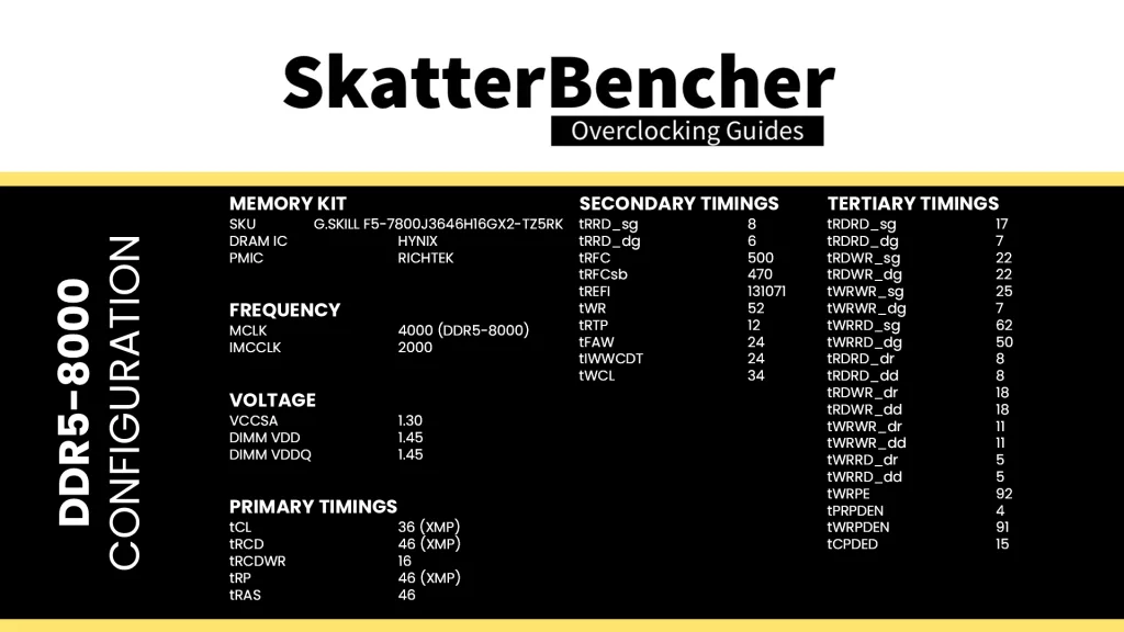
It’s of course not a given that copying over timings will work with any 2x16GB Hynix kit. Fortunately, I had already tuned this kit when I overclocked the Core Ultra 5 245K in SkatterBencher #83.
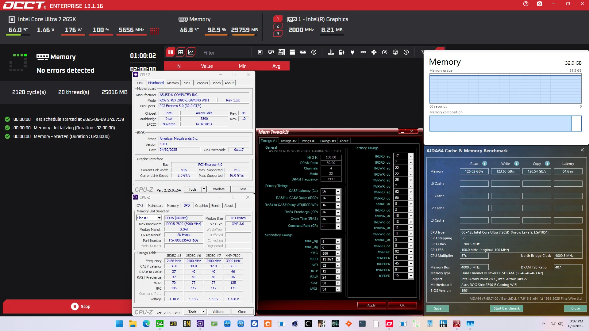
Here is my final memory configuration:
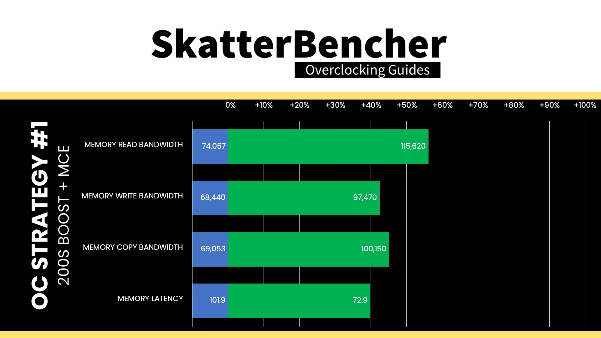
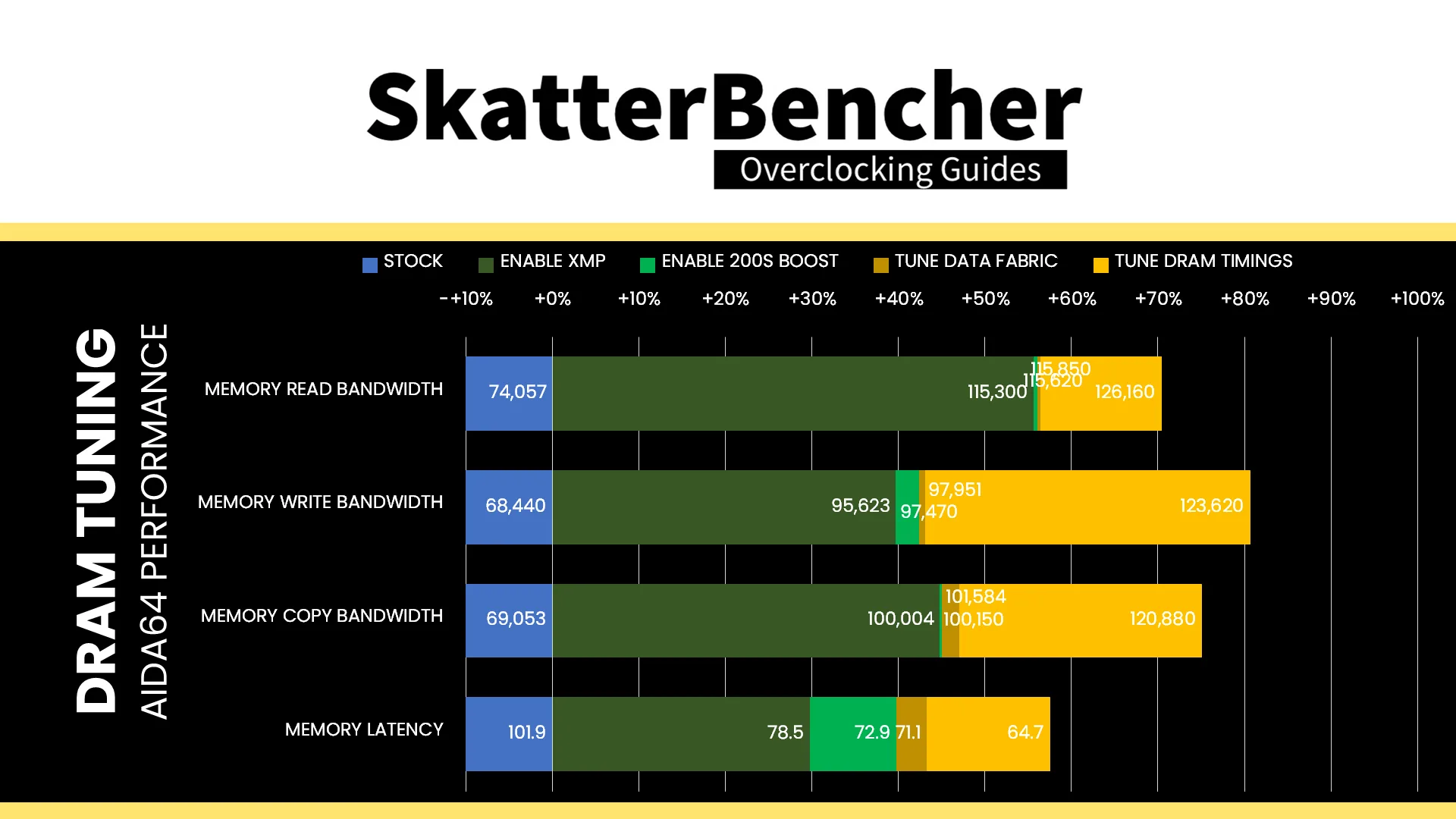
After the tuning, our AIDA64 performance improved quite significantly. We got about +50% extra bandwidth and +30% better latency enabling XMP. Enabling 200S Boost added a couple more percentage of bandwidth and improved the latency by 10%. Further tuning the fabric added a couple of percentage points. Then, tuning the memory added another 14 to 38% extra bandwidth and further improved the latency by 14%.
BIOS Settings & Benchmark Results
Upon entering the BIOS
- Go to the Ai Tweaker menu
- Set Performance Preferences to ASUS Advanced OC Profile
- Set Ai Overclock Tuner to XMP I
- Set ASUS MultiCore Enhancement to Enabled – Remove All Limits
- Set Performance Core Ratio to By Core Usage
- Set 1-Core to 8-Core Ratio Limit to 57
- Set Efficient Core Ratio to By Core Usage
- Enter the By E-Core Usage submenu
- Set Efficient Turbo Ratio Limit 1 to 49
- Set Efficient Turbo Ratio Cores 1 to 6
- Set Efficient Turbo Ratio Limit 2 to 48
- Set Efficient Turbo Ratio Cores 2 to 12
- Leave the By E-Core Usage submenu
- Set DRAM Frequency to DDR5-8000
- Enter the DRAM Timing Control submenu
- Set DRAM timings accordingly
- Leave the DRAM Timing Control submenu
- Enter the DIGI+ VRM submenu
- Set CPU Load-line Calibration to Level 6
- Leave the DIGI+ VRM submenu
- Enter the Thermal Velocity Boost submenu
- Set TVB Voltage Optimizations to Disabled
- Set Enhanced TVB to Disabled
- Set Overclocking TVB to Enabled
- Set OC TVB Configuration Limit to Per P-core Group
- Set OC TVB Ratio Item Mode to Per Core Mode
- Set 1- to 8-Core Active to Enabled
- For 1- to 8-Core Active, set Temperature A to 60
- For 1- to 8-Core Active, set Negative Ratio Offset to 1
- For 5- to 8-Core Active, set Temperature B to 80
- For 5- to 8-Core Active, set Negative Ratio Offset to 1
- Leave the Thermal Velocity Boost submenu
- Enter the Max Voltage Limits submenu
- Set P-Core Max Voltage Limits to 1.45
- Set E-Core Max Voltage Limits to 1.30
- Set Ring Max Voltage Limits to 1.30
- Leave the Max Voltage Limits submenu
- Enter the Performance Core V/F Point Offset submenu
- Set V/F Point Present Mode to All Core Mode
- Set V/F Point Voltage Control Mode to Manual Mode
- Set V/F Point 6 Offset to -35
- Set VF Point 7 Offset to -75
- Leave the Performance Core V/F Point Offset submenu
- Enter the Efficient Core V/F Point Offset submenu
- Set V/F Point Present Mode to All Core Mode
- Set V/F Point Voltage Control Mode to Manual Mode
- Set V/F Point 6 Offset to -50
- Leave the Efficient Core V/F Point Offset submenu
- Enter the Tweaker’s Paradise submenu
- Set High d2d cold boot workaround to Enabled
- Leave the Tweaker’s Paradise submenu
- Set Max. CPU Cache Ratio to 40
- Set NGU Ratio to 34
- Set CPU D2D Ratio to 36
- Set Actual VRM Core Input Voltage to Manual Mode
- Set CPU Core Voltage Override to 1.500
- Set Performance Core DLVR Voltage to Adaptive Mode
- Set Additional Turbo mode Voltage to 1.400
- Set Efficient Core DLVR Voltage to Adaptive Mode
- Set Additional Turbo mode Voltage to 1.250
- Set Ring DLVR Voltage to Adaptive Mode
- Set Additional Turbo mode Voltage to 1.200
- Set CPU System Agent Voltage to Manual Mode
- Set CPU System Agent Voltage Override to 1.300
- Set VNNAON 0.77v Voltage to Manual Mode
- Set VNNAON Voltage Override to 1.000
Then save and exit the BIOS.
We re-ran the benchmarks and checked the performance increase compared to the default operation.
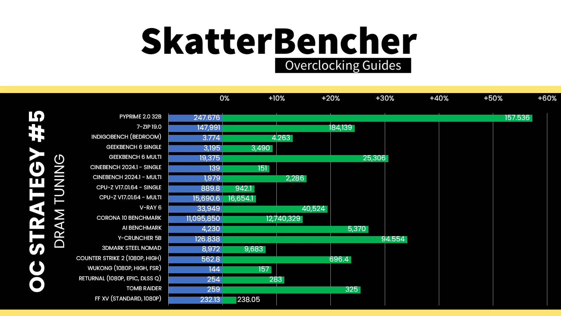
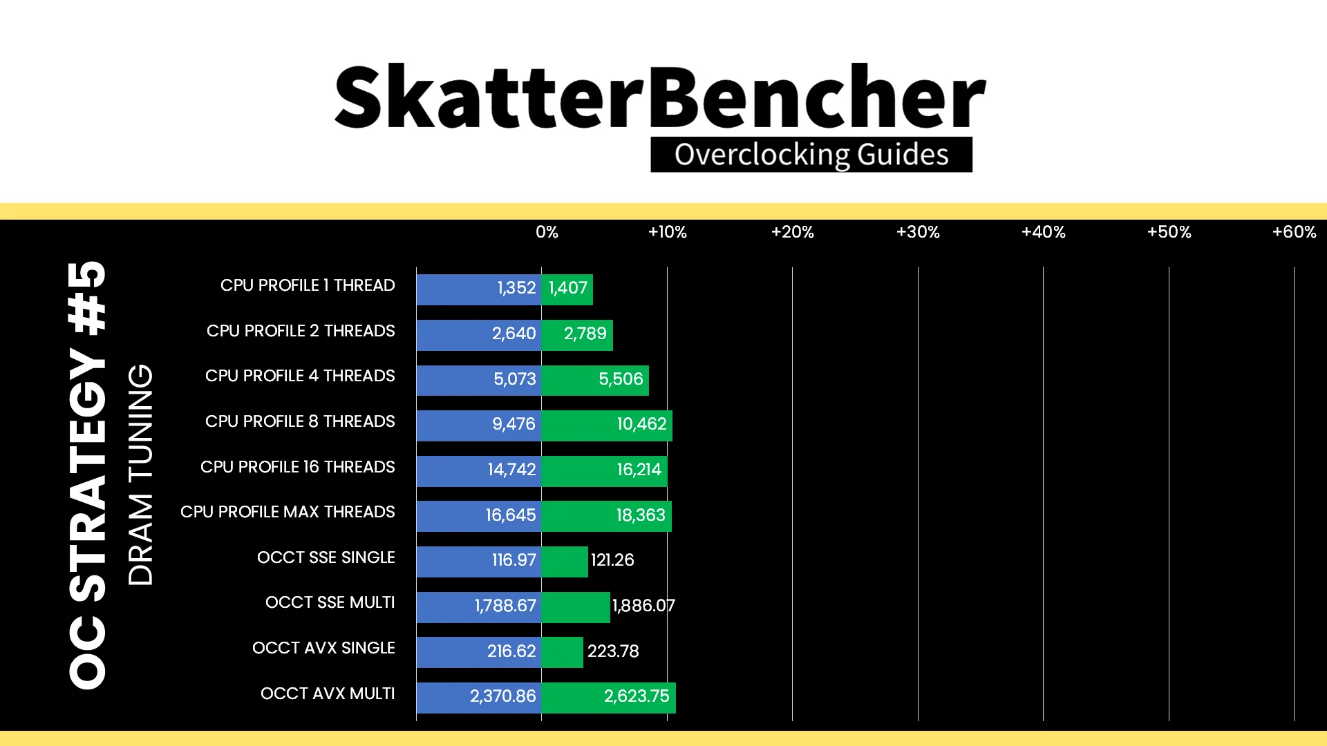
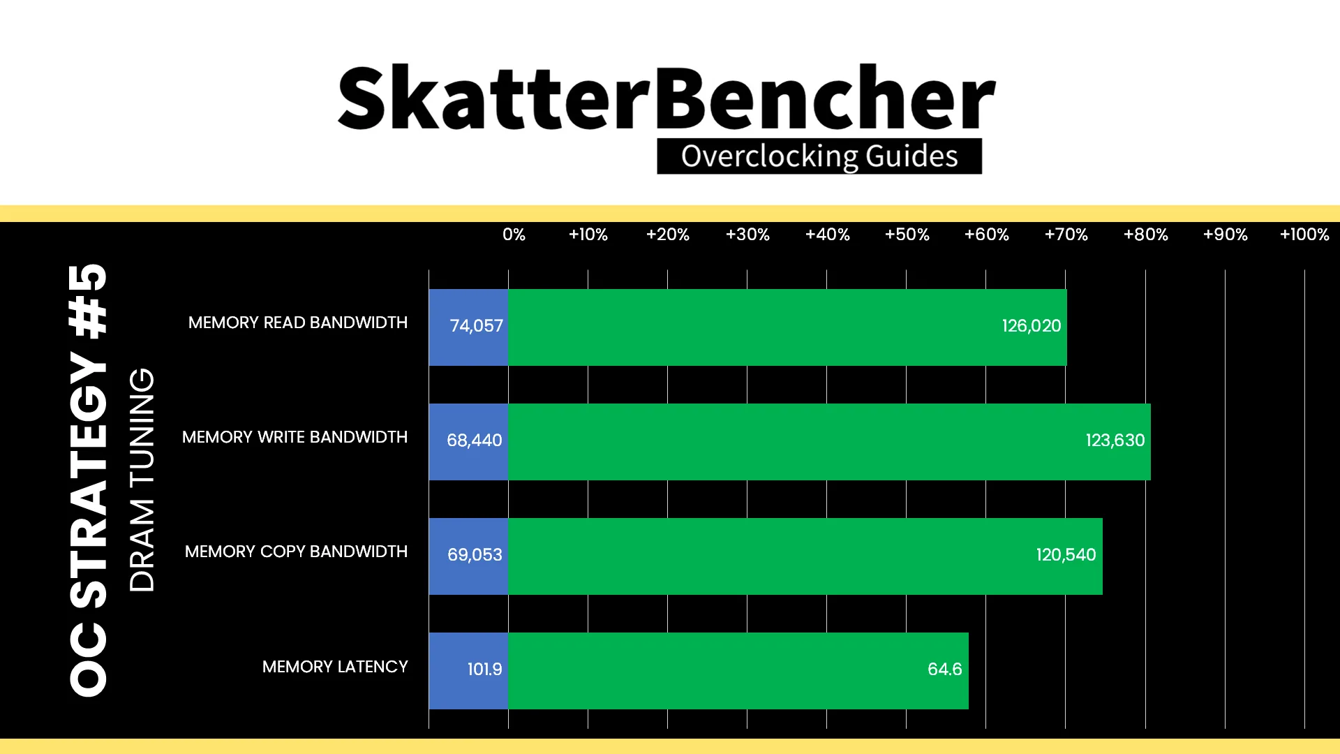
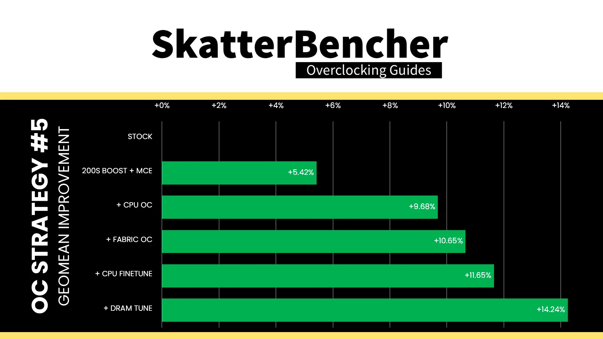
Tuning the memory timings and adding a little bit of frequency doesn’t have the enormous impact some would expect. However, it’s nonetheless interesting to still see performance improve, especially in multi-threaded workloads like AI Benchmark and Y-Cruncher. The Geomean performance improves by almost three percentage points, and we get a maximum improvement of +57.22% in PyPrime.
Intel Core Ultra 7 265K: Conclusion
Let’s wrap this up.
The Core Ultra 7 265K is the final of the three Arrow Lake K-SKU processors I wanted to make a SkatterBencher guide for. The overclocking experience is similar to that of the 285K and 245K: minimal headroom for the P-cores, nice boost from the E-cores, and everything seems to add performance.
That last part is what makes tuning Arrow Lake so interesting to me: it really seems that everything you do – whether that’s pushing the cores, fabric, or tuning the memory timings – results in additional performance.
Anyway, that’s it for my Arrow Lake overclocking adventures. I want to thank my Patreon supporters and YouTube members for supporting my work. If you have any questions or comments, please drop them in the comment section below.
See you next time!