Arrow Lake Graphics Overclocking

We have a closer look at tuning the performance of the the Arrow Lake Graphics, located on the Graphics Tile.
Arrow Lake is Intel’s revolutionary new processor for mainstream desktop, featuring new P-cores and E-cores, disaggregated tile-based 3D Foveros packaging, an integrated NPU for AI acceleration, a next-generation uncore, DLVR power rails, and so much more.

In this blog post series, I have a closer look at Arrow Lake and explore its performance tuning and overclocking opportunities. I will cover the Compute (P-core, E-core, Graphics, NPU), Memory Subsystem (DDR, MC), and Data Fabric (Ring, NGU, D2D).
Arrow Lake Graphics: Introduction
The Arrow Lake integrated graphics are located on the Graphics Tile and thus disconnected from the other Compute IP blocks. The graphics tile is manufactured using the TSMC N3 process. It doesn’t share the tile with any other IP blocks. Not even the media engine.
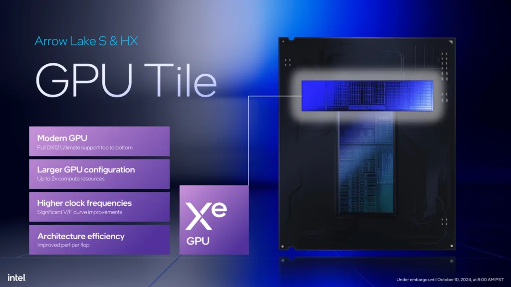
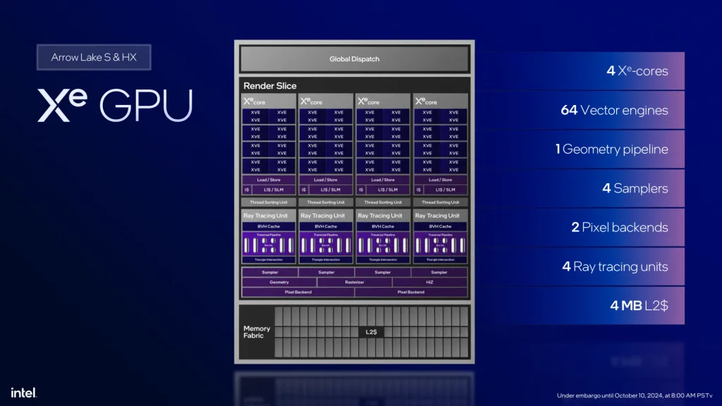
The integrated graphics features 4 Xe-LPG cores. This is an improved version of the Xe-LP cores from Raptor Lake which effectively doubles the Execution Units. However, it still features the Alchemist architecture. The 4 Xe-cores consist of 64 execution units and 512 shader units.
Arrow Lake Graphics: Clocking
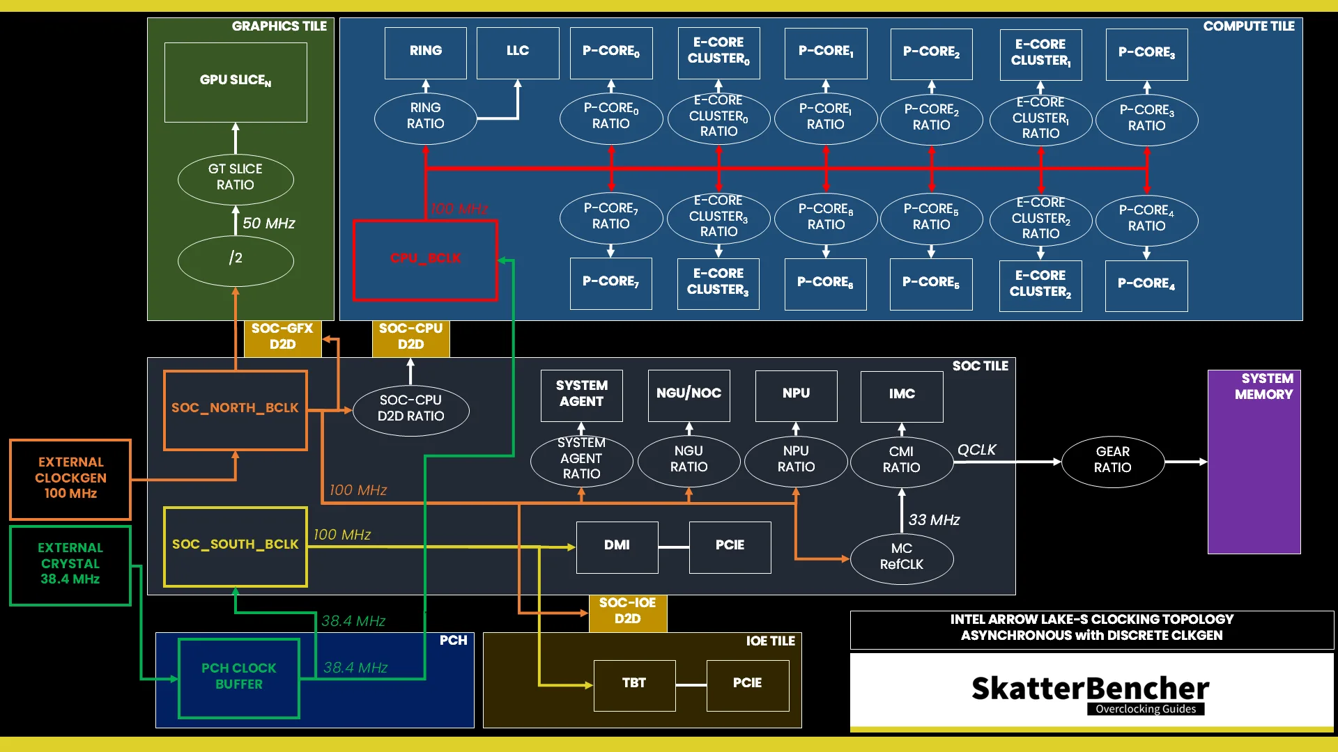
The clocking of the integrated graphics (GT) is similar to previous architectures: a reference clock is multiplied with a ratio to achieve the eventual operating frequency.
Reference Clock
The 100MHz reference clock is generated internally by the SoC PLL. However, it can also be clocked with an external clock generator providing the reference clock for the SoC PLL. This clock affects nearly all the IP blocks of Arrow Lake, except for those in the Compute Tile and the PCIe/DMI links. This PLL can be linked to the CPU PLL when you run in synchronous mode or work independently if you run asynchronous mode.
You can configure the SOC BCLK frequency between 40 and 1000 MHz. The 100 MHz reference clock is divided by two (2) to achieve a 50 MHz base clock frequency.
In the ASUS ROG BIOS, you can configure the SOC BCLK Frequency in the Ai Tweaker menu by first setting the Ai Overclock Tuner option to anything else than Auto.
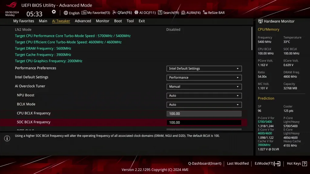
You can switch between Asynchronous and Synchronous mode by adjusting the BCLK mode option.

Graphics Ratio
The reference clock is multiplied by the GT Slice ratio to achieve the final clock frequency. The GT Ratio is determined by the Graphics Dynamic Frequency technology.
Graphics Dynamic Frequency
The Graphics Dynamic Frequency capability is designed to allow the processor to assess its thermals, current, and power to come up with a dynamic upper limit on its graphics frequency. On processors with Graphics Overclocking capability, the integrated graphics cores can run at frequencies higher when operating conditions allow.
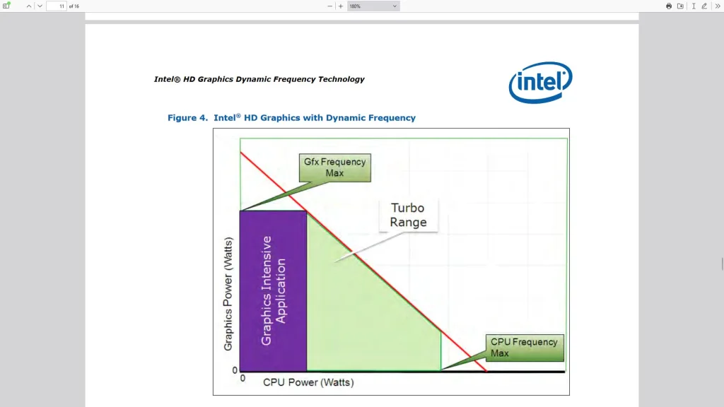
When Graphics Dynamic Frequency is enabled, the graphics cores could be running at any ratio in the inclusive range between the Maximum Dynamic Frequency (RP0) and the Graphics Base Frequency (RP1). In the case of our Core Ultra 9 285K, the graphics base frequency is 300 MHz, and the default maximum dynamic frequency is 2000 MHz. When overclocking, we simply increase this Maximum Dynamic Frequency (RP0) to a higher value.
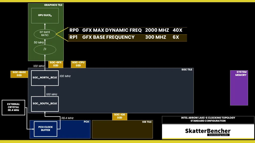
The GT Ratio starts from 1X. The default ratio is 40X, which yields a 2 GHz operating frequency. The maximum configurable ratio is 85X.
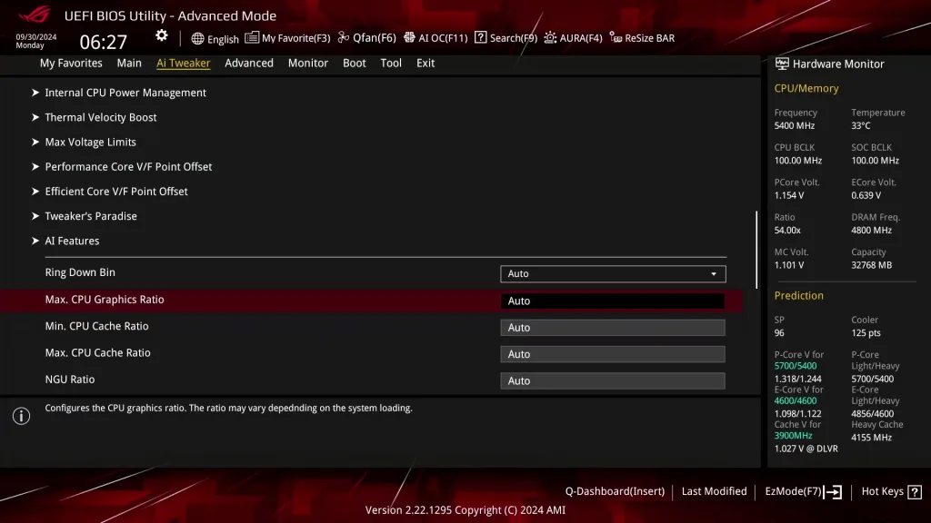
In the ASUS ROG BIOS, you can configure the Graphics Maximum Dynamic Frequency via the Ai Tweaker menu.
Arrow Lake Graphics: Voltage
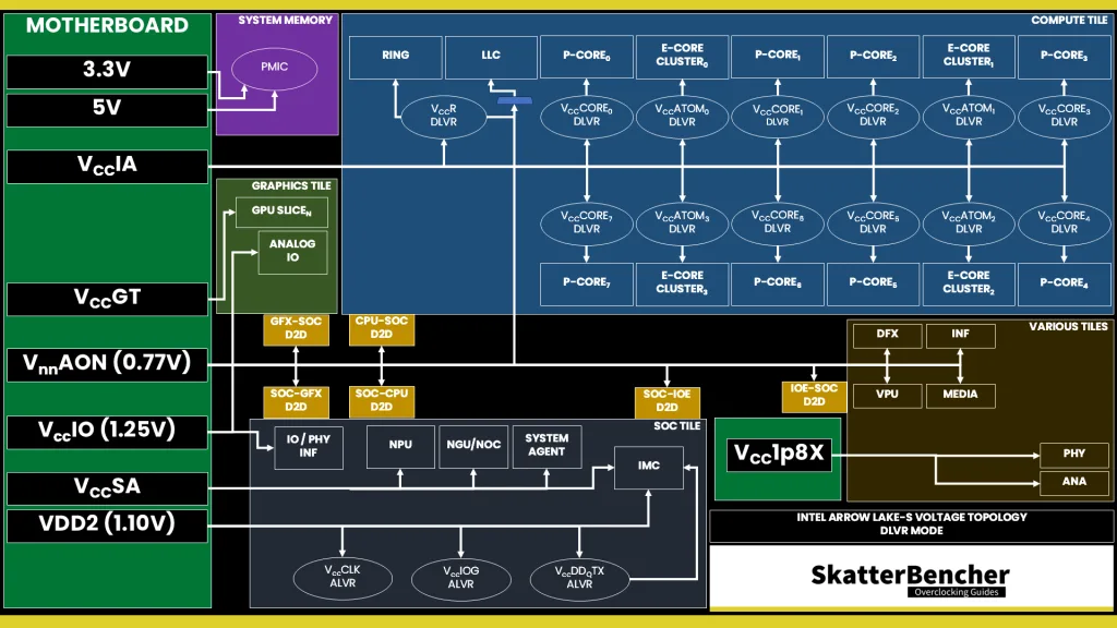
The voltage regulation for the integrated graphics is nearly the same as on prior Intel Core processors.
V/F Curve
The integrated graphics relies on a V/F curve defined by up to seven (7) V/F points. The first six (6) V/F points are factory-fused and the last point is mapped to the “OC Ratio.”

Here is the GT V/F curve for my specific Core Ultra 9 285K. The voltage is about 700 mV at 400 MHz, then increases to 984 mV for VF Point 6 at 2 GHz.
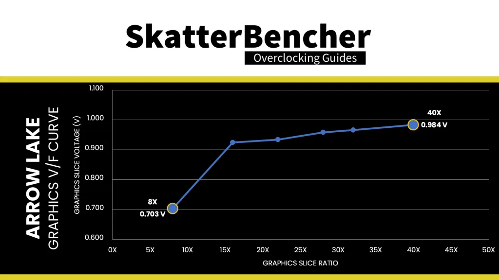
2.0 GHz is the default maximum frequency for the integrated graphics. Unfortunately, the graphics V/F Points are not available in the ASUS ROG BIOS.
Voltage Limits
To safeguard the processor, Intel has imposed strict voltage limits for several IP blocks, including the integrated graphics. This limit effectively prevents the GT from requesting higher voltage to the VccGT voltage controller.
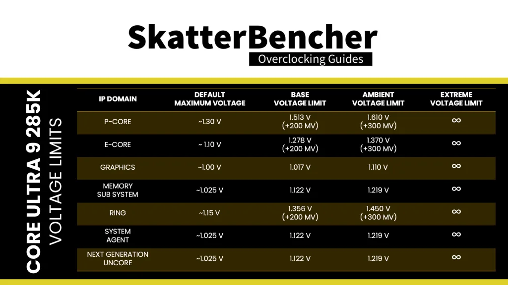
By default, the voltage limit for the GT is 1.017V, but this can be increased to 1.110V under ambient conditions. When the temperature is below 10 degrees Celsius, you can further increase the voltage limit or disable the limit altogether.
Of course, in Power Gate PMBus mode you can override the voltage limit and set any voltage you want. Of course, motherboard vendors can implement their own voltage limits for the voltage regulator.
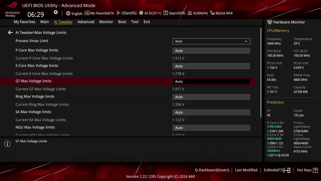
In the ASUS ROG BIOS, you can configure the integrated graphics Voltage Limit via the Ai Tweaker Max Voltage Limits sub-menu.
VccGT MBVR
The external VccGT MBVR provides the voltage rail for integrated graphics. Unlike the other compute IP blocks, it does not have a DLVR to manage the voltage. So, the power delivery is identical to the previous architecture. We can refer to it as Power Gate (PG) mode.
VccGT Power Gate SVID Mode
Based on its VF curve, the integrated graphics request an operating voltage using the SVID protocol from the CPU Power Control Unit (PCU). The PCU in turn configures the VccGT voltage rail.
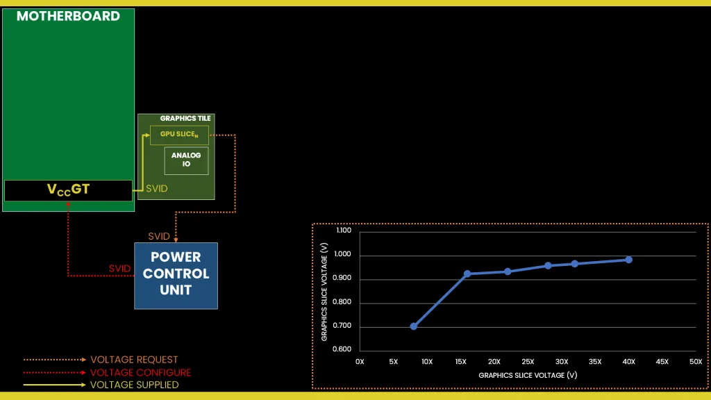
There are two ways to configure the graphics voltage:
- Adaptive mode is the standard mode of operation, which relies on the factory-fused voltage-frequency curves we discussed before.
- Override mode specifies a single static voltage across all ratios. It is mainly used for extreme overclocking where stability at high frequencies is the only consideration.
We can configure override and adaptive modes directly in the PCU by specifying a target voltage and a voltage offset for each mode. In adaptive mode, the target voltage is mapped to the GT’s “OC Ratio.” This also matches VF Point 7. You can configure the adaptive voltage and OC Ratio to any value, however, multiple rules enforce what ratio and voltage are actually set.
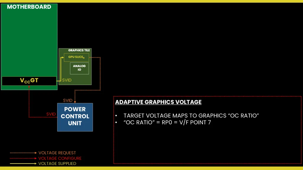
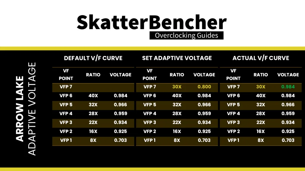
Rule #1: the voltage set for a given VF Point n must be higher than or equal to the voltage set for VF Point n-1.
In the case of the GT, it means that the voltage for the OC Ratio must be higher than or equal to the voltage for VF Point 6. This can be a little strange because you can program the OC ratio to any value, including lower than 40X.
For example, let’s say you set the GT ratio to 30X and the adaptive voltage to 0.8V. In that case, VF Point 7 will be programmed to 30X at 0.8V. However, the actual frequency will be 1.5 GHz with 0.984, as that’s the voltage for VF Point 6.
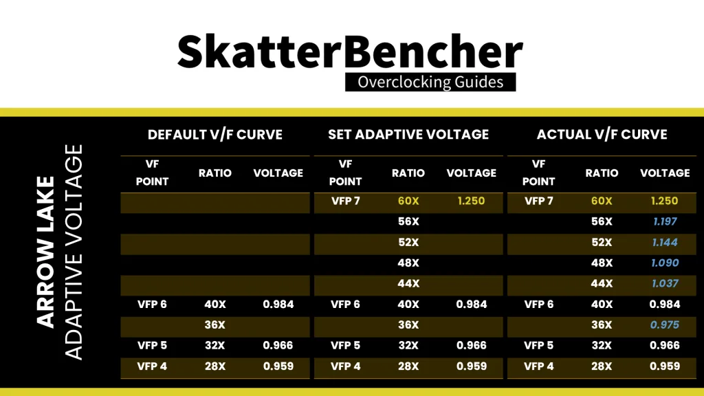
Rule #2: for ratios between the OC Ratio and the next highest factory-fused V/f point, the voltage is interpolated between the set adaptive voltage and the factory-fused voltage.
Let’s say we configure the GT OC Point to 60X and 1.25V. The target voltage for GT ratios between 40X and 60X is now interpolated between the factory-fused voltage for 40X and the set adaptive voltage for 60X.
One last thing about the adaptive mode. The adaptive offset is applied across the entire curve. So, if we set +100 mV adaptive offset, the operating voltage for all frequencies between 8X and the OC ratio will be increased by 100 mV.
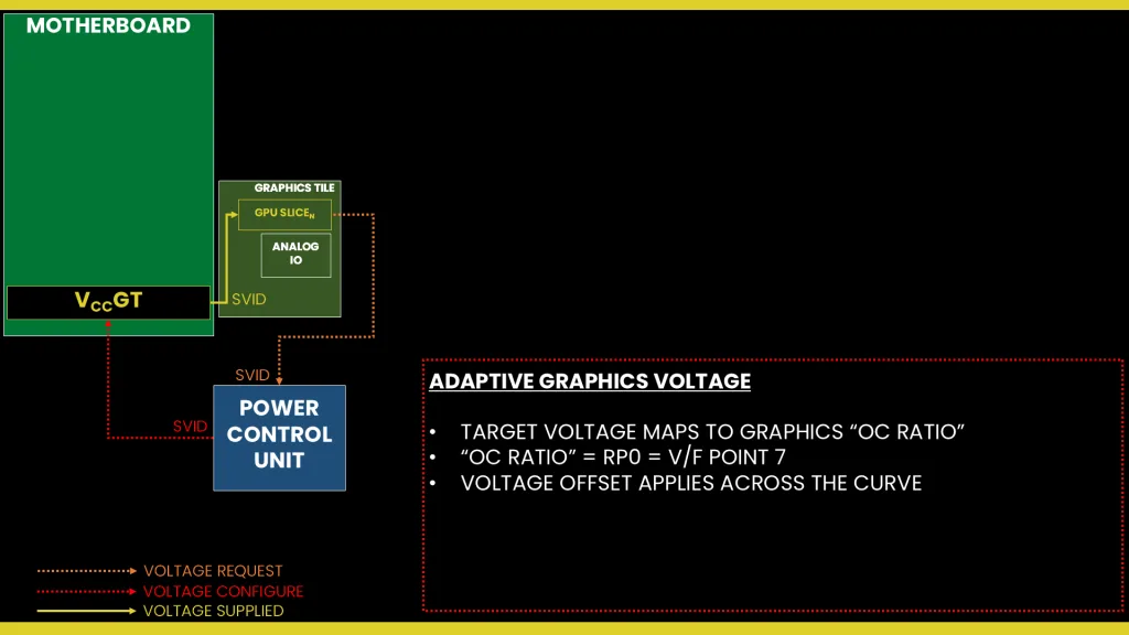
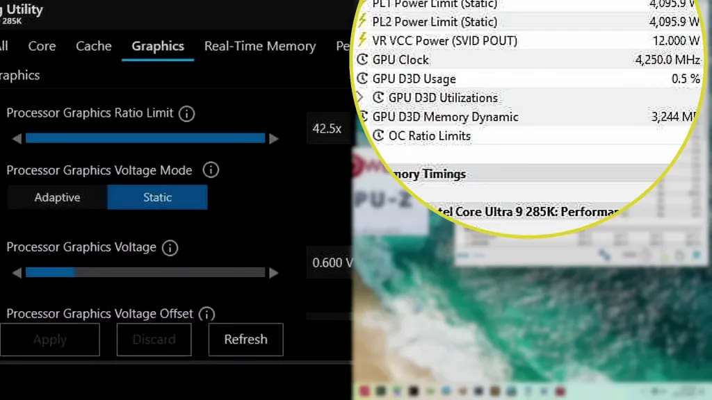
Unfortunately, the graphics adaptive voltage SVID configuration is not available in the ASUS ROG BIOS. However, you can access it using Shamino’s work tool or configure it using Intel Extreme Tuning Utility.
VccGT Power Gate PMBus Mode
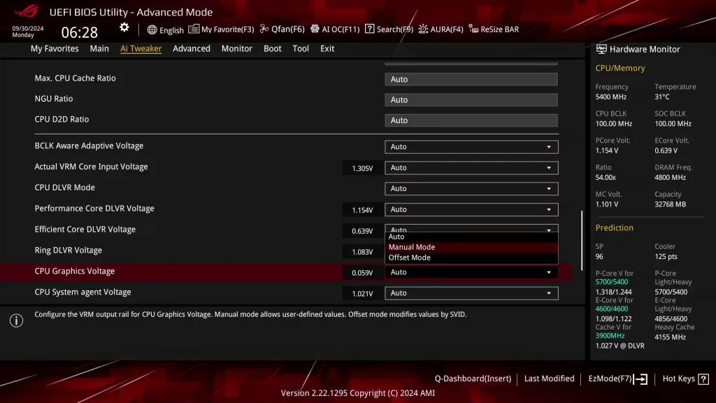
As mentioned, the GT adaptive voltage SVID mode is not available in the ASUS BIOS. However, that doesn’t mean we can’t configure the graphics voltage as there’s a second way to approach Power Gate Mode voltage configuration: ignore the SVID voltage requests and calculations, and program the VccGT voltage regulator directly over PMBus. This process effectively allows us to take full control over the voltage set by the VccGT voltage rail.
This approach is a very traditional way of overclocking whereby you set a fixed output voltage and then use an appropriate VRM loadline setting – if available – to reduce the operating voltage in higher load scenarios. The loadline configuration isn’t particularly useful for integrated graphics.
In the case of the integrated graphics, using Power Gate PMBus mode appears to offer better overclocking headroom because the PCU uses the SVID requests to estimate some power metrics. If the SVID is too high, the GT is throttled and performance is capped.
In the ASUS ROG BIOS, you can set the VccGT voltage rail in the Ai Tweaker menu by configuring the CPU Graphics Voltage in manual mode.
Arrow Lake Graphics: Power
The processor power consumption is primarily governed by the Turbo Boost 2.0 Technology.
Turbo Boost 2.0 Technology
Intel Turbo Boost 2.0 Technology allows the processor cores and graphics to run faster than the base operating frequency if the processor is operating below rated power, temperature, and current specification limits. The ultimate advantage is opportunistic performance improvements in CPU and graphics workloads.
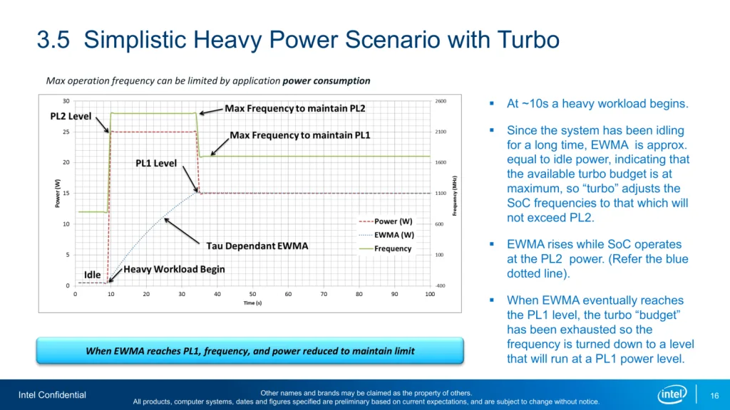
The turbo boost algorithm works according to an EWMA formula. This stands for Exponentially Weighted Moving Average. There are three main parameters to consider: PL1, PL2, and Tau.
- Power Limit 1, or PL1, is the threshold that the average power will not exceed. Historically, this has always been set equal to Intel’s advertised TDP. Very importantly, PL1 should not be set higher than the thermal solution cooling limits.
- Power Limit 2, or PL2, is the maximum power the processor is allowed to use for a limited amount of time.
- Tau is a weighing constant used in the algorithm to calculate the moving average power consumption. Tau, in seconds, is the time window for calculating the average power consumption. If the average power consumed is higher than PL1 the CPU will reduce the CPU frequency.
Turbo Boost 2.0 Technology has evolved over the past years to incorporate many power, thermal, and electrical performance limiters, including PL3, PL4, IccMax, TCC_Offset, VR_TDC, RATL, Pmax, and many more. To cover each in this blog post would take up too much time.
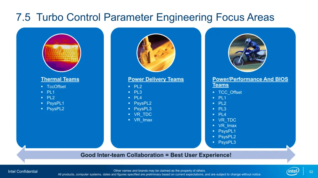
Note that while the CPU cores and graphics power management both fall under the purvey of the Turbo Boost 2.0 technology, each component also has individual limits. For example, the graphics performance may be throttled due to a VccGT voltage rail-specific limiter like VR_TDC even though there’s plenty of overall Turbo Boost budget available.
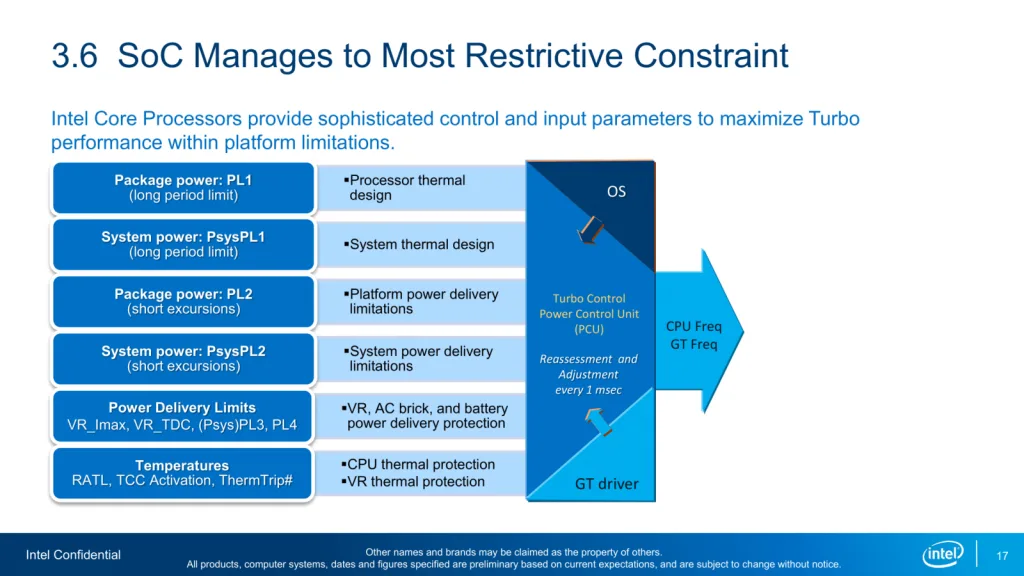
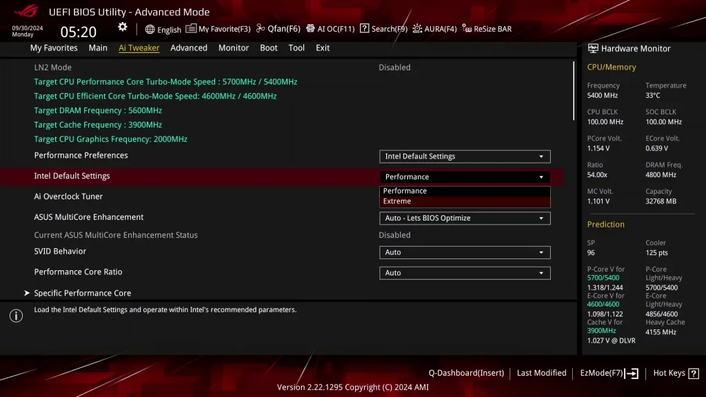
Intel provides two performance profiles for the Arrow Lake SKUs which configure all these settings for you. For the Core Ultra 9 285K, the Turbo Boost 2.0 profiles are Performance and Extreme.
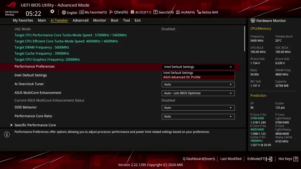
In the ASUS ROG BIOS, you can switch between Intel Default Performance Profiles in the Ai Tweaker menu by setting the Performance Preference menu item to Intel Default Settings and selecting one of the two Intel Default Settings options.
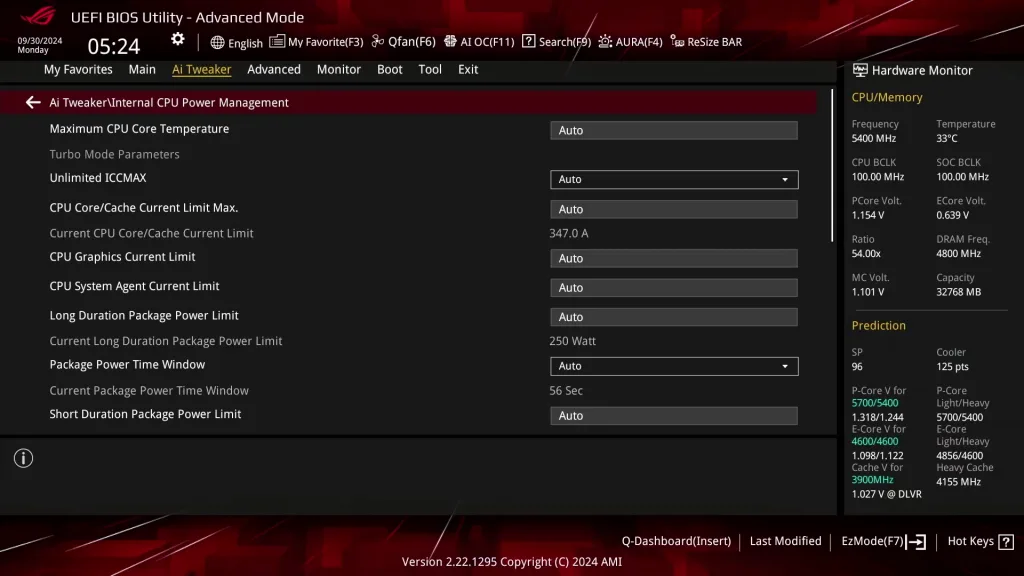
Should you wish to override the performance profiles, you can do so in two ways: either by manually configuring them in the BIOS or by enabling ASUS Multi-Core Enhancement.
In the ASUS ROG BIOS, you can find many Turbo Boost 2.0 parameter options in the Ai Tweaker Internal CPU Power Management sub-menu.
ASUS MultiCore Enhancement
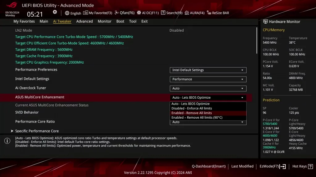
ASUS MultiCore Enhancement enables higher out-of-the-box performance for heavy, power-hungry, multi-threaded workloads. It does this by optimizing the Turbo Boost 2.0 configuration. There are four available options.
- Auto, let the ASUS motherboard decide.
- Disabled – Enforce All Limits, following the Intel guidelines for Turbo Boost 2.0 power and ratio configuration
- Enabled – Remove All Limits, unleashes the Intel Turbo Boost 2.0 power limits for maximum performance.
- Enabled – Remove All Limits (90C), unleashes the Intel Turbo Boost 2.0 power limit but restricts the maximum CPU temperature to 90 degrees Celsius.
Note that you can select an Intel Performance Profile and enable MCE at the same time. The effect will be that MCE overrides the most common Turbo Boost 2.0 parameters such as PL1 and PL2, but will adhere to other limiters such as Current Excursion Protection (CEP) configured by the Intel Performance Preset.
In the ASUS ROG BIOS, you enable ASUS MCE in the Ai Tweaker menu.
ASUS Advanced OC Profile
The ASUS Advanced OC Profile is a more elaborate unleashed overclocking profile than MultiCore Enhancement as it not only adjusts the major Turbo Boost 2.0 parameters but also implements a lot of BIOS auto-rules to facilitate overclocking.
In the ASUS ROG BIOS, you can switch to the ASUS Advanced OC Profile in the Ai Tweaker menu by setting the Performance Preference menu item.
Arrow Lake Graphics: Overclock & Undervolt
Overclocking the integrated graphics is similar to how it was on Raptor Lake.
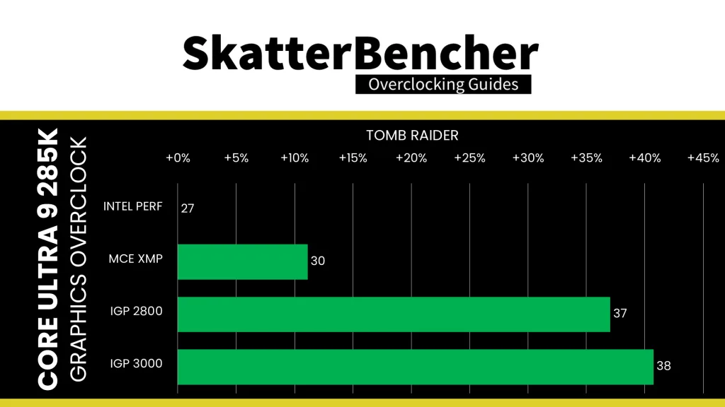
At the default frequency of 2 GHz with DDR5-4800 memory, we get about 27 FPS in Tomb Raider. When enabling MCE and pairing the IGP with DDR5-8000 memory, that increases to 30FPS. However, the biggest performance increase comes from overclocking the graphics frequency.
We can quite easily increase the frequency to 2.8 GHz by using the 56X ratio. That increases the Tomb Raider performance to 37 FPS. Then, things get a little more tricky because we’re starting to trigger some power limits.
To make a long story short: the CPU calculates an expected power consumption based on the voltage requested by the IGP to the VccGT voltage controller. We know this problem very well from the Arc A380 and A780 discrete graphics cards I overclocked on this channel before.
The easy solution is to switch the voltage controller to PMBus mode. That simply cuts the communication line between the graphics and the VccGT voltage controller. Then, we can set the voltage controller to output any voltage while telling the integrated graphics to only request 600mV.
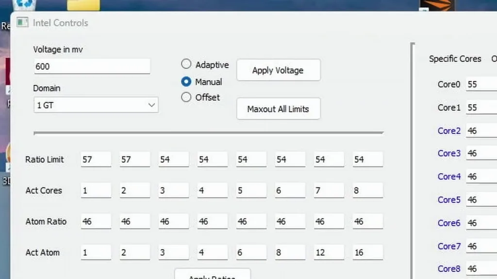
With this trick, we can further increase the IGP frequency to 3000 GHz with 1.35V.

That results in a Tomb Raider performance of 38 frames per second.

Arrow Lake Graphics: Extreme Overclock
The Arrow Lake Integrated Graphics are remarkably good at overclocking and scaling with temperature and voltage. In the video below, I show the overclocking performance with liquid nitrogen cooling.
Here are the maximum achieved overclocks:
- 3700 MHz Tomb Raider
- 3700 MHz 3DMark Solar Bay
- 3800 MHz Final Fantasy XV
- 3900 MHZ GPU-Z Render Test
- 4250 MHz Windows Desktop
