SkatterBencher #42: NVIDIA GeForce GTX 1650 Overclocked to 2205 MHz
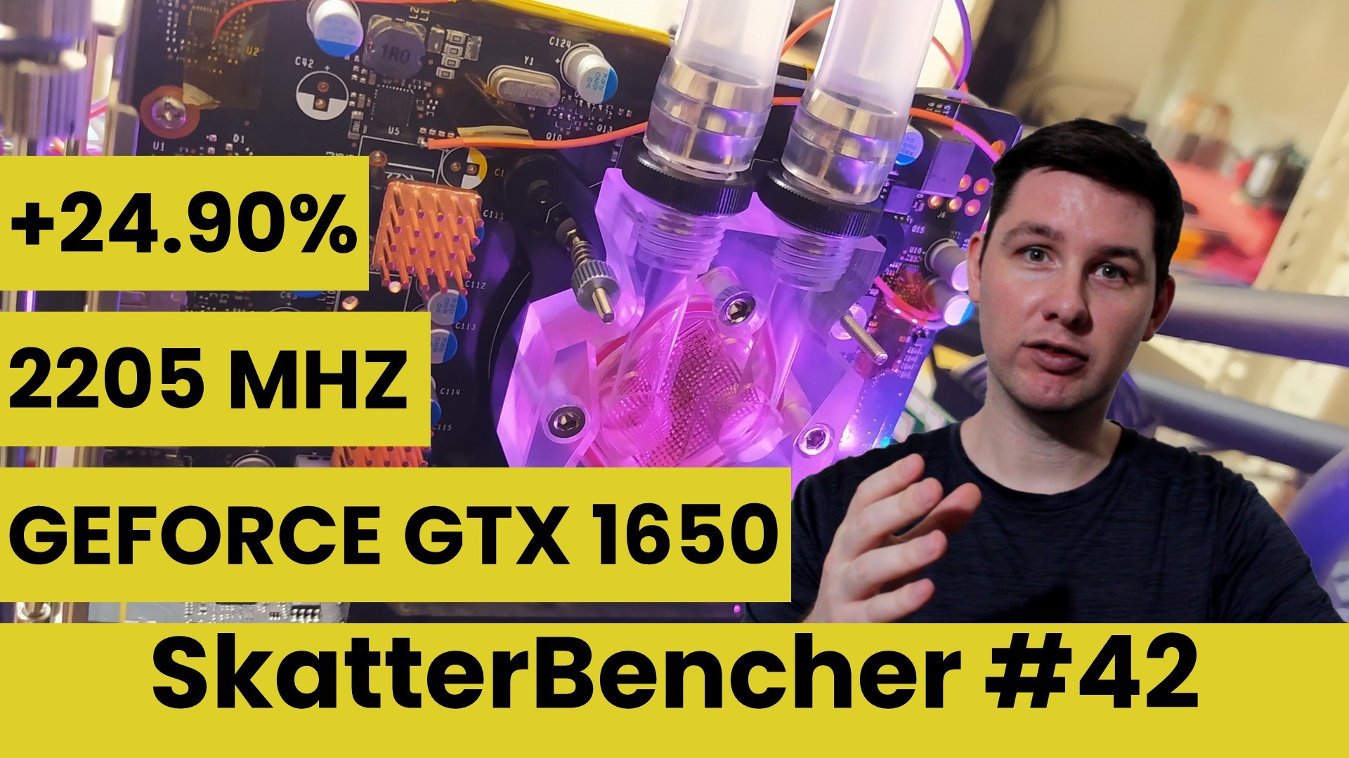
We overclock the NVIDIA GeForce GTX 1650 up to 2205 MHz with using the ElmorLabs EVC2SX and GPU water cooling.
This was my first look at an NVIDIA Turing graphics card, and naturally, I preferred to first have a go at the most low-end version, the TU117. The GT 1030 video from a couple of weeks ago helped my approach to overclock this card.
I hope you enjoy the video!
Table of Contents
NVIDIA GeForce GTX 1650: Introduction
The NVIDIA GeForce GTX 1650 is the slowest graphics card in NVIDIA’s Turing lineup. NVIDIA released the GTX 1650 on April 23, 2019, about one year and a half after the release of its bigger brother, the GTX 2080 TI.
The GeForce 16 series is unusual. Typically, all products of one GPU architecture are included in one product series. However, due to the lack of raytracing capabilities, the GTX Turing products are not included in the GeForce 20 series with the RTX Turing products.
About 1 year after the original GTX 1650, NVIDIA launched a GDDR6 version featuring the faster 12Gbps GDDR6 memory. In June 2020, NVIDIA announced a third version of the GTX1650 featuring the TU106 die borrowed from RTX 20-series graphics cards like the RTX 2070. While the TU106 die comes with NVIDIA Tensor and RT cores, these parts of the GPU are fused off when used for a GTX 1650 graphics card. Our card uses the original TU117 die and GDDR6 memory.
The GeForce GTX 1650 with GDDR6 is built on the TSMC 12nm process and houses 896 CUDA cores. It comes with a base clock of 1410 MHz and a boost clock of 1590 MHz. The 4GB GDDR6 variant has the memory clock in at 1500 MHz. The graphics card power is limited to 75W.
In today’s video, we tackle overclocking the GeForce GTX 1650. We will cover four overclocking strategies.
- First, increase the GPU and memory frequency using NVIDIA’s OC Scanner
- Second, we manually increase the GPU and memory frequency with the ASUS GPU Tweak III software tool
- Third, we use the ElmorLabs EVC2SX to work around some of the critical overclocking limitations
- Lastly, we slap on a water block to get the most performance out of our GPU

Before we jump into the overclocking, let us quickly go over the hardware and benchmarks we use in this video.
NVIDIA GeForce GTX 1650: Platform Overview
Along with the Inno3D GeForce GTX 1650 GDDR6 Twin X2 OC graphics card, in this guide, we use an Intel Core i9-12900KF processor, an ASUS ROG Maximus Z690 Apex motherboard, a pair of generic 16GB DDR5 Micron memory sticks, an 512GB Aorus M.2 NVMe SSD, an Antec HCP 1000W Platinum power supply, a Noctua NH-L9i-17xx chromax.black heatsink, the ElmorLabs Easy Fan Controller, the ElmorLabs EVC2SX, the Elmorlabs Power Measurement Device, and EK-Pro QDC Kit P360 water cooling, and a generic universal GPU water block. All this is mounted on top of our favorite Open Benchtable V2.
The cost of the components should be around $3,361.
- Inno3D GeForce GTX 1650 GDDR6 Twin X2 OC graphics card: $263
- Intel Core i9-12900KF processor: $573
- ASUS ROG Maximus Z690 Apex motherboard: $720
- 32B DDR5-4800 Micron memory: $250
- AORUS RGB NVMe M.2 512GB SSD: $90
- Antec HCP 1000W Platinum power supply: $200
- Noctua NH-L9i-17xx chromax.black heatsink: $55
- ElmorLabs Easy Fan Controller: $20
- ElmorLabs EVC2SX: $32
- Elmorlabs Power Measurement Device: $45
- EK-Pro QDC Kit P360: $893
- Generic water block: $20
- Open Benchtable V2: $200

NVIDIA GeForce GTX 1650: Benchmark Software
We use Windows 11 and the following benchmark applications to measure performance and ensure system stability.
- Geekbench 5 (CUDA, OpenCL, Vulkan) https://www.geekbench.com/
- Geeks3D FurMark https://geeks3d.com/furmark/
- 3DMark Night Raid https://www.3dmark.com/
- Unigine Superposition: https://benchmark.unigine.com/superposition
- Spaceship: https://store.steampowered.com/app/1605230/Spaceship__Visual_Effect_Graph_Demo/
- Shadow of the Tomb Raider https://store.steampowered.com/app/750920/Shadow_of_the_Tomb_Raider_Definitive_Edition/
- CS:GO FPS Bench https://steamcommunity.com/sharedfiles/filedetails/?id=500334237
- Final Fantasy XV http://benchmark.finalfantasyxv.com/na/
- GPU-Z Render Test https://www.techpowerup.com/gpuz/

NVIDIA GeForce GTX 1650: Stock Performance
Before starting any overclocking, we must first check the system performance at default settings.
Please note that the Inno3D GeForce GTX 1650 GDDR6 Twin X2 OC comes with an additional boost over the standard GTX 1650 as our card has a listed base and boost frequency of 1485 MHz and 1620 MHz versus the standard 1410 and 1590 MHz. The boost topic is a little convoluted, but we’ll dig into that in a second.
Here is the benchmark performance at stock:
- Geekbench 5 CUDA: 41,764 points
- Geekbench 5 OpenCL: 40,328 points
- Geekbench 5 Vulkan: 38,223 points
- Furmark 1080P: 3,518 points
- 3DMark Night Raid: 40,345 marks
- Unigine Superposition: 6,965 points
- Spaceship: 70.8 fps
- Shadow of the Tomb Raider: 70.8 fps
- CS:GO FPS Bench: 255.55 fps
- Final Fantasy XV: 55.70 fps

When running Furmark GPU Stress Test, the average GPU clock is 1544 MHz with 0.750 volts, and the GPU Memory clock is 1500 MHz with 1.35 volts. The average GPU and GPU Hot Spot temperatures are 61.2 and 73.2 degrees Celsius. The average GPU power is 74.805 watts.

When running the GPU-Z Render Test, the maximum GPU Clock is 1965 MHz with 1.013V.

Now let’s jump into the overclocking. But before we do that, let’s have a closer look at the NVIDIA GPU Boost Technology. Understanding how this technology works will be fundamental to understanding how to overclock and improve performance.
NVIDIA GPU Boost 4.0 Technology
With the release of the Turing graphics cards on September 20, 2018, NVIDIA also introduced GPU Boost 4.0. The fourth iteration of the GPU Boost Technology builds on the foundations laid since the introduction of GPU Boost Technology in 2012.
I already have an article up on this blog detailing the history of GPU Boost, so I won’t go into too much detail this time. Instead, I will focus on the central aspect of the GPU Boost technology, which is its voltage-frequency curve.
The voltage-frequency curve is precisely what the name says: it’s a curve that describes the relationship between a frequency and the voltage required to run that frequency.
The NVIDIA Turing GPU has 128 distinct, individually adjustable points on its voltage-frequency curve. With each step, the voltage increases by 6.25mV. On this GTX 1650, the V/F points range from 435 MHz at 450 mV to 1965 MHz at 1244 mV.

The NVIDIA GPU Boost technology relies on power, current, and temperature inputs to evaluate the available voltage headroom. It then uses the voltage frequency curve to select the appropriate performance point for a given situation.
Suppose the GPU uses too much power, current, or has a too high temperature. In that case, the GPU Boost algorithm will select a performance point with a lower voltage and thus result in a lower operating frequency. Vice versa, if there’s sufficient headroom, the GPU Boost algorithm will select a higher performance point on the voltage frequency curve.
You can adjust the power, temperature, and voltage limits when overclocking. However, overclocking NVIDIA GPUs is not as simply overriding the limits. In fact, while NVIDIA allows for customization for each of these limits, the limits are very conservative. For example,
- the Power Target on this GTX 1650 is set to its TDP of 75W. NVIDIA offers customization, but only between 60% and 100% of this target. In other words: we cannot increase the power limit.
- The Temperature Target can also be customized from the default value of 83 degrees Celsius to a minimum of 65 degrees Celsius and a maximum of 90 degrees Celsius.
- The GPU Voltage can also be customized from 0% to 100%

The GPU voltage, in particular, deserves special attention.
Since GPU Boost 2.0, NVIDIA defines two voltage limitations for its GPUs: the reliability voltage (Vrel) and the maximum overvoltage (Vmax).
- The reliability voltage (Vrel) is the highest voltage NVIDIA deems safe for use during the product warranted period. Exceeding the reliability voltage means the GPU lifespan may be negatively impacted.
- The maximum overvoltage (Vmax) is the highest voltage NVIDIA allows for the GPU beyond the reliability voltage. While NVIDIA claims this overvoltage will impact GPU lifespan, it accepts that board partners and customers may be willing to take that risk.


NVIDIA allows board partners to enable the voltage range up to Vmax for their customers in the VBIOS and enable customers to set voltage up to Vmax after acknowledging the risks.

The GPU Voltage option available in overclocking software represents the scale of overvoltage. 0% means no overvoltage allowed, and 100% means maximum overvoltage allowed.
Figuring out the Vrel and Vmax of your card is not easy. However, it can be estimated by checking the GPU voltage during a light 3D workload like the GPU-Z render test. For my GTX 1650, I find the reliability voltage is around 1.0V, and the maximum overvoltage is 1.05V.
In other words, despite our voltage frequency curve going all the way up to 1244 mV, the highest point on the voltage frequency curve used by the GPU Boost algorithm is 1050 mV.
Okay, now that we understand how NVIDIA GPU Boost 4.0 technology works, let’s get overclocking.
OC Strategy #1: NVIDIA OC Scanner
In our first overclocking strategy, we use the NVIDIA OC Scanner software to automatically overclock the GeForce GTX 1650 graphics card.
NVIDIA OC Scanner
The NVIDIA OC Scanner is part of the GPU Boost 4.0 toolset introduced with the Turing architecture in 2018. OC Scanner helps end-users automatically find the optimal overclocking settings. Using an NVIDIA-designed workload, the OC Scanner focuses on five distinct points on your GPU’s voltage-frequency curve and stress tests those. After finding the maximum stable frequency for a given voltage at each of the 5 points, the final voltage-frequency curve is interpolated between those points.

To run the OC Scanner, you can use any third-party tool that supports the function. In our case, we use the ASUS GPU Tweak III software.
Upon opening the ASUS GPU Tweak III Tool
- Click the OC Scanner button
- Click on Advanced Settings
- Set Temperature Target to 90C
- Set Power Target to 100%
- Set Voltage Target to 100%
- Click Save
- Click Start
After the OC Scanner finishes, click Apply to confirm the overclocked settings.
We re-ran the benchmarks and checked the performance increase compared to the default operation.
- Geekbench 5 CUDA: +1.58%
- Geekbench 5 OpenCL: +1.68%
- Geekbench 5 Vulkan: +2.55%
- Furmark 1080P: +1.85%
- 3DMark Night Raid: +0.84%
- Unigine Superposition: +0.70%
- Spaceship: +1.27%
- Shadow of the Tomb Raider: 1.69%
- CS:GO FPS Bench: +0.63%
- Final Fantasy XV: +1.78%

For an automatic overclocking function, the performance increase is entirely free. Overall, the performance increase is not very impressive as it ranges from 0.63% in CS:GO to 2.55% in Geekbench 5 Vulkan.
When running Furmark GPU Stress Test, the average GPU clock is 1543 MHz with 0.749 volts, and the GPU Memory clock is 1500 MHz with 1.36 volts. The average GPU and GPU Hot Spot temperatures are 61.3 and 73.3 degrees Celsius. The average GPU power is 74.747 watts.

When running the GPU-Z Render Test, the maximum GPU Clock is 1965 MHz with 1.006V.

OC Strategy #2: ASUS GPU Tweak III
In our second overclocking strategy, we use the ASUS GPU Tweak III software to overclock the GeForce GTX 1650 graphics card manually.
ASUS GPU Tweak III
ASUS GPU Tweak enables control over 3D graphics performance and monitoring. The third installment of the GPU Tweak software, available since January 2021, was built from the ground up. It features a fresh user interface design, automatic and manual overclocking features, fan control, profile connect, hardware monitoring, on-screen display, and a couple of integrated software tools like GPU-Z and FurMark.
Most relevant for our overclocking journey is access to the GPU Boost knobs and dials, including GPU and Memory frequency, Power Target, GPU Overvoltage, GPU Temperature Target, the OC Scanner, and VF Curve Tuner.

However, GPU Tweak III is most valuable to overclockers because it provides an option to extend the overclocking range of the GPU and memory frequency beyond the standard NVIDIA limitations. While this option was not needed for the GTX 1650 graphics card, it’s always nice to know it’s there.

Upon opening the ASUS GPU Tweak III tool
- Set Power Target to 100%
- Set GPU Voltage to 100%
- Set GPU Boost Clock to 1745 (+125)
- Set Memory Clock to 14000 (+1998)
- Set GPU Temp Target to 90C
Then click Apply to confirm the overclocked settings.
We re-ran the benchmarks and checked the performance increase compared to the default operation.
- Geekbench 5 CUDA: +8.01%
- Geekbench 5 OpenCL: +7.81%
- Geekbench 5 Vulkan: +9.29%
- Furmark 1080P: +8.16%
- 3DMark Night Raid: +4.38%
- Unigine Superposition: +5.74%
- Spaceship: +5.93%
- Shadow of the Tomb Raider: +6.78%
- CS:GO FPS Bench: +5.12%
- Final Fantasy XV: +6.86%

Through manual overclocking, we can further increase the benchmark performance substantially. The improvement ranges from +4.38% in 3DMark Night Raid to +9.29% in Geekbench 5 Vulkan.
When running Furmark GPU Stress Test, the average GPU clock is 1576 MHz with 0.738 volts, and the GPU Memory clock is 1750 MHz with 1.36 volts. The average GPU temperature and GPU Hot Spot Temperature is 62.0 and 74.1 degrees Celsius. The average GPU power is 74.770 watts.

When running the GPU-Z Render Test, the maximum GPU Clock is 2025 MHz with 1.031V.

OC Strategy #3: ElmorLabs EVC2 & Hardware Modifications
In our third overclocking strategy, we call upon the help of Elmor and his ElmorLabs EVC2SX device. We resort to hardware modifications to work around the power and voltage limitations of the GTX 1650 graphics card.
I will elaborate on two distinct topics:
- Why do we need and use hardware modifications
- How we use the ElmorLabs EVC2SX for the hardware modifications
Situation Analysis: Power and Voltage
Evaluating the results from our previous overclocking strategy, we find that two elements are limiting the overclocking potential of the GTX 1650 GPU: power and voltage. Let’s look at them a little closer
Power Limitation
As we know from the GPU Boost 4.0 technology, power consumption is one of the main limiters of the boosting algorithm.
On modern high-end NVIDIA graphics cards, a separate IC reports the 12V input power to the GPU. It does this by measuring the input voltage and voltage drop over a shunt resistor. Based on this power reporting, the GPU Boost algorithm may restrict the GPU from boosting to higher frequencies.
One way of working around this limitation is by so-called shunt-modding. By shunt-modding, we decrease the resistance of the circuit reporting the power consumption to the GPU, effectively forcing it to under-report. Since the GPU is unaware the power consumption is under-reported, it may boost to higher voltages and frequencies.
A second way to work around the power limitation would be to adjust the power limits in the GPU VBIOS. In the past, enthusiasts would be able to reverse engineer the BIOS files, modify the power limits, then flash the graphics card with a new VBIOS. Unfortunately, since the Maxwell generation of NVIDIA graphics cards, it’s been nearly impossible for enthusiasts to flash a custom VBIOS to their graphics card. So, unless an AIB partner provides you with a modified VBIOS, this is no longer an option.
A third way to work around this is by having a highly efficient VRM. An efficient VRM will require less input power for a given GPU power and thus allow for slightly more GPU power within the restricted input power.

On some low-end graphics cards like the GeForce GT 1650, the VRM design is cheaper and less feature-rich. Crucial is that on some graphics cards, there’s no separate IC that reports the input power to the GPU. That’s the case with this Inno3D GTX 1650. So how does GPU evaluate the current power consumption used in the Boost algorithm?
We don’t know for sure, but one theory is that the GPU has an internal mechanism to estimate power consumption. The process is not that complicated if we know the following equation:
Power (Watt) = Voltage (V) x Current (Amps).
- The GPU can estimate the voltage based on its voltage-frequency curve as it knows which voltage it’s requesting from the voltage controller.
- The GPU can also estimate the current based on GPU load, GPU frequency, memory frequency, and memory controller load. Essentially, it can evaluate how many transistors are active at a given time.
Together, this will give an estimate of power consumption.
Now that we have a better understanding of why the power limitation is relevant and how the GPU evaluates the current power consumption, we can start figuring out how to work around this issue:
- Modifying the VBIOS and overriding the power limits is not possible due to strict limitations from NVIDIA
- Manipulating the current estimate is not possible as the GPU or GPU driver takes care of that
- Manipulating the voltage IS a possibility as the GPU uses the requested VID in the power evaluation, not the actual voltage, as the voltage controller does not report this to the GPU

With our hardware modification, we will gain complete control over the output voltage regardless of which point on the voltage frequency curve the GPU Boost driver selects.
With this control, we will increase the frequency of a point on the curve with a low voltage, for example, 0.65V. While the GPU Boost algorithm thinks the voltage is 0.65V, the actual output voltage will be controlled directly to support the higher frequency.
As the algorithm bases the internal power consumption estimated on the voltage associated with the v/f point, a low voltage will result in a low power estimate. We can use the reported power consumption to estimate the actual power consumption. If the reported power consumption is 70W and the requested voltage is 0.65V, then the estimated power with 1.1V would be 70W / 0.65V x 1.1V = 118.46W
Voltage Limitation
As mentioned earlier in the video, NVIDIA defines a maximum overvoltage limit. We found that this limit was 1.05V. If we want to use a voltage higher, then hardware modifications are the only way.
As I explained in the previous segment, the voltage controller on the low-end graphics cards is usually very feature-poor. In our case, the voltage controller does not report the actual voltage to the GPU. So, we are free to increase the voltage beyond the Vmax with hardware modifications.
Hardware Modifications
Now that we understand the hardware modifications’ need and purpose, let’s get started. For this graphics card, I will do two hardware modifications:
- The first modification is for the GPU voltage controller, and this will help address the power and voltage limitations we discussed before
- The second modification is for the memory voltage controller, which hopefully will provide us with additional overclocking headroom for the memory.
First up is the GPU voltage controller.
GPU Voltage Controller – uPI Semi uP9529P
We identified the uPI Semiconductor uP9529P as the GPU voltage controller. While we can’t find the exact matching datasheet, we can find the uP9529Q datasheet on uPI’s website. Regular viewers will remember this is one of the controllers we looked at in SkatterBencher #40 with the GT 1030.

The uPI Semiconductor uP9529P supports NVIDIA’s Open VReg Type 3i+ with PWMVID Interface and other advanced features such as over/under-voltage, over-temperature, and over-current protection. For this guide, however, we will focus on the singular goal outlined in the Situation Analysis segment: be able to manually increase the voltage output.
In the datasheet, we find a Typical Application Circuit where we can trace back Vout via the DrMOS to PWM1, PWM2, and PWM3 of the voltage controller.

DrMOS stands for driver-and-MOSFET, and Intel wrote the DrMOS 1.0 specification in 2004. DrMOS integrates the driver and power FETs in one chip instead of having several chips on the motherboard.
PWM1, PWM2, and PWM 3 stand for Phase 1, 2, and 3 PWM output. The voltage controller outputs a PWM logic signal to the external MOSFET driver via these pins. On the uP9529, these are pins 18, 19, and 20.
In the Functional Block Diagram, we find that difference between Reference Input voltage (REFIN) and Feedback voltage (FB) drives the PWM Control Logic.

Essentially, the voltage controller aims to have reference input equal to the sensed output voltage. Suppose the reference input voltage is higher than the feedback voltage. In that case, the voltage controller will try to increase the output voltage. Suppose the reference input voltage is lower than the feedback voltage. In that case, the voltage controller will try to decrease the output voltage.
That offers us two ways to control the output voltage: adjust the REFIN or adjust the FB.
- In the Functional Description section, we find a more detailed overview of the PWMVID Structure, which configures REFIN. The figure shows that VREF, REFADJ, and VID affect the REFIN voltage. In short: a Boot voltage is set by resistors R2, R3, R4, and R5 from the 2V reference voltage (Vref). This voltage can dynamically be adjusted by a REFADJ output which is determined, in this case, by the VID. The VID is, of course, controlled by our GPU and its GPU Boost algorithm.
- In the Typical Application diagram, we can see the feedback voltage (FB) connects to the voltage output (Vout) with two resistors serving as voltage dividers. However, when we check the physical PCB, we only find one resistor.


To make a long story short, while the voltage controller supports using the feedback circuit as a voltage divider, it is used for voltage sense in this particular implementation. This is not uncommon when the voltage is controlled using the REFIN method. In fact, we saw the same with our GeForce GT 1030 from SkatterBencher #40.
So, what are our options to manually adjust the reference input voltage (REFIN)? Let’s check Ohm’s Law:
Voltage = Current x Resistance
- We replace any of the four aforementioned resistors with a different resistor. Reducing the resistance of R2 or R3 would increase the REFIN, whereas lowering the resistance of R4 or R5 would decrease the REFIN.
- Instead of replacing the resistor, we can add a variable resistor parallel with any of the four mentioned resistors, which will effectively decrease the resistance of that resistor. That is the typical approach for hardware modifications, as we can use a variable resistor to change the voltage on the fly.
- We can inject current at the REFIN point, which increases the voltage to REFIN.


With the ElmorLabs EVC2SX, we go for the third option as we alter the current in the circuit to change the reference input voltage.
In addition, we also remove the resistor connecting the REFADJ and GPU VID from interfering in the circuit.

We need a very low VID, around 0.65V, to stay below the power limit. Still, at the same time, we need a voltage higher than Vmax, about 1.1V, to achieve stability at higher frequencies. In other words, we’d need a voltage offset of around 450mV. If we use this kind of offset, two things will happen:
- The boot voltage may be too high
- There might be sudden spikes of voltage when the GPU Boost algorithm finds there’s enough voltage headroom for the highest V/F Point, which would result in the 450mV offset applied to 1.05V VID, so resulting in 1.50V
By eliminating the VID from the equation, we ensure that there’s one fixed voltage applied.
Memory Voltage Controller – GStek GS7212
We identify this poorly marked 7212 IC as the memory voltage controller. Unfortunately, it was not that straightforward to find the datasheet of this IC. While the IC is present on many GTX 1650 cards, the IC marking does not clearly indicate the IC vendor. Some media incorrectly identify this IC as an ON Semiconductor OEM part.

With the help of Elmor from Elmorlabs, we eventually identified this IC as the GStek GS7212. Unfortunately, the PDF is no longer hosted on the website. Luckily, we could get ahold of the datasheet via other means.
In the datasheet, we find a Typical Application Circuit and see that we can trace back the voltage output (Vout) to UGATE and LGATE. The Upper Gate Driver Output (UGATE) and Lower Gate Driver Output (LGATE) connect to the high-side and low-side MOSFETs.

To keep it simple, the MOSFET is a transistor controlled by the GATE signal that will switch on and off. In this case, the high-side connects to 12V, and the low-side would be 0V as it’s connected to ground. The MOSFET outputs this 12V and 0V through an output filter which averages out these voltages to provide a smooth output voltage.
For example, the MOSFET switches on the high-side (12V) 10% of the time and the low-side (0V) 90% of the time. The average voltage output of the MOSFET is then 12V x 10% + 0V x 90% = 1.2V.

The voltage controller can control the output voltage by sending more or fewer signals via the upper or lower gate. An increase in signals through the UGATE tells the MOSFET to switch on the high-side more often, increasing the output voltage.
In the Functional Block Diagram, we find that the Gate Control Logic is driven by comparing the Reference Voltage (VREF) and Feedback Voltage (FB).
- As defined in the Electrical Characteristics section of the datasheet, on the GStek GS7212, the reference voltage (VREF) is an internal non-adjustable voltage of 0.7V.
- In the Typical Application diagram, we can see the feedback voltage (FB) connects to the voltage output (Vout) with two resistors serving as voltage dividers. We also find these resistors on the physical PCB.
The way this works is not difficult to understand.
Essentially, the voltage controller aims to have the reference voltage equal to the sensed output voltage. Suppose the reference input voltage is higher than the feedback voltage. In that case, the voltage controller will try to increase the output voltage. Suppose the reference input voltage is lower than the feedback voltage. In that case, the voltage controller will try to decrease the output voltage.
For example, the reference input voltage is fixed to 0.7V, and the two feedback resistors divide the output voltage by 2. Since the reference voltage should equal the feedback voltage, the output voltage should be 1.4V.
If we double the resistance between Vout and FB, the voltage controller would have a feedback input of 1.4V divided by 4, or 0.35V. In this case, the voltage controller will increase the output voltage to re-equalize the reference and feedback voltage to 0.7V. In this case, the voltage output will be 2.1V.
So, what are our options to manually control the memory voltage? Again, let’s check Ohm’s law
Voltage = Current x Resistance
- We can replace the resistor connecting Vout and FB with a higher value. That will result in a lower voltage reported to the Feedback pin. Consequently, the voltage controller will try to increase the voltage output.
- Alternatively, we can replace the resistor connecting FB and GND with a lower value. That will also result in a lower voltage reported to the Feedback pin. Consequently, the voltage controller will try to increase the voltage output.
- We can sink a current on the FB pin. That will reduce the voltage on the Feedback pin, and as a consequence, the voltage controller will try to increase the voltage output

With the ElmorLabs EVC2SX, we go for the last option as we alter the current in the circuit to change the feedback input voltage.
ElmorLabs EVC2SX
The ElmorLabs EVC2SX is the latest addition to the EVC2 product line.
The ElmorLabs EVC2 enables digital or analog voltage control using I2C/SMBus/PMBus. The device also has UART and SPI functionality. It can be considered the foundation for the ElmorLabs ecosystem as you can expand the functionality of some ElmorLabs products by connecting it to an EVC2.
In this case, we’re interested in the 3 VMOD headers that provide digital voltage sense and feedback adjustment capabilities for analog VRM controllers. It works using an onboard current-DAC that sources or sinks current into the feedback pin. For a detailed overview, you can refer to the tutorial on ElmorLabs’ forum.
I’ll try to keep the step-by-step explanation as practical as possible in this video.
Step 1: identify the voltage controllers you want to control with the EVC2SX.
We did this in the previous segment.

Step 2: determine how the hardware modification will work
We did this in the previous segment.

Step 3: find the headers near the VMOD1 marking on the EVC2SX PCB
On the EVC2SX, there are seven pins: 1 for ground (GND) and three sets of 2 pins for a specific controller. The two pins have two purposes: one pin is used for voltage measurement, and the other pin is used for voltage adjustments. Starting from the ground pin on the left, every other pin is for the voltage measurement; and the pins in between are for voltage adjustments.

Step 4: connect the various pins to the relevant points on your graphics card
In my case, I connect the pins from left to right as follows:
- Pin 1: any Ground (GND) of the graphics card
- Pin 2: the current source for the GPU voltage circuit
- Pin 3: Voltage measurement point for GPU voltage
- Pin 4: the current sink for the memory voltage circuit
- Pin 5: Voltage measurement for the memory voltage


Step 5: open the ElmorLabs EVC2 software for voltage monitoring and control
You can find the relevant controls under the DAC1 submenu. Here you will find VIN1, VIN2, and VIN3. If your voltage measurement point is correctly connected, you should immediately see the voltage monitoring.
You can adjust the number of microamps sunk or sourced from the connected voltage controller by the dropdown menu options.
As I explained in the previous segments, we are sourcing current on the REFIN pin for the GPU voltage hardware modification. That means we can increase the voltage by using positive values. Conversely, we are sinking current on the FB pin for the memory voltage hardware modification. That means we can increase the voltage by using negative values.

Please be aware that any changes in these dropdowns can cause permanent damage to your hardware, so be very careful when adjusting the voltages. I suggest taking the following precautions:
- Every time you want to adjust the voltage, always start with the smallest step up or down. That allows you to double-check if the voltage monitoring works correctly and confirm the step size of the voltage adjustment.
- Increase the voltage step by step to ensure the voltage increases as you expect – while the EVC2SX provides a great function, it does not offer fine-grain voltage control. So the step size might not always be ideal. In my case, I saw a 100mV step increase in GPU voltage.

Upon opening the Elmorlabs EVC2 software,
- Access the DAC1 section
- Set VIN1 to 10uA
- Set VIN2 to 0uA
- Click Apply
Then open the ASUS GPU Tweak III tool
- Set Power Target to 100%
- Set GPU Voltage to 100%
- Select all V/F Points from 925mV
- Click Align Points Up (A)
- Click Move Points Up until the V/F Point reaches 2059 MHz
- Click Apply
- Select all V/F Points between 618mV and 925mV
- Click Align Points Up (A)
- Click Move Points Down until the V/F Point reaches 1861 MHz
- Click Apply
- Click Close to leave the VF Tuner feature
- Set Memory Clock to 14000 (+1998)
- Set GPU Temp Target to 90C
Then click Apply to confirm the overclocked settings.
We re-ran the benchmarks and checked the performance increase compared to the default operation.
- Geekbench 5 CUDA: +9.76%
- Geekbench 5 OpenCL: +10.50%
- Geekbench 5 Vulkan: +12.87%
- Furmark 1080P: +19.61%
- 3DMark Night Raid: +6.65%
- Unigine Superposition: +7.90%
- Spaceship: +9.18%
- Shadow of the Tomb Raider: +8.47%
- CS:GO FPS Bench: +5.56%
- Final Fantasy XV: +10.27%

Unfortunately, as you’ll see from the Furmark results in a second, the standard air cooler does not provide much thermal headroom when the GPU is fully loaded. While we can increase the voltage to 0.98V in Furmark, this is lower than the standard maximum overvoltage allowed by NVIDIA. Consequently, the additional overclocking headroom in non-power limited applications is limited. Also, as expected, by alleviating the power limit issue, we see the most prominent performance gain of +19.61% in Furmark 1080, which is the most power-hungry benchmark in our test suite.
When running Furmark GPU Stress Test, the average GPU clock is 1860 MHz with 0.980 volts, and the GPU Memory clock is 1750 MHz with 1.392 volts. The average GPU and GPU Hot Spot temperatures are 77.5 and 89.6 degrees Celsius. The average GPU power is an estimated 108.129 watts.

When running the GPU-Z Render Test, the maximum GPU Clock is 2055 MHz with 0.936V.

OC Strategy #4A: Water Cooling (Max Stable)
In our fourth and final overclocking strategy, we use a universal GPU water block and EK custom loop water cooling to improve our overclock further.
Cool GPU, Weak VRM
Using custom loop water cooling offers two main advantages:
- It has a substantially higher total cooling capacity than the standard air cooler. In other words, it can handle higher total Watt.
- It also has substantially better thermal transfer capabilities, meaning it can dissipate a higher watt per millimeter squared (W/mm2)

The first point isn’t that important as the GTX 1650 consumes barely any power even when heavily overclocked.
The second point is more relevant. Looking at the Furmark result from the previous OC Strategy, clearly, our air cooler cannot transfer the heat sufficiently fast enough from the die to the heatsink fins. Generally, you’d describe this aspect of the thermal solution in terms of Watt per mm2 (W/mm2). A liquid cooling solution with highly optimized thermal transfer can achieve around 2W/mm2. However, most of the time, a typical liquid cooling system will hover at about 1.5W/mm2.
The die size of the TU117 GPU used for this GTX 1650 is 200mm2. With a base maximum power consumption of 75W, we’re unlikely to surpass 1W/mm2 even with extreme overvoltage.
With standard air cooling, we can only increase the GPU voltage to 0.98V. That results in a FurMark maximum GPU temperature of almost 90 degrees Celsius, near the maximum rated temperature. We hope that the improved cooling creates so much additional thermal headroom that we can substantially increase the voltage, creating extra frequency headroom.
Unfortunately, the VRM of this graphics card is not that strong, and we quickly run into safety mechanisms. If we try to run Furmark with a GPU voltage of over 1.1V, the overcurrent protection kicks in, and the graphics card shuts down. While we could solve this problem with another hardware modification, I decided not to do it since the VRM is relatively low-end.
So, the final result of our water-cooling test is that while our temperatures drop by about 30 degrees Celsius under load, an underpowered VRM is critically limiting our voltage headroom. While we can further increase the GPU voltage by 100mV to 1.082V, the limited additional voltage limits our potential overclocking headroom to about 100MHz.
The colder temperatures are helping the memory controller run a little more stable. As a result, we can increase the memory frequency to 1812.5 MHz with a small voltage bump.

Upon opening the Elmorlabs EVC2 software,
- Access the DAC1 section
- Set VIN1 to 20uA
- Set VIN2 to -10uA
- Click Apply
Upon opening the ASUS GPU Tweak III tool
- Set Power Target to 100%
- Set GPU Voltage to 100%
- Enter the VF Tuner feature
- Select all V/F Points from 937mV
- Click Align Points Up (A)
- Click Move Points Up until the V/F Point reaches 2119 MHz
- Click Apply
- Select all V/F Points between 618mV and 937mV
- Click Align Points Up (A)
- Click Move Points Down until the V/F Point reaches 1965 MHz
- Click Apply
- Click Close to leave the VF Tuner feature
- Set Memory Clock to 14500 (+2498)
- Set GPU Temp Target to 90C
Then click Apply to confirm the overclocked settings.
We re-ran the benchmarks and checked the performance increase compared to the default operation.
- Geekbench 5 CUDA: +12.81%
- Geekbench 5 OpenCL: +13.22%
- Geekbench 5 Vulkan: +14.32%
- Furmark 1080P: +24.90%
- 3DMark Night Raid: +11.41%
- Unigine Superposition: +13.91%
- Spaceship: +15.82%
- Shadow of the Tomb Raider: +15.25%
- CS:GO FPS Bench: +12.13%
- Final Fantasy XV: +16.97%

With the additional voltage headroom and increased GPU and memory frequency, we see a significant increase in performance across the board. The performance increase ranges from +11.41% in 3DMark Night Raid to +24.90% in FurMark 1080P.
When running Furmark GPU Stress Test, the average GPU clock is 1965 MHz with 1.082 volts, and the GPU Memory clock is 1812.5 MHz with 1.526 volts. The average GPU and GPU Hot Spot temperatures are 45.8 and 61.6 degrees Celsius. The average GPU power is an estimated 117.620 watts.

When running the GPU-Z Render Test, the maximum GPU Clock is 2115 MHz with 1.032V.

OC Strategy #4B: Water Cooling (Max Gaming)
As the second part of our final overclocking strategy, we will see what performance we can extract from the card if we completely ignore Furmark. Running Furmark at higher voltages causes some protection on the graphics card to trip. Instead of using Furmark as a stability test, we will loop 3DMark Time Spy Graphics Test 1 for 30 minutes.
As it turns out, ignoring Furmark as a stability test allows us to increase the GPU voltage significantly further from 1.082V to 1.36V. That, in turn, enables us to improve the GPU frequency from about 2 GHz to 2.2GHz.

Upon opening the Elmorlabs EVC2 software,
- Access the DAC1 section
- Set VIN1 to 50uA
- Set VIN2 to -10uA
- Click Apply
Upon opening the ASUS GPU Tweak III tool
- Set Power Target to 100%
- Set GPU Voltage to 100%
- Enter the VF Tuner feature
- Select all V/F Points from 662mV
- Click Align Points Up (A)
- Click Move Points Up until the V/F Point reaches 2209 MHz
- Click Apply
- Click Close to leave the VF Tuner feature
- Set Memory Clock to 14500 (+2498)
- Set GPU Temp Target to 90C
Then click Apply to confirm the overclocked settings.
We re-ran the benchmarks and checked the performance increase compared to the default operation.
- Geekbench 5 CUDA: +19.83%
- Geekbench 5 OpenCL: +19.48%
- Geekbench 5 Vulkan: +15.80%
- Furmark 1080P: /
- 3DMark Night Raid: +15.78%
- Unigine Superposition: +22.02%
- Spaceship: +24.72%
- Shadow of the Tomb Raider: +23.73%
- CS:GO FPS Bench: +15.26%
- Final Fantasy XV: +23.29%

With a 2.2 GHz GPU frequency, we see the best performance in all our benchmarks. The performance increase ranges from +15.26% in CS:GO to +24.72% in Spaceship.
We also quickly ran the 3DMark Time Spy and Night Raid benchmarks for the 3DMark leaderboards, and the 2.2GHz GTX 1650 put us at the top of the leaderboards.
When looping 3DMark Time Spy Graphics Test 1 GPU for 30 minutes, the average GPU clock is 2190 MHz with 1.36 volts, and the GPU Memory clock is 1812.5 MHz with 1.522 volts. The average GPU and GPU Hot Spot temperatures are 48.8 and 65.4 degrees Celsius. The average GPU power is an estimated 120.960 watts.

When running the GPU-Z Render Test, the maximum GPU Clock is 2205 MHz with 1.344V.

NVIDIA GeForce GTX 1650: Conclusion
Alright, let us wrap this up.
Like with the GT 1030 I tested not so long ago, the GTX 1650 is limited by NVIDIA’s conservative electrical limitations. But unlike the GT 1030, this 1650 needs liquid cooling to unlock all the performance potential. That’s primarily because the low-end VRM on this graphics card triggers safety mechanisms when the voltage and load are too high. If I had chosen a graphics card with better VRM, I’d possibly be able to get better overclocking results.
Ignoring the Furmark “power virus” application, I achieved a 2.2GHz gaming stable overclock with water cooling. The GPU was less than 50 degrees Celsius, indicating there may be more headroom left. This put me at the top of 3DMark Time Spy and Night Raid leaderboards. The benchmark performance versus a Furmark stable configuration was about 5%.
That got me thinking about the GPU Boost overclocking knobs. With a couple of additional options, we’d be able to much better customize our overclocking. For example:
- A feature like AMD’s Curve Optimizer would allow us to offset the entire voltage-frequency curve along the voltage axis. Undervolting can help us get higher frequency boosts with standard cooling.
- A feature like Intel’s AVX offset would allow us to set a different voltage/frequency point for power-hungry applications like Furmark. This would let us be aggressive in gaming workloads and conservative in power virus workloads.
- A feature like AMD’s OC Mode which allows overclockers to disable all power-efficiency and boost technologies and set a fixed frequency and voltage
Of course, it would also be nice for customers to have the ability to override the maximum overvoltage (Vmax). However, I can see why NVIDIA would be concerned with that.
Anyway, that’s all for today!
If you’re interested in seeing more overclocking guides, feel free to subscribe. I want to thank my Patreon supporters for supporting my work. As per usual, if you have any questions or comments, feel free to drop them in the comment section below.
‘Till the next time!

Animag771
How were you able to pull 120W over the PCIe slot? I’m looking into modding my 1650 for a higher power limit of only 93W, but after doing the math it seems to be a theoretical 5fps increase. I don’t think it would be safe to run 93W on just the PCIe slot for extended periods though. It seems like my ZOTAC DDR6 1650 has solder points for a 6 pin connector though, which might be an easy enough work around.
Pieter
The PCIe slot is rated up to 75W, but can deliver more power. It is not within the specification, so you’re going in uncharted territory.
For the 6-pin addition: you might want to verify if’s connected to the power delivery circuit. It’s not because the solder points are on the PCB that they’re also connected to the voltage regulator.
5 Minute Overclock: NVIDIA GeForce GTX 1650 to 2025 MHz - 5 Minute Overclock
[…] I’ll speed run you through the OC settings and provide some notes and tips along the way. Please note that this is for entertainment purposes only and not the whole picture. Please don’t outright copy these settings and apply them to your system. If you want to learn how to overclock this system, please check out the longer SkatterBencher article. […]