NVIDIA GPU Boost 1.0 is a GPU clocking technique that converts available power headroom into increased GPU performance.
In March 2012, NVIDIA launched their brand new Kepler architecture as the successor of Fermi, which had been serving for two GeForce generations since 2010. The Kepler architecture featured many innovations, including the SMX architecture, Dynamic Parallelism, and Hyper-Q. While these technologies drove the inter-generational performance improvements, another technology would drive the intra-generational performance: NVIDIA GPU Boost.
The design challenge that GPU Boost addresses is a very straightforward one. When drafting the specifications for a new graphics card, traditionally, you would adapt it to the worst-case scenario. Unfortunately, the worst-case scenario is rarely a good indication of a typical workload scenario but is a major limiting factor for voltage, frequency, and ultimately performance. In most typical workloads, you’re not achieving the maximum possible performance.
NVIDIA addresses this design challenge with GPU Boost 1.0 technology for the first time. GPU Boost 1.0 is a GPU clocking technique that converts available power headroom into performance.
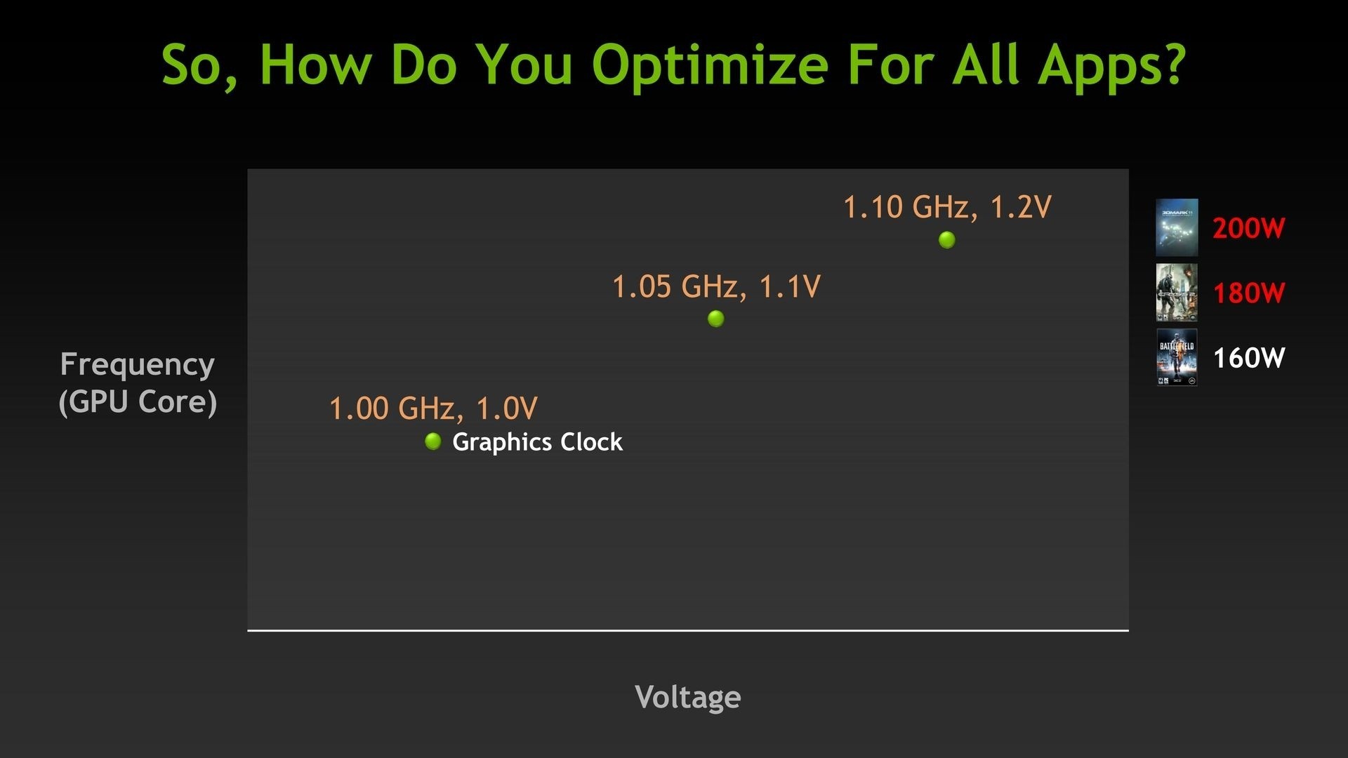
Kepler-based GPUs have a dedicated hardware circuitry that monitors the various aspects of the graphics card, including the power consumption, temperatures, utilization, and so on. The GPU Boost algorithm processes all these inputs to determine the appropriate voltage and frequency headroom. In practical terms, the GPU will dynamically increase the clock frequency when there is sufficient power headroom.

With Kepler and GPU Boost 1.0, NVIDIA also changed how it reports GPU frequencies to the customer. Instead of having a single fixed clock frequency for 3D applications, with GPU Boost 1.0, we have two different clock speeds: the Base Clock Frequency and the Boost Clock Frequency.
- The base clock frequency is the guaranteed minimum GPU frequency during full load workloads. It is equivalent to the traditional GPU clock.
- The boost clock frequency is the GPU’s average clock frequency under load in many typical non-TDP applications that require less GPU power consumption. In other words, the Boost Clock is a typical clock level achieved running a typical game in a typical environment.
The maximum boost clock frequency is … undefined, really. Well, kind of undefined.
Every GPU comes with a factory-fused voltage-frequency curve with a 12.5mV and 13 MHz granularity. This curve defines the relationship between the operating voltage and operating frequency. Depending on the power headroom, the GPU Boost algorithm will select the appropriate point on the voltage-frequency curve. The advertised Boost Clock Frequency indicates where the algorithm lands in a typical scenario.
According to AnandTech’s tests, while the advertised boost clock frequency of the GeForce GTX 680 is 1058MHz, the GPU has a peak frequency of 1110 MHz.
While the power headroom primarily drives the GPU Boost 1.0 algorithm, the GPU temperature still plays a minor role. AnandTech reports that the GTX 680 only achieves a peak frequency of 1110 MHz if the GPU temperature is below 70 degrees Celsius. When the GPU exceeds this temperature threshold, the GPU backs off to the previous point on the voltage-frequency curve.
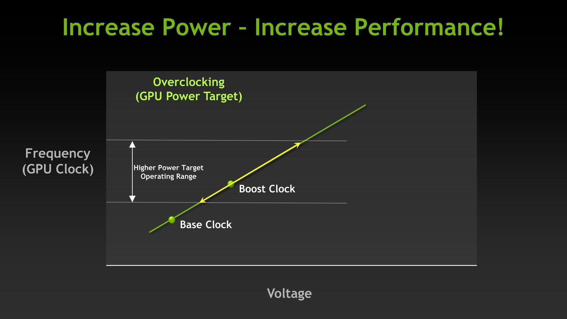
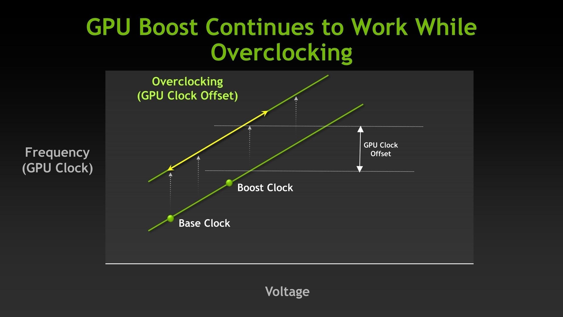
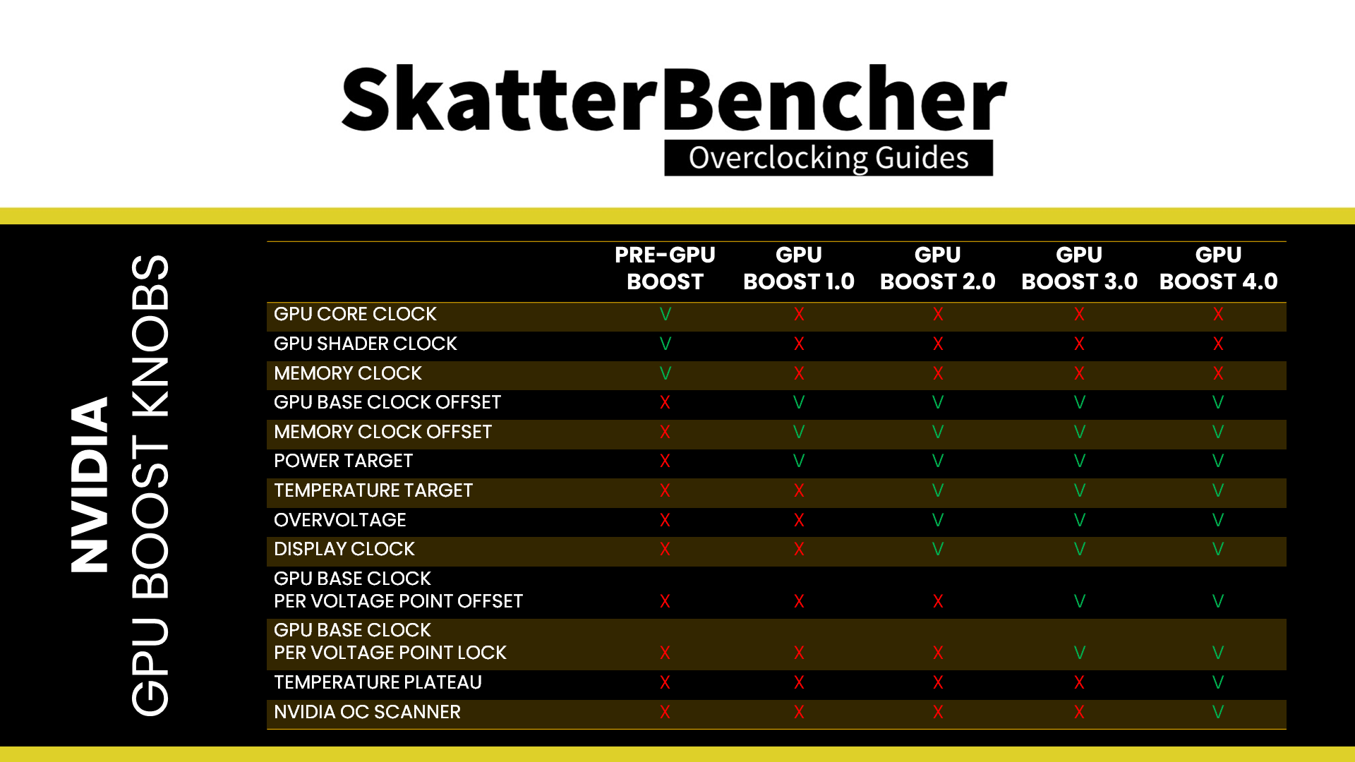
This new approach to GPU clocking also introduces a new approach to overclocking. Rather than setting a fixed voltage and fixed frequency for 3D workloads, overclocking is now all about adjusting the GPU Boost algorithm parameters. GPU Boost 1.0 provides us access to the following overclocking parameters:
- Power target %
- GPU Base Clock Offset
- Memory Clock Offset
The Power Target is a bit of an odd parameter as it is not the same as the TDP. The target isn’t published, but NVIDIA told AnandTech it is 170W for the GeForce GTX 680, below the TDP of 195W. GPU Boost 1.0 allows an increase of up to 32% over the standard Power Target when overclocking the GTX 680. That allows the GPU to boost to higher frequencies even in the most strenuous workloads.
The GPU Base Clock Offset offsets the voltage-frequency curve by a certain amount. If your base frequency is 1000 MHz and your peak frequency is 1100 MHz, with a 200 MHz offset, your new base and peak frequency become 1200 MHz and 1300 MHz. Do note it only changes the frequency of a given V/F Point and not the voltage associated with that V/F Point.
The Memory Clock Offset simply adds an offset to the default memory frequency, similar to how GPU Base Clock Offset works.
If anyone is wondering: voltage control is indeed missing from GPU Boost 1.0. NVIDIA still allows for a dynamic voltage that changes depending on the load; however, the maximum voltage is capped to a Vrel or reliability voltage. That value is determined by NVIDIA and reflects the highest voltage the GPU can safely run at without any impact on lifespan.