Arrow Lake P-core Overclocking

We have a closer look at tuning the performance of the the Arrow Lake P-core, located on the Compute Tile.
Arrow Lake is Intel’s revolutionary new processor for mainstream desktop, featuring new P-cores and E-cores, disaggregated tile-based 3D Foveros packaging, an integrated NPU for AI acceleration, a next-generation uncore, DLVR power rails, and so much more.

In this blog post series, I have a closer look at Arrow Lake and explore its performance tuning and overclocking opportunities. I will cover the Compute (P-core, E-core, Graphics, NPU), Memory Subsystem (DDR, MC), and Data Fabric (Ring, NGU, D2D).
Arrow Lake P-core: Introduction
The Arrow Lake P-cores are located on the Compute Tile which is manufactured using the TSMC N3 process. It shares the tile with the E-cores, the Ring, and the caches.

An Arrow Lake-S processor can have a maximum of eight (8) P-cores, like on the Core Ultra 9 285K. The P-cores feature the Lion Cove micro-architecture, similar to Lunar Lake. Unlike any previous Intel Core architecture, the P-core does not have hyper-threading.

Arrow Lake P-core: Clocking
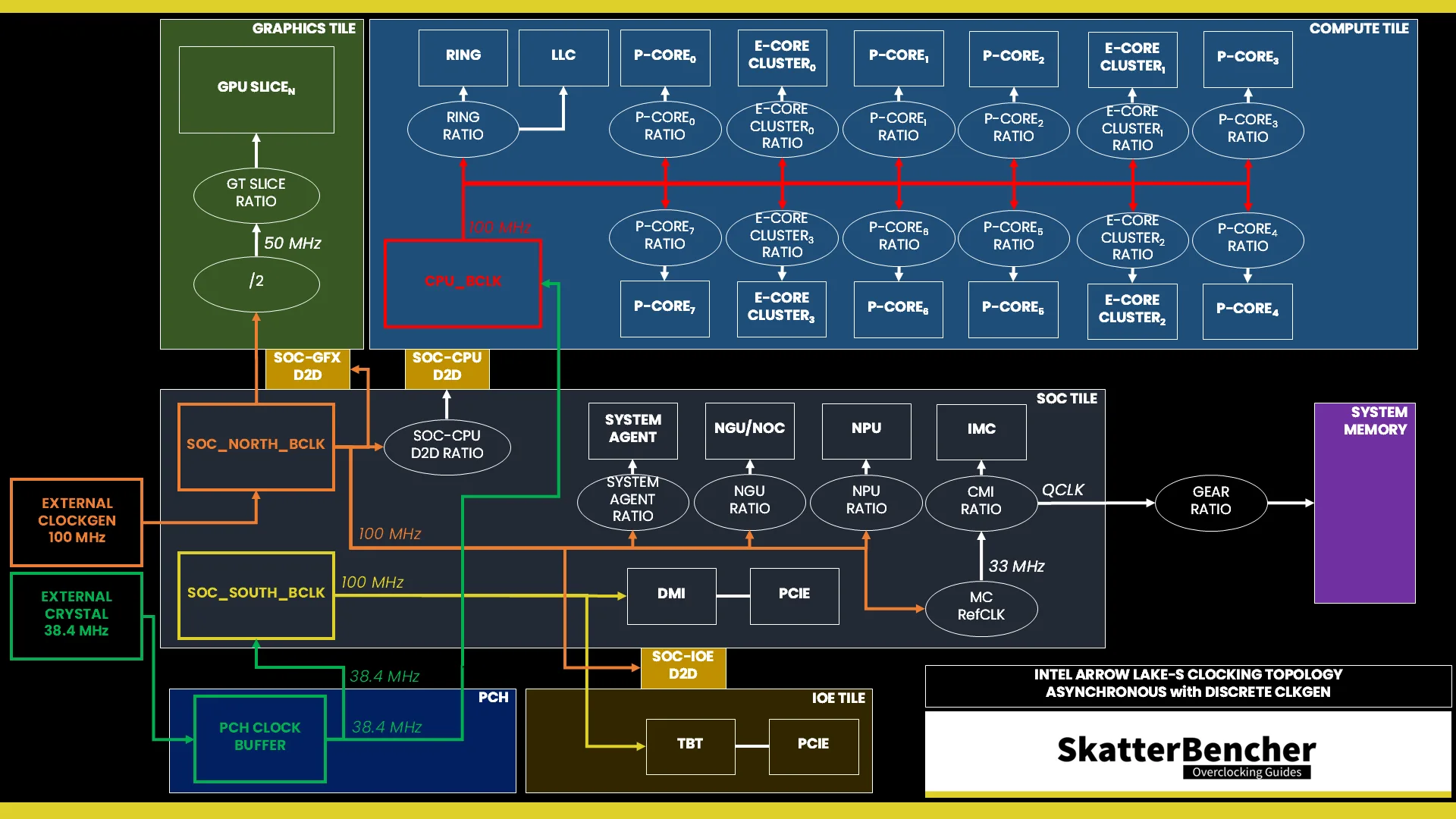
The clocking of the P-cores is similar to previous architectures: a reference clock is multiplied with a ratio to achieve the eventual operating frequency.


Reference Clock
The 100 MHz reference clock frequency is generated internally by the CPU PLL. This clock affects all IP blocks in the Compute Tile, including the P-cores, E-cores, and Ring. This PLL can be linked to the SoC PLL when you run in synchronous mode or work independently if you run in asynchronous mode.
You can configure the CPU BCLK frequency between 40 and 1000 MHz.
In the ASUS ROG BIOS, you can configure the CPU BCLK Frequency in the Ai Tweaker menu by first setting the Ai Overclock Tuner option to anything else than Auto.

You can switch between Asynchronous and Synchronous mode by adjusting the BCLK mode option.

P-Core Ratio
The reference clock is multiplied by the P-core CPU ratio to achieve the final clock frequency. Each P-core can run at an independent clock frequency.
The effective P-core CPU Ratio is determined by three key inputs: the (adjusted) Turbo Ratio Limit, the (adjusted) Per Core Ratio Limit, and the Core Minimum Ratio. The final CPU ratio is determined by the following formula: Max(MIN(aTRL,aPCRL), CMR).

Let’s have a look at each of these technologies.
Turbo Ratio Limit
Generally speaking, there are two ways to manually configure the P-core ratio on Intel platforms: sync all cores or use the Turbo Ratio Limit configuration.
- Sync All Cores sets a single fixed ratio applied to all cores. This is the historical method to get a static overclock.
- Turbo Ratio Limit configuration allows us to modify the default Intel frequency specification and configure a dynamic overclock.
On the Core Ultra 9 285K, the P-core Turbo Ratio Limit starts from 37X, which is the same as the advertised P-core base clock frequency. By default, the P-cores of this SKU can clock up to 5.7 GHz for up to 2 active P-cores and 5.4 GHz for up to all eight active P-cores.

We can configure eight different scenarios: from one to eight active P-cores. Each scenario is associated with a Turbo Ratio Limit. There’s a fixed logic ensuring the ratio for scenario n must be higher than the ratio for scenario n+1.
For example, we can create a scenario where 1 P-core boost to 5.8 GHz, 5 P-cores boost to 5.6 GHz, and when all eight P-cores are active they boost to 5.5 GHz.
The P-core Turbo Ratio Limit configuration works independently from the E-core configuration. So, even if all E-cores are active, if only one P-core is active then its frequency will be set to 5.8 GHz.
The maximum Turbo Ratio Limit is 85X or 120X depending on whether Core Ratio Extension is enabled.
In the ASUS ROG BIOS, you can configure the P-core Turbo Ratio Limit via the Ai Tweaker main menu by setting Performance Core Ratio to By Core Usage.

Per Core Ratio Limit
Per Core Ratio Limit allows you to set a maximum CPU Ratio for every P-core individually. It is an extension of the Intel Turbo Boost Max 3.0 technology introduced in 2016. It acts independently from the Turbo Ratio Limit, meaning that when you set a Per Core Ratio Limit, the P-core ratio will be restricted even if the Turbo Ratio Limit allows for a higher boost frequency.
The Per Core Ratio Limit plays an important role in the Arrow Lake overclocking process. It’s not only the ratio used in the V/F point configuration but also the ratio referenced by many other ratio tuning technologies.
The maximum Per Core Ratio Limit is 80X or 120X depending on whether Core Ratio Extension is enabled.
In the ASUS ROG BIOS, you can configure the Per P-core Ratio Limit via the Ai Tweaker Specific Performance Core sub-menu.

Thermal Turbo (Thermal Velocity Boost)
Thermal Turbo – previously known as Thermal Velocity Boost – is an Intel technology that clips the Turbo Ratio based on the operating temperature. It leverages the same configuration methods as OCTVB which we’ll discuss later in this blog post.
The principle is simple: when the operating temperature exceeds a predefined threshold, the Turbo Ratio Limit will be clipped. In the example of the Core Ultra 9 285K, we find that for 2-active P-cores to 8-active P-cores, the Turbo Ratio Limit is reduced by 1 bin when the operating temperature is over 70 degrees Celsius.

To optimize the performance, we can disable this behavior in the BIOS.
In the ASUS ROG BIOS, you can configure the Thermal Turbo setting via the Ai Tweaker Thermal Velocity Boost sub-menu using the eTVB option.

Core Minimum Ratio
The Core Minimum Ratio is a brand-new feature for Arrow Lake. It allows you to set a CPU ratio floor for the P- and E-cores. The floor value is still defined within the P-states, so it doesn’t prevent the cores from reducing their clock frequency in lower C-states when idling.
In other words, it’s not a replacement for disabling C-states in case you want to prevent core parking or cores from going to sleep.
In the ASUS ROG BIOS, you can configure the Minimum Turbo Ratio via the Ai Tweaker Tweaker’s Paradise sub-menu.

Granular Ratios
Granular Ratios are a brand-new overclocking feature for Arrow Lake. It adjusts the Per Core Ratio Limit by letting you set the CPU frequency in steps of 16.67 and 33.33 MHz. The granular ratios can only be configured in reference to the Per Core Ratio Limit, not as a Turbo Ratio limit. That’s because, technically, the granular ratios aren’t set directly but instead “down-binned” from the Per Core Ratio Limit. So, effectively, setting a granular ratio gives you an “adjusted Per Core Ratio Limit.”

For example, let’s say you set a granular ratio of 60.16X. In that case, the Per Core Ratio Limit is set to 61X and then “down-binned” by 5 steps of 16.67 MHz (100 MHz divided by 6). That is important to keep in mind in case you’re also using other ratio configuration technologies.
In theory, you can set up to 255 down-bin steps from the Per Core Ratio Limit. That can lead to errors in the software reading. Let’s say you set the Per Core Ratio Limit to 60X and then down-bin 200 steps of 16.67 MHz. Then, the operating frequency would be 2667 MHz instead of 6000 MHz.

Fortunately, you’ll find that most BIOSes give you a simple interface to set granular ratios.
In the ASUS ROG BIOS, you can configure the P-core Granular Ratio via the Ai Tweaker Specific Performance Core sub-menu.

OverClocking Thermal Velocity Boost
OverClocking Thermal Velocity Boost (OCTVB) allows us to reduce the CPU ratio at specified operating temperatures. While OCTVB is not new for Arrow Lake, the feature has expanded in functionality.
We can now configure the OCTVB based on the “Per CCP Module” or “Per P-core Group.” Perhaps an easier way to think about this is that the former adjusts the Per Core Ratio Limit, and the latter adjusts the Turbo Ratio Limit. The latter is functionality carried over from previous generations whereas the former is new for Arrow Lake.

In “Per CCP Module” mode, each P-core has two available OCTVB points. Each point is defined by a target temperature and a number of down-bins. The temperature can be defined anywhere between 1 and 115 degrees Celsius. The down-bins can be defined between 0 and 31. Note that the down-bins are cumulative and thus the down-bins from point B stack on top of the down-bins from point A.
For example, let’s say we’ve set the P-core 0 Per Core Ratio Limit to 60X, and set the “Per CCP Module” OCTVB Point A to -2X at 50C and OCTVB Point B to -2X at 80C. In that case, the frequency will be 6 GHz below 50C, 5.8 GHz between 50C and 80C, and 5.6 GHz above 80C.

The OCTVB trigger point is the core-specific temperature. So, even if all other cores exceed the P-core’s OCTVB temperature point, as long as that specific P-core’s temperature does not exceed the target temperature, it will not down-bin.
In the ASUS ROG BIOS, you can configure the Overclocking Thermal Velocity Boost Per CCP Module via the Ai Tweaker Thermal Velocity Boost sub-menu by first enabling Overclocking TVB and then setting OC TVB Configuration Limit to Per CCP Module.

In “Per P-core Group” mode, each P-core Turbo Ratio Limit scenario has two available OCTVB points, each of which is defined by a target temperature and a number of down-bins. The temperature can be defined anywhere between 1 and 115 degrees Celsius. The down-bins can be defined between 0 and 31. Note that the down-bins are cumulative and thus the down-bins from point B stack on top of the down-bins from point A.
For example, let’s say we’ve set the Turbo Ratio Limit for 2 active P-cores to 60X, and set the “Per P-core Group” OCTVB Point A to -2X at 50C and OCTVB Point B to -2X at 80C. In that case, when 2 P-cores are active, the frequency will be 6 GHz below 50C, 5.8 GHz between 50C and 80C, and 5.6 GHz above 80C.

In the ASUS ROG BIOS, you can configure the Overclocking Thermal Velocity Boost Per P-core Group via the Ai Tweaker Thermal Velocity Boost sub-menu by first enabling Overclocking TVB and then setting OC TVB Configuration Limit to Per P-core Group.

One last important thing to mention is that, for now at least, the temperature point is 5C off. By that, I mean that if you set the OCTVB point to 55C it actually kicks in at 60 degrees. That may be due to the TjMax increase from 100C on the previous generation Raptor Lake to 105C on Arrow Lake.
AVX Ratio Offset
AVX Ratio Offset enables us to reduce the CPU operating frequency when the workload uses AVX instructions by down-binning a predefined number of Turbo bins from the Per Core Ratio Limit.

AVX Ratio Offsets are useful to achieve maximum performance for both SSE and AVX workloads. The AVX Ratio Offset behavior is managed using a frequency license-based approach. In theory, there are four frequency levels, ranging from L0 for SSE to L3 for AMX workloads. However, on Arrow Lake only licenses L0 and L1 are available since it doesn’t support AVX-512 or AMX instruction sets. Each level is associated with particular instructions ranging from lightest to heaviest. Each level is also associated with one specific ratio offset.
On Sapphire Rapids, the different levels respond to different types of AVX workloads. So, you can find that light AVX2 workloads don’t actually trigger a switch to L1 frequency-license. I haven’t seen any documentation that suggests this works differently on Arrow Lake. As a rule, the ratio offset configured for a given frequency license must be equal to or higher than the preceding frequency license. In other words: L0 = 0 ≤ L1 ≤ L2 ≤ L3.

When the AVX ratio offset is triggered, the Per Core Ratio Limit is temporarily reduced by the number of defined AVX Ratio bins.
In the ASUS ROG BIOS, you can configure the AVX Ratio Offset via the Ai Tweaker AVX Related Controls sub-menu.

Arrow Lake P-core: Voltage
The voltage regulation for the P-cores is more complex than prior generations of Intel Core processors due to the introduction of the DLVRs. The DLVRs enable much lower voltage levels for the P-cores but still rely on a dynamic external motherboard voltage regulator as the input voltage source.


V/F Curve
Each Core Ultra 9 285K P-core has its own V/F curve which is defined by up to nine (9) V/F points. The first eight (8) V/F points are factory-fused, and the last point is mapped to the “OC Ratio.”

Here is the P-core V/F curve for my specific Core Ultra 9 285K. The voltage is about 725 mV at 800 MHz, then increases to 1.17V for VF Point 6 at 5.5 GHz, and ultimately ends at 1.313V for V/F Point 8 at 5.7 GHz.

5.7 GHz is the default maximum turbo frequency for the P-cores. That’s only for the two favored cores, though. The other, non-favored, P-cores only boost up to 5.5 GHz. That said, all P-cores have a V/F curve up to 5.7 GHz. So, if you set the non-favored cores to 5.7 GHZ, they’ll still be running the appropriate factory-fused voltage.

In the ASUS ROG BIOS, you can find an approximation of the P-core’s V/F points (and thus V/F curve) in the Ai Tweaker Performance Core V/F Point Offset sub-menu.

Advanced Voltage Offset (V/F Points)
Advanced Voltage Offset, more commonly known as V/F Points, is available for each of the P-cores. There are nine (9) available VF Points for each P-core, eight of which are fixed to a specific ratio. That ratio is the same for all P-cores.

The final VF Point is mapped to the “OC Ratio” which is the P-core Per Core Ratio Limit. If you use granular ratios, keep in mind those are down-binned from the next full ratio. In other words, the OC Ratio cannot be a granular ratio!
You can set a negative or positive voltage offset for each of these V/F points and for each of the P-cores. The final OC ratio’s base voltage will be the user-configured adaptive voltage.
In the ASUS ROG BIOS, you can configure the P-core V/F Points via the Ai Tweaker Performance Core V/F Point Offset sub-menu.

Voltage Limits
To safeguard the processor, Intel has imposed strict voltage limits for several IP blocks, including the P-cores. This limit effectively prevents P-cores from requesting a higher voltage from the PCU.
By default, the voltage limit for the P-cores is 1.513V, but this can be increased to 1.610V under ambient conditions. When the temperature is below 10 degrees Celsius, you can further increase the voltage limit or disable the limit altogether.
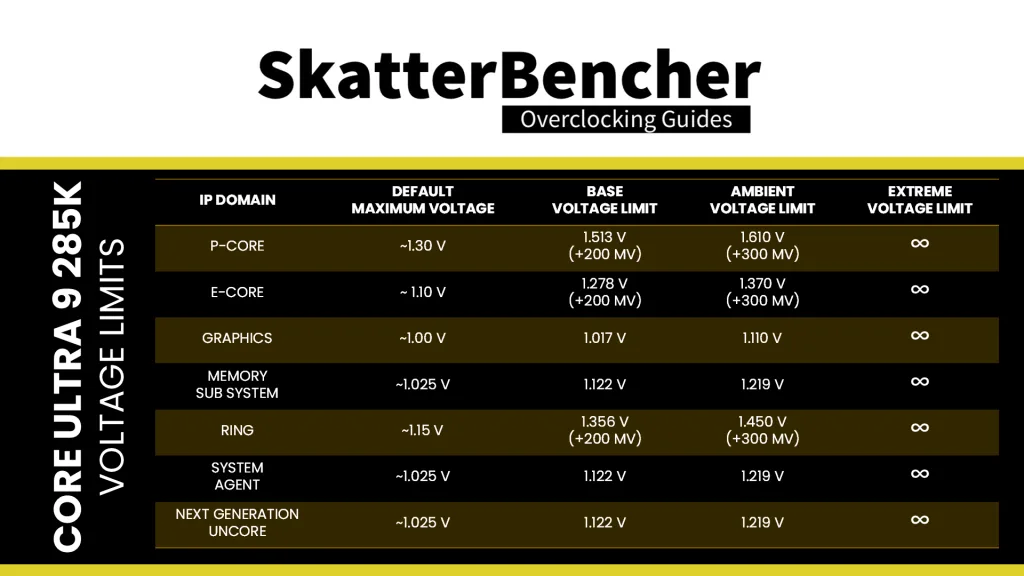
If you try setting the limit above the approved limit, the PCU will automatically adjust it to the highest allowed limit. If you disable voltage limits and the temperature is above 10 degrees Celsius, the CPU will operate in “safe mode” and limit the frequency to 400 MHz.
For DLVR-powered IP blocks like the P-cores, in theory, you can also change to PG mode to override the voltage limit and set any voltage you want. Of course, motherboard vendors can implement their own voltage limits for the voltage regulator.
In the ASUS ROG BIOS, you can configure the P-core Voltage Limit via the Ai Tweaker Max Voltage Limits sub-menu.

Thermal Velocity Boost Voltage Optimizations
Thermal Velocity Boost is an Intel technology that exploits the fact that CPUs need less voltage to run a specific frequency when the operating temperature is lower. When this technology is enabled, the CPU automatically adjusts the operating voltage according to the operating temperature. If you want manual control over the operating voltage to ensure stability, it’s prudent to disable this function.
When the voltage optimizations are enabled, we can use HWiNFO to track the CPU VID request as the CPU heats up. I’ve collected data for the Core Ultra 9 285K to illustrate this behavior. As you can see from the data, with the P-core at 5.4 GHz, the operating voltage is 1.237V when the temperature is below 50 degrees Celsius. However, it increases to nearly 1.3V when the temperature approaches 100 degrees Celsius.

A regression analysis tells us that the operating voltage changes 1.1 mV for every change in degree Celsius.

In the ASUS ROG BIOS, you can enable or disable the Thermal Velocity Boost Voltage Optimizations via the Ai Tweaker Thermal Velocity Boost sub-menu.

VccIA MBVR
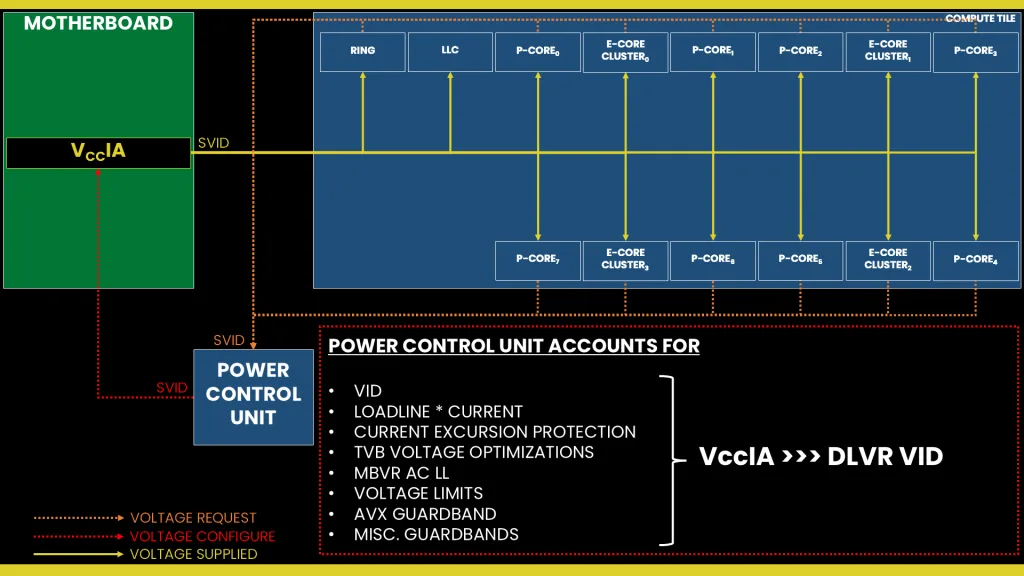
The external VccIA motherboard voltage regulator (MBVR) provides the input voltage for the individual P-core, E-core clusters, Ring, last-level cache (LLC), and E-core L2 cache. Each P-core, E-core cluster, and Ring has an individual Digital Linear Voltage Regulator (DLVR) between the VccIA rail and the IP blocks. That means each of the blocks can operate at its own voltage.
- VccCOREn is the DLVR powering an individual P-core.
- VccR is the DLVR powering the Ring and Last-Level Cache.
- VccATOMn is the DLVR powering an individual E-core cluster, which consists of four E-cores, and its L2 cache.
The DLVRs can also be bypassed. In that case, the IP blocks are running in so-called Power Gate (PG) mode. In PG mode, the VccIA voltage rail directly powers the IP blocks, and they all share the same voltage. That’s similar to how previous generations of Intel CPU architecture worked.
The default mode of operation is DLVR mode. Let’s explore that first.
VccCOREn DLVR Mode
Based on the VF curve, the P-cores request an operating voltage using the SVID protocol from the CPU Power Control Unit (PCU).

The PCU in turn configures the VccIA voltage rail and the individual VccCOREn DLVRs. There are two ways to configure the P-core voltage:
- Adaptive mode is the standard mode of operation, which relies on the factory-fused voltage-frequency curves we discussed before.
- Override mode specifies a single static voltage across all ratios. It is mainly used for extreme overclocking where stability at high frequencies is the only consideration.
We can configure override and adaptive modes directly in the PCU by specifying a target voltage and a voltage offset for each mode.
In adaptive mode, the target voltage is mapped to a P-core’s “OC Ratio.” Each P-core has its own “OC Ratio” which is defined by the Per Core Ratio Limit. This also matches the P-core VF Point 9. You can configure the adaptive voltage and OC Ratio to any value, however, multiple rules enforce what ratio and voltage are actually set.

Rule #1: the voltage set for a given VF Point n must be higher than or equal to the voltage set for VF Point n-1.
In the case of the P-core, it means that the voltage for the OC Ratio, matching V/F Point 9, must be higher than or equal to the voltage for VF Point 8. This can be a little strange because you can program the OC ratio to any value, including lower than 57X (V/F Point 8).
For example, let’s say you set the P-core Per Core Ratio Limit to 52X and the adaptive voltage to 1.1V. In that case, VF Point 9 will be programmed to 52X at 1.1V. However, the actual frequency will be 5.2 GHz with 1.313V, as that’s the voltage for VF Point 8.

Rule #2: for ratios between the OC Ratio and the next highest factory-fused V/f point, the voltage is interpolated between the set adaptive voltage and the factory-fused voltage.
Let’s say we configure the P-core VF OC Point to 60X and 1.40V. The target voltage for P-core ratios between 57X and 60X is now interpolated between the factory-fused voltage for 57X and the set adaptive voltage for 60X.

In the ASUS ROG BIOS, you can configure the P-core DLVR Voltage in the Ai Tweaker menu. You can configure it in adaptive, manual, and offset mode.

I have two additional sidenotes about adaptive voltage.

First, the adaptive offset is applied across the entire curve. So, if we set +100 mV adaptive offset, the operating voltage for all frequencies between 8X and the OC ratio will be increased by 100 mV.
Second, any adjustments made to the V/F curve are still subject to the aforementioned rules for adaptive voltage. That includes the adjustments for the V/F Points.
For example, let’s say the P-core 0 voltages for V/F Points 7 and 8 are 1.2V and 1.3V respectively. If I configure a -150 mV offset for V/F Point 8, then the effective voltage will be 1.2V, not 1.15V, because adaptive voltage Rule #1 is enforced.

Per Core Voltage
Intel Per Core Voltage allows you to set a specific target voltage for every individual P-core inside your CPU. The tool is an extension of DLVR mode as it only works when DLVR is enabled.
Just like in DLVR mode, you can configure the Per Core Voltage in adaptive mode and override mode, specifying a voltage for the defined Per Core Ratio Limit or across the V/F curve respectively.
The Per Core Voltage implementation for Arrow Lake is slightly different than prior platforms as each P-core now has its own “OC Ratio.” Functionally, that means each P-core’s Per Core Voltage is mapped to its Per Core Ratio Limit and, thus, also serves as the base voltage for V/F Point 9.
The standard rules for adaptive voltage mode still apply for each P-core. As a consequence, it means that each P-core’s V/F curve is truly independent as voltage interpolation is done for each P-core individually.
Let’s say we configure the P-core 1 VF Point 9 to 60X and 1.40V and we set P-core 2 VF Point 9 to 61X and 1.45V. The target voltage for P-core 1 ratios between 57X and 60X is now interpolated between the factory-fused P-core 1 voltage for 57X and 1.4V for 60X. For P-core 2, the ratios between 57X and 61X are interpolated between the factory-fused P-core 2 voltage for 57X and 1.45V for 61X.

In the ASUS ROG BIOS, you can configure the Per P-core DLVR Voltage in the Ai Tweaker Specific Performance Core sub-menu. You can configure it in adaptive, manual, and offset mode.

VccIA Power Gate SVID Mode
In Power Gate Mode, all the DLVRs tied to the VccIA voltage rail are bypassed and the connected IP blocks are powered directly by the VccIA voltage rail. That includes the P-cores, E-core clusters and their cache, the Ring, and the last-level cache.
Power Gate mode is basically how the VccIA rail worked on previous generation Raptor Lake processors. For Arrow Lake, it works … but it’s a little complicated.
To make a long story short: when the P-cores, E-cores, and Ring request their voltage to the CPU PCU, they account for a ton of other compensations including voltage droop, AVX Guardband, Thermal Velocity Boost voltage optimizations, etc. The result is that the actual voltage provided from the VccIA voltage rail to the IP blocks is relatively high!
For example, here are the voltages with the CPU at stock voltage and frequency (P53X, E46X, R39X) running a light all-core workload:
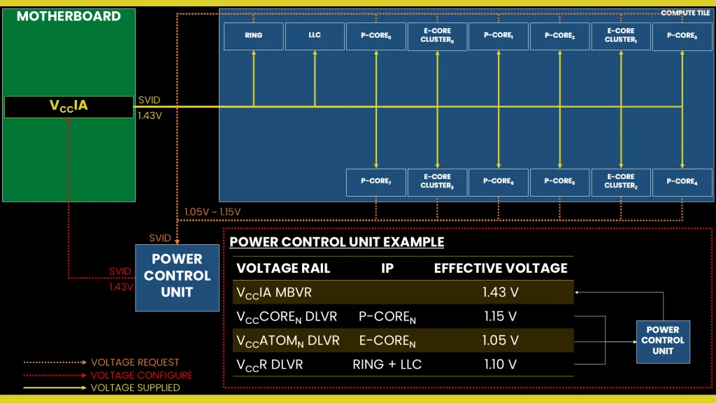
We can interpret this as follows: the P-core, E-core, and Ring request a voltage to the PCU to ensure it’ll run at 1.15V, 1.05V, and 1.1V respectively. The PCU then adds compensation for the loadlines, CEP, TVB, AVX, AC LL, DLVR efficiency losses, etc. At the end of the calculation, the PCU determines the VccIA voltage rail should provide 1.43V input voltage to the DLVRs.
If we were to switch to Power Gate mode but maintain the same mechanism for calculating the required voltage, then the VccIA voltage rail would effectively provide 1.43V to the P-cores, E-cores, and Ring. That’s obviously way too high for the target frequency and would quickly result in an overheating system. But this would be how voltage was configured on previous-generation Raptor Lake processors.
VccIA Power Gate PMBus Mode
Fortunately, there’s another way to approach Power Gate Mode voltage configuration: ignore the SVID voltage requests and calculations, and program the VccIA voltage regulator directly using PMBus. This process effectively allows us to take full control over the voltage set by the VccIA voltage rail.
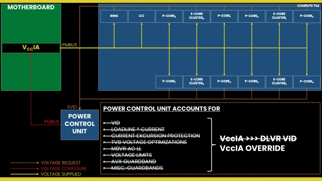
This approach is a very traditional way of overclocking whereby you set a fixed output voltage and use an appropriate VRM loadline setting to reduce the operating voltage in higher load scenarios.
Let’s have a look at an example and compare Power Gate and DLVR in Cinebench R23.
If we set 1.35V with LLC=6, then the effective voltage under load is 1.26V. That’s about 150mV higher than with DLVR. Despite the higher voltage, the temperature is only 7C higher than when we ran DLVR.
If we set 1.30V with LLC=4, then the effective voltage under load is 1.15V which is very similar to DLVR. Despite the almost identical voltage, the temperature is 7 degrees Celsius lower than with DLVR.
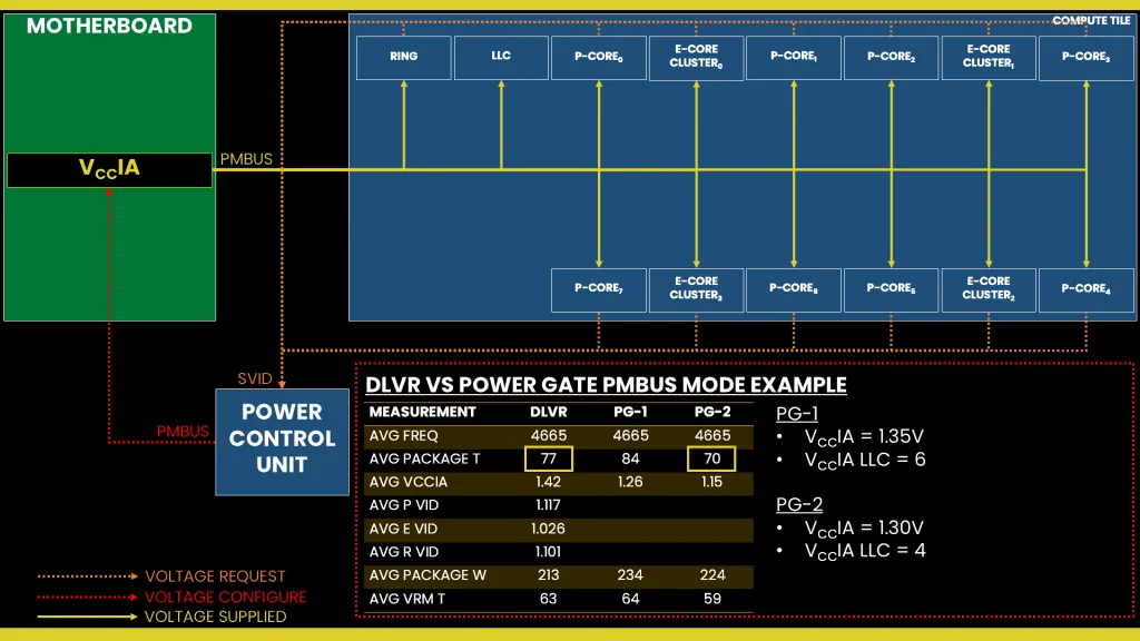
The bottom line on DLVR versus PG mode is that DLVR seems to provide better temperatures and efficiency in low-load scenarios because it can have the P-core run at lower voltage. However, in high-load scenarios where the total current exceeds 150A, the power loss associated with the linear voltage regulator translates into a not-insignificant increase in temperature, which eats into the thermal budget of our thermal solution and, ultimately, lowers the overclocking headroom.
How much exactly? Well, the power loss across a linear voltage regulator equals the decrease in voltage across the DLVR multiplied by the total load.
In our example, with a voltage drop of 305mV and 160A load, the power loss is 48.8W. Nearly all of that power loss will convert into heat.

For high-load scenarios, PG mode appears to offer better overclocking headroom because the operating temperature is lower. However, we cannot rely on the PCU to control the VccIA output voltage because its calculations are too conservative. So, it ends up overvolting too much.
Therefore, the right way of overclocking using PG mode is to ignore the SVID requests entirely and take direct control of the VccIA voltage regulator. This also requires setting an appropriate VR loadline to ensure lower voltage in all-core workloads.
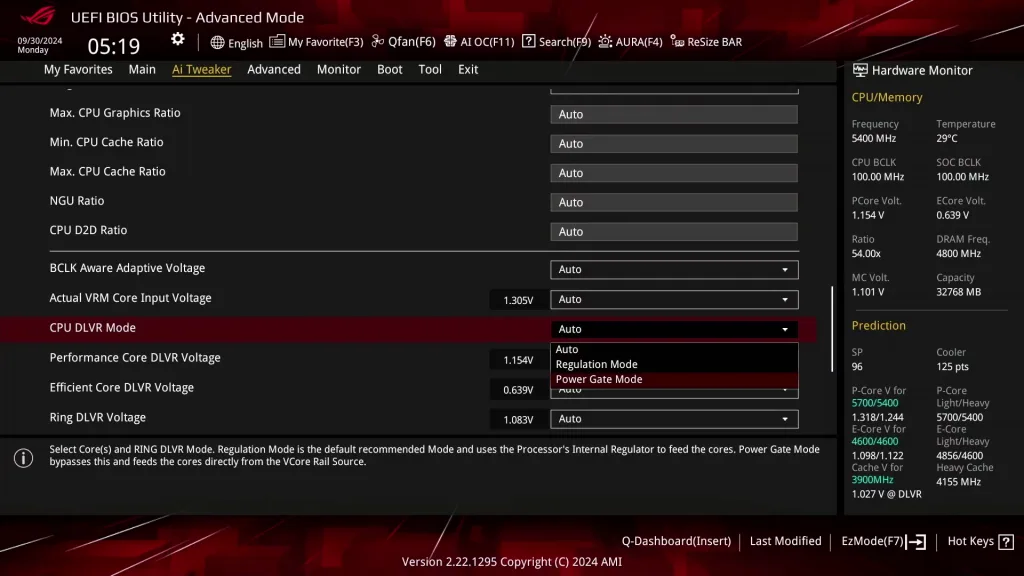
In the ASUS ROG BIOS, you can switch between DLVR and Power Gate mode for the VccIA voltage rail in the Ai Tweaker menu by configuring the CPU DLVR Mode menu item.
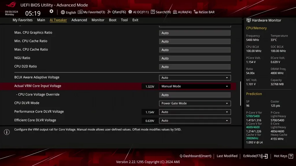
In the ASUS ROG BIOS, you can set the VccIA voltage rail in the Ai Tweaker menu by configuring the Actual VRM Core Input Voltage in manual mode.
Arrow Lake P-core: Power
The processor power consumption is primarily governed by the Turbo Boost 2.0 Technology.
Turbo Boost 2.0 Technology
Intel Turbo Boost 2.0 Technology allows the processor cores to run faster than the base operating frequency if the processor is operating below rated power, temperature, and current specification limits. The ultimate advantage is opportunistic performance improvements in both multi-threaded and single-threaded workloads.
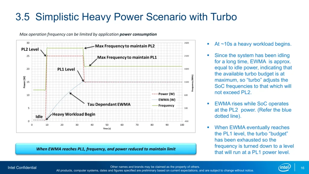
The turbo boost algorithm works according to an EWMA formula. This stands for Exponentially Weighted Moving Average. There are three main parameters to consider: PL1, PL2, and Tau.
- Power Limit 1, or PL1, is the threshold that the average power will not exceed. Historically, this has always been set equal to Intel’s advertised TDP. Very importantly, PL1 should not be set higher than the thermal solution cooling limits.
- Power Limit 2, or PL2, is the maximum power the processor is allowed to use for a limited amount of time.
- Tau is a weighing constant used in the algorithm to calculate the moving average power consumption. Tau, in seconds, is the time window for calculating the average power consumption. If the average power consumed is higher than PL1 the CPU will reduce the CPU frequency.
Turbo Boost 2.0 Technology has evolved over the past years to incorporate a lot of power, thermal, and electrical performance limiters, including PL3, PL4, IccMax, TCC_Offset, VR_TDC, RATL, Pmax, and many more. To cover each in this guide would take up too much time.
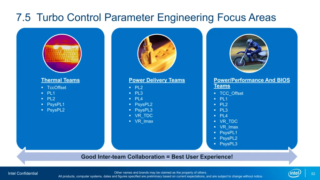
Fortunately, Intel provides two performance profiles for the Arrow Lake SKUs which configure all these settings for you. For the Core Ultra 9 285K, the Turbo Boost 2.0 profiles are Performance and Extreme.
In the ASUS ROG BIOS, you can switch between Intel Default Performance Profiles in the Ai Tweaker menu by setting the Performance Preference menu item to Intel Default Settings and selecting one of the two Intel Default Settings options.
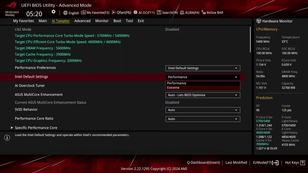
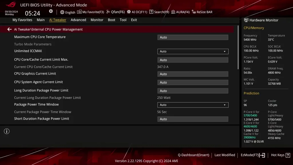
Should you wish to override the performance profiles, you can do so in two ways: either by manually configuring them in the BIOS or by enabling ASUS Multi-Core Enhancement.
In the ASUS ROG BIOS, you can find many Turbo Boost 2.0 parameter options in the Ai Tweaker Internal CPU Power Management sub-menu.
ASUS MultiCore Enhancement
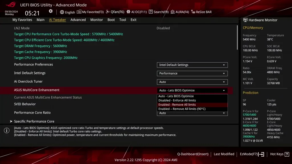
ASUS MultiCore Enhancement enables higher out-of-the-box performance for heavy, power-hungry, multi-threaded workloads. It does this by optimizing the Turbo Boost 2.0 configuration. There are four available options.
- Auto, let the ASUS motherboard decide.
- Disabled – Enforce All Limits, following the Intel guidelines for Turbo Boost 2.0 power and ratio configuration
- Enabled – Remove All Limits, unleashes the Intel Turbo Boost 2.0 power limits for maximum performance.
- Enabled – Remove All Limits (90C), unleashes the Intel Turbo Boost 2.0 power limit but restricts the maximum CPU temperature to 90 degrees Celsius.
Note that you can select an Intel Performance Profile and enable MCE at the same time. The effect will be that MCE overrides the most common Turbo Boost 2.0 parameters such as PL1 and PL2, but will adhere to other limiters such as Current Excursion Protection (CEP) configured by the Intel Performance Preset.
In the ASUS ROG BIOS, you enable ASUS MultiCore Enhancement in the Ai Tweaker menu.
ASUS Advanced OC Profile
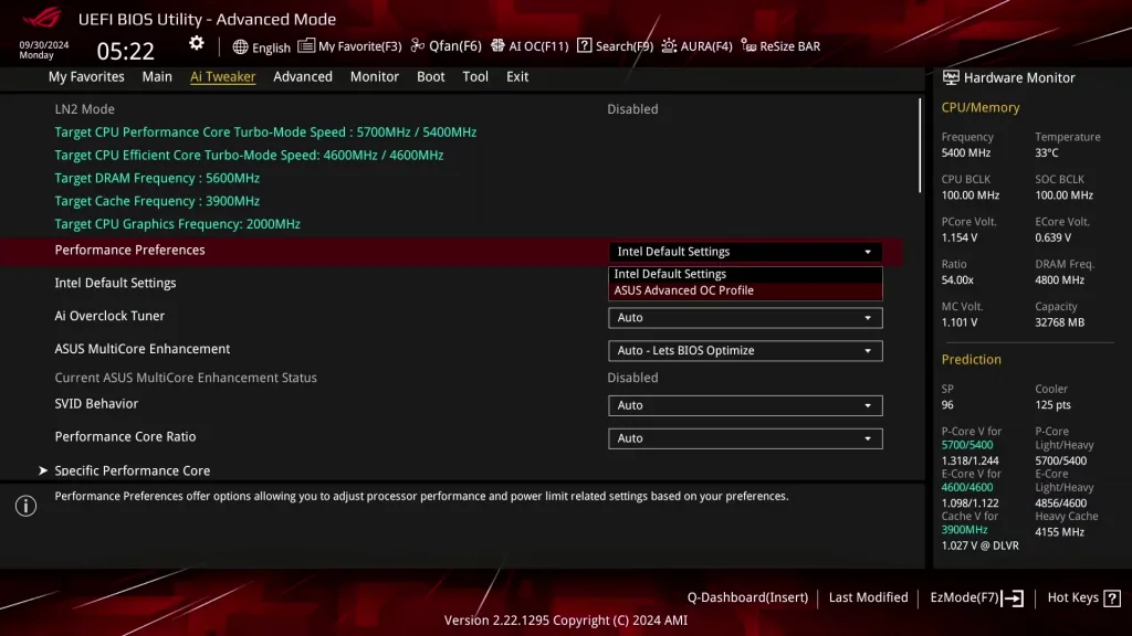
The ASUS Advanced OC Profile is a more elaborate unleashed overclocking profile than MultiCore Enhancement as it not only adjusts the major Turbo Boost 2.0 parameters but also implements a lot of BIOS auto-rules to facilitate overclocking.
In the ASUS ROG BIOS, you can switch to the ASUS Advanced OC Profile in the Ai Tweaker menu by setting the Performance Preference menu item.
Arrow Lake P-core: Overclock & Undervolt
Overclocking the P-cores is pretty similar to how it was on Raptor Lake. Its total impact on performance compared with the E-cores is less than it was on Raptor Lake. That’s in part due to the lack of hyper-threading and in part to the significant improvement in performance and clock frequency of the E-cores. So, contrary to previous platforms, on Arrow Lake it’s a good idea to prioritize E-core performance tuning since it typically gives the best performance enhancement. Especially in all-core workloads.
Let’s compare the performance improvement in Cinebench R23, changing the P and E-core clock from 4.6 to 5.0 GHz. The performance improvement from overclocking the 4 E-core clusters is about twice that from overclocking the 8 P-cores.

The P-core overclocking range is also somewhat limited.
While all P-cores could do 5.8 GHz, only few could make it to 5.9 GHz. That was with a quick OCCT stability test, so I wouldn’t expect this to actually work for a daily overclock.

I also tried leveraging OCTVB to achieve 6 GHz, but I couldn’t quite make that work stable either.

In an all-core scenario, I achieved 5.7 GHz in a light all-P-core SSE workload such as Y-Cruncher BKT. However, in a heavy workload like Cinebench, which uses AVX instructions that don’t trigger the AVX offset, the maximum P-core frequency is about 5.5 GHz

The undervolting margin seems to be pretty decent too. I could undervolt about 100mV for the P-cores at 5.4 GHz in an all-core workload.
Daniel
Hi. Because I’m a curious guy, no words about preferred cores and how they are defined from factory and how different they work?
265K guide coming?
MQB888R
Greetings. Thank you for the great content.
When overclocking P Cores, what approach should I take to voltage regulation (fixed, adaptive, offset, DLVR, OCTVB, etc.) and to core ratios? You discuss several approaches, I am curious which is the most effective and which is the most efficient for a stable 24/7 OC?
The last platform I overclocked was Z390, so I am catching up. Thank you.
Pieter
I don’t have a good answer for you yet as I’m still working on my Arrow Lake overclocking guides.
Hopefully by the end of writing those guides I’ll be able to tell what’s the best approach.