SkatterBencher #74: AMD Ryzen 5 8500GE Overclocked to 5225 MHz

We overclock the AMD Ryzen 5 8500GE to 5225 MHz with the ASUS ROG Crosshair X670E Hero motherboard and custom loop water cooling.
This is the third Hawk Point APU I overclocking on this channel, following the Ryzen 7 8700G and Ryzen 5 8600G. However, this is the first Phoenix 2-based APU I’m overclocking and these have a mix of Zen 4 and Zen 4c cores. Since the chip architecture is so different from a standard monolithic chip, it was very interesting to explore how Zen 4 and Zen 4c cores work together.
In this video, I’ll try to explain how everything works. Hope you enjoy the video!
AMD Ryzen 5 8500GE: Introduction
The Ryzen 5 8500GE is part of AMD’s Zen 4-based Ryzen 8000 desktop APU product line codenamed “Hawk Point” which was introduced on January 8, 2024.
The -GE SKUs were quietly announced a month later. They are the same as their -G counterparts, but rated at 35W instead of 65W. Oddly I can only find the Ryzen Pro version of this CPU on AMD’s website. However, my APU is recognized as a regular non-Pro Ryzen.
Hawk Point is the successor to the Ryzen 5000 Cezanne APUs launched in 2021. There are more than a few differences between these chips. Here’s the shortlist:
- The CPU architecture moves from Zen 3 to Zen 4 and Zen 4c cores, depending on the SKU
- Hawk Point comes with an integrated XDNA AI accelerator
- The chips are produced using the TSMC N4P process
- Hawk Point supports DDR5 (but not PCIe Gen 5)
- The integrated graphics is based on the RDNA 3 architecture.
The Ryzen 8000 series APUs come to market in two distinct configurations. APUs with the Phoenix 1 die only have Zen 4 cores while the APUs with the Phoenix 2 die come with a mix of Zen 4 and Zen 4c cores.

A lot has been said about the difference between Zen 4 and Zen 4c cores. I won’t regurgitate everything here, but the point is that the core architecture is identical while Zen 4c cores have a smaller footprint. The benefit is that you get more compute per area, but the tradeoff is that you also have higher hotspot temperatures and lower frequencies.
In AMD nomenclature, you’ll find that the Zen 4 cores are referred to as the Classic cores (or “C-cores”), and the Zen 4c cores are referred to as the Dense cores (or “D-cores”). Throughout this guide, I will also refer to them accordingly.

To support a mix of Classic and Dense compute cores, the Phoenix 2 clocking and voltage topologies are significantly different from Phoenix 1. I will cover these details in the final overclocking strategy. For now, suffice to know that the C- and D-cores operate at different clock frequencies and they each have different frequency limits.
The Ryzen 5 8500GE has two C-cores and four D-cores cores with 12 threads. The base frequency is 3.4 GHz, and the listed maximum boost frequency is 5.0 GHz. The TDP is 35W, and the TjMax is 95 degrees Celsius.
In this video, we will cover three different overclocking strategies:
- First, we enable Precision Boost Overdrive 2 and enable EXPO.
- Second, we undervolt and overclock using the Precision Boost Overdrive 2 toolkit.
- Lastly, we leverage asynchronous eclk to maximize our CPU overclock.
However, before we jump into overclocking, let us quickly review the hardware and benchmarks used in this video.
AMD Ryzen 5 8500GE: Platform Overview
The system we’re overclocking today consists of the following hardware.
| Item | SKU | Price (USD) |
| CPU | AMD Ryzen 5 8500GE | ~180 |
| Motherboard | ASUS ROG Crosshair X670E Hero | 640 |
| CPU Cooling | EK-Pro QDC Kit P360 | 750 |
| Fan Controller | ElmorLabs EFC-SB | 50 |
| Memory | G.SKILL Trident Z5 DDR5-6400 | 120 |
| Power Supply | Antec HCP 1000W Platinum | 250 |
| Graphics Card | ASUS ROG Strix RTX 2080 TI | 490 |
| Storage | AORUS RGB 512 GB M.2 | 75 |
| Chassis | Open Benchtable V2 | 200 |
ElmorLabs EFC-SB SkatterBencher Edition
In March 2023, I launched the EFC SkatterBencher edition in collaboration with ElmorLabs. The EFC-SB is a customized version of the original ElmorLabs Easy Fan Controller, which I’ve used since SkatterBencher #26. The base product functions and features are the same as the original EFC, with a tiny improvement here and there. The most obvious difference is that this EFC version comes in the SkatterBencher color scheme: yellow, white, and black.

I explained how I use the EFC devices in many previous SkatterBencher guides. I monitor the ambient temperature (EFC), water temperature (EFC), and fan duty cycle (EFC). I include the measurements in my stability test results.
I also use the device to map the radiator fan curve to the water temperature. Without going into too many details, I have attached an external temperature sensor from the water in the loop to the EFC-SB. Then, I use the low/high setting to map the fan curve from 25 to 40 degrees water temperature.
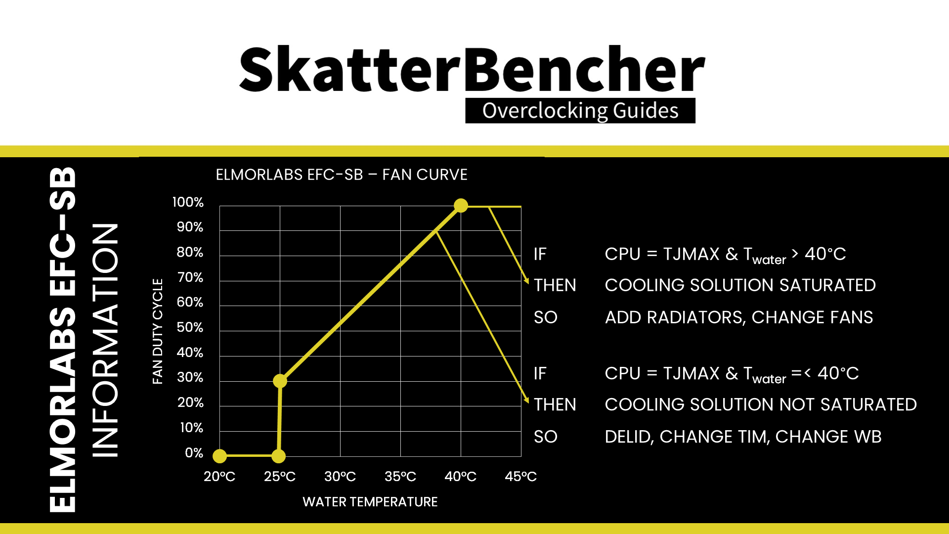
I use this configuration for all overclocking strategies. The main takeaway from this configuration is that it gives us a good indicator of whether the cooling solution is saturated.
AMD Ryzen 5 8500GE: Benchmark Software
We use Windows 11 and the following benchmark applications to measure performance and ensure system stability.
| BENCHMARK | LINK |
| SuperPI 4M | https://www.techpowerup.com/download/super-pi/ |
| Pyprime 2.0 | https://github.com/mbntr/PYPrime-2.x |
| 7-Zip 19.0 | https://www.7-zip.org/ |
| Geekbench 6 | https://www.geekbench.com/ |
| Cinebench 2024.1 | https://www.maxon.net/en/cinebench/ |
| CPU-Z | https://www.cpuid.com/softwares/cpu-z.html |
| V-Ray 5 | https://www.chaosgroup.com/vray/benchmark |
| Corona Benchmark | https://corona-renderer.com/benchmark |
| AI-Benchmark | https://ai-benchmark.com/ |
| Y-Cruncher | http://www.numberworld.org/y-cruncher/ |
| 3DMark CPU Profile | https://www.3dmark.com/ |
| 3DMark Night Raid | https://www.3dmark.com/ |
| Returnal | https://store.steampowered.com/app/1649240/Returnal/ |
| Shadow of the Tomb Raider | https://store.steampowered.com/app/750920/Shadow_of_the_Tomb_Raider_Definitive_Edition/ |
| Final Fantasy XV | http://benchmark.finalfantasyxv.com/na/ |
| OCCT | https://www.ocbase.com/ |
AMD Ryzen 5 8500GE: Stock Performance
Before starting overclocking, we must check the system performance at default settings. The default Precision Boost 2 parameters for the Ryzen 5 8500GE are as follows:
- PPT: 42 W (Fast Limit, Slow Limit, APU Only Limit)
- TDC CPU: 50 A
- EDC CPU: 110 A
- TDC SOC: 30 A
- EDC SOC: 45A
- THM: 95 C (Core, GPU, SOC)
- VID: 1.46 V
- FMAX: 5050 MHz (C-core), 3700 MHz (D-core)
- FIT: 3127.1

Here is the benchmark performance at stock:
- SuperPI 4M: 39.946 seconds
- PYPrime 32B: 251.604 seconds
- 7-Zip: 68,712 mips
- Geekbench 6 (single): 2,640 points
- Geekbench 6 (multi): 10,643 points
- Cinebench 2024 Single: 104 points
- Cinebench 2024 Multi: 633 points
- CPU-Z V17.01.64 Single: 681.5 points
- CPU-Z V17.01.64 Multi: 4,586.8 points
- V-Ray 5: 8,050 samples
- Corona 10: 3.549 MRays/s
- AI Benchmark: 3,110 points
- Y-Cruncher Pi 5B: 239.244 sec
- 3DMark Night Raid: 52,352 marks
- Returnal: 106 fps
- Tomb Raider: 156 fps
- Final Fantasy XV: 176.60 fps

Here are the 3DMark CPU Profile scores at stock
- CPU Profile 1 Thread: 1,012
- CPU Profile 2 Threads: 1,938
- CPU Profile 4 Threads: 3,201
- CPU Profile 8 Threads: 4,853
- CPU Profile 16 Threads: 5,328
- CPU Profile Max Threads: 5,338

When running the OCCT CPU AVX2 Stability Test, the average CPU C-core effective clock is 4162 MHz and the average CPU D-core effective clock is 3330 MHz. The average CPU core voltage is 1.024 volts. The average CPU temperature is 53.6 degrees Celsius. The average CPU package power is 42.0 watts.

When running the OCCT CPU SSE Stability Test, the average CPU C-core effective clock is 4424 MHz and the average CPU D-core effective clock is 3539 MHz. The average CPU core voltage is 1.108 volts. The average CPU temperature is 56.0 degrees Celsius. The average CPU package power is 42.0 watts.

Of course, we can increase the maximum power consumption limit using Precision Boost Overdrive. That’s what we’ll do in our first overclocking strategy.
However, before we get going, make sure to locate the CMOS Clear button. Pressing the Clear CMOS button will reset all your BIOS settings to default, which is helpful if you want to start your BIOS configuration from scratch. The Clear CMOS button is located on the back I/O of the motherboard.

OC Strategy #1: PBO + EXPO
In our first overclocking strategy, we simply take advantage of enabling AMD Precision Boost Overdrive 2 and AMD EXPO.
Precision Boost Overdrive 2
With the launch of Zen 3, AMD introduced an improved version of the Precision Boost Overdrive toolkit, allowing for manual tuning of the parameters affecting the Precision Boost frequency boost algorithm.Precision Boost Overdrive 2 builds on the PBO implementation of Zen 2. In addition to the overclocking knobs from Zen+ (PPT, TDC, EDC) and Zen 2 (Boost Override and Scalar), Precision Boost Overdrive 2 also introduced Curve Optimizer.

There are essentially 3 levels of Precision Boost Overdrive
- AMD’s stock values, which can be set by disabling PBO
- The motherboard vendor values, which are programmed into the BIOS to match the motherboard VRM specification and can be set by enabling PBO
- Custom values, which can be programmed by the end-user
I most recently took a deep dive into the Precision Boost Overdrive 2 toolkit in my Ryzen 7000 launch content. If you want to learn more about the impact of each of these settings, I suggest you check out that video.
In this overclocking strategy, we’re just enabling Precision Boost Overdrive, whereas, in the following strategies, we’ll explore tuning the parameters. By enabling Precision Boost Overdrive, we rely on the motherboard pre-programmed PBO parameters. We find that the following values have changed for this Ryzen 5 8500GE:

Increasing the PPT and, to a lesser extent, the TDC and EDC limit will help unleash the frequency in multi-threaded workloads previously limited by the PPT.
EXPO – Extended Profiles for Overclocking
EXPO stands for AMD Extended Profiles for Overclocking. It is an AMD technology that enables ubiquitous memory overclocking profiles for AMD platforms supporting DDR5 memory.

EXPO allows memory vendors such as G.SKILL to program higher performance settings onto the memory sticks. If the motherboard supports EXPO, you can enable higher performance with a single BIOS setting. So, it saves you lots of manual configuration.
BIOS Settings & Benchmark Results
Upon entering the BIOS
- Go to the Extreme Tweaker menu
- Set Ai Overclock Tuner to EXPO I
- Enter the Precision Boost Overdrive
- Set Precision Boost Overdrive to enabled
Then save and exit the BIOS.
We re-ran the benchmarks and checked the performance increase compared to the default operation.
- SuperPI 4M: +0.03%
- PYPrime 32B: +4.13%
- 7-Zip: +1.86%
- Geekbench 6 (single): +2.08%
- Geekbench 6 (multi): +1.04%
- Cinebench R23 Single: +4.81%
- Cinebench R23 Multi: +8.85%
- CPU-Z V17.01.64 Single: +0.87%
- CPU-Z V17.01.64 Multi: +0.35%
- V-Ray 5: +3.33%
- Corona 10: +6.55%
- AI Benchmark: +3.09%
- Y-Cruncher Pi 5B: +3.52%
- 3DMark Night Raid: +3.56%
- Returnal: +1.89%
- Tomb Raider: +5.77%
- Final Fantasy XV: +6.44%

Here are the 3DMark CPU Profile scores:
- CPU Profile 1 Thread: +0.49%
- CPU Profile 2 Threads: +4.44%
- CPU Profile 4 Threads: +2.97%
- CPU Profile 8 Threads: +0.99%
- CPU Profile 16 Threads: +1.28%
- CPU Profile Max Threads: +1.54%

Surprisingly, despite increasing the power consumption headroom from 35W to 1000W, we only get minor performance improvements in most benchmark applications. The Geomean performance improvement is +1.96%, and we get a maximum improvement of +8.85% in Cinebench R23.

When running the OCCT CPU AVX2 Stability Test, the average CPU C-core effective clock is 4614 MHz and the average CPU D-core effective clock is 3690 MHz. The average CPU core voltage is 1.199 volts. The average CPU temperature is 74.4 degrees Celsius. The average CPU package power is 71.6 watts.

When running the OCCT CPU SSE Stability Test, the average CPU C-core effective clock is 4625 MHz and the average CPU D-core effective clock is 3699 MHz. The average CPU core voltage is 1.207 volts. The average CPU temperature is 67.1 degrees Celsius. The average CPU package power is 59.3 watts.

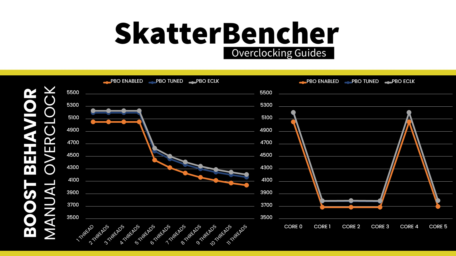
The Ryzen 5 8500GE boost frequency at 1 active thread is about 5050 MHZ and stays there when up to 4 C-core threads are active. When D-cores become active, the average boost frequency gradually trails off to 4036 MHz when all cores are active. The two C-cores can boost to 5050 MHz and the four D-cores can boost to 3.7 GHz in single-threaded workloads.

OC Strategy #2: PBO Tuned
In our second overclocking strategy, we tune the CPU’s Precision Boost dynamic frequency technology using the Precision Boost Overdrive 2 toolkit and optimize the memory subsystem performance.
PBO 2: Fmax Boost Override
Fused maximum frequency, or Fmax, is one of the Precision Boost infrastructure limiters constraining the CPU performance. The limiter determines the maximum allowed processor frequency across all CPU cores inside your Ryzen 5 8500GE.
Boost Clock Override or Fmax Override is one of the overclocker tools available in the PBO 2 toolkit. It allows the user to override the arbitrary clock frequency limit between -1000 MHz and +200 MHz in steps of 25 MHz. It’s important to note that the Fmax override only adjusts the upper ceiling of the frequency and doesn’t act as a frequency offset. Ultimately, the Precision Boost 2 algorithm still determines the actual operating frequency.
For most Ryzen processors, the Fmax Boost Override doesn’t need much further explanation. However, due to the unique Phoenix 2 architecture of this Ryzen 5 8500GE, we need to delve a little deeper.
As I mentioned at the beginning of the video, the C-cores and D-cores are functionally nearly identical other than the D-cores running a much lower frequency. The two types of cores are part of the same core complex (or “CCX”), so we’d expect they would run at the same frequency. However, that’s not the case.
For each of the two core types, there’s a 1T and nT maximum boost frequency.

The Ryzen 5 8500GE default 1T maximum boost frequency is 5050 MHz for the C-cores and 3700 MHz for the D-cores. When configuring the Fmax boost override, the 1T Fmax increases linearly. So, for example, if we set +150 MHz boost override, the new 1T max frequency is 5200 MHz for the C-cores and 3850 MHz for the D-cores.
The Ryzen 5 8500GE default nT maximum boost frequency is 4625 MHz for the C-cores and 3700 MHz for the D-cores. Configuring the Fmax boost override adjusts this frequency ceiling, but not linearly. For example, if we set +150 MHz boost override, the new nT max frequency is 4775 MHz for the C-cores and 3820 MHz for the D-cores. That’s respectively 125 and 120 MHz higher than stock.
For your reference, I plotted the Ryzen 5 8500GE 1T and nT Fmax for the C-cores and D-cores. We’ll discuss this graph in greater detail in our next overclocking strategy.

PBO 2: Curve Optimizer
Curve Optimizer is an important new feature of Precision Boost Overdrive 2.
Curve Optimizer allows end-users to adjust the factory-fused VFT or voltage-frequency-temperature curve for each CPU core separately. The VFT curve is a unique curve for each core inside your CPU that defines the required voltage for a given frequency at a given temperature. Higher frequencies or higher operating temperatures require higher voltage.
Curve Optimizer adjusts the VFT curve by offsetting the voltages of the factory-fused VFT curve. By setting a positive offset, you increase the voltage point. Conversely, you decrease the voltage point by setting a negative offset. You can offset the entire curve by up to 60 steps in a positive or negative direction. Each step represents approximately 5mV.

The traditional overclocking approach for AMD Ryzen CPUs is to set a negative curve optimizer. Two things happen when you adjust the VFT curve with a negative point offset.
- First, we effectively undervolt the CPU and tell it needs less voltage for a given frequency. And, as a consequence, at a given voltage, it can apply a higher frequency.
- Second, the CPU temperature will be lower because you use less voltage at a given frequency. That extra thermal headroom will also encourage the Precision Boost algorithm to target higher voltages and frequencies.
Like in the past, per-core tuning offers a real benefit as it provides some cores with a lot more frequency headroom. There’s no practical difference in the Curve Optimization process for the C-cores and D-cores.
Curve Optimizer Tuning Process
The manual tuning process for Curve Optimizer can become quite convoluted since it affects the CPU core voltage in all scenarios ranging from very light single-threaded workloads to heavy all-core workloads.
Usually, I spend a lot of time on per-core curve optimization. For this guide, I wanted to rely on the OCCT toolkit to find the right Curve Optimizer settings. Here’s my broad approach.
- I started with a negative curve optimizer of -15 for each core.
- Then, I used the OCCT CPU Stability test with small data set, extreme mode, and steady load type. I corecycle through each core for 60 seconds with 2 operating threads and AVX2.
- I increased the negative curve optimizer magnitude by 5 steps for the cores that didn’t crash.
- I reduced the negative curve optimizer magnitude by 5 steps for the cores that did crash.
- Once all cores were dialed in, I ran another OCCT AVX2 and SSE stability test intending to pass for 30 minutes without any core failing or clock stretching. Again, when a core fails, I reduce the negative curve optimizer magnitude by 5 steps.
Once all that’s done, I run through the usual benchmark suite and stability tests used in this guide. If there are no instabilities I consider my Curve Optimizer settings as stable.

Memory Subsystem Performance Optimization
On AMD Hawk Point processors, the memory subsystem consists of three major parts: the infinity fabric, the unified memory controller, and the system memory. They’re more commonly referred to as the FCLK, UCLK, and MCLK. First-generation Ryzen overclockers know that these parts used to be tightly coupled together, but on modern Ryzen processors like the Ryzen 5 8500GE, we can tune them independently.
There are two things I wanted to address with the memory subsystem optimization.
- First, I wanted to fix the downclocking of the FCLK and UCLK.
- Second, I wanted to run the UCLK and MCLK in sync
To solve the first problem, we simply enable SoC/Uncore OC mode in the AMD Overclocking submenu. This disables all power-saving technologies affecting the clock frequencies of the memory subsystem.
To address the second problem, we simply set UCLK DIV1 Mode to UCLK=MEMCLK. The memory controller frequency is tied directly to the system memory frequency. It can run either at the same or half its frequency.
You’d usually prefer to run the memory controller and system memory at the same frequency for performance reasons. However, if your memory can run very high frequencies, then it’s possible running the memory controller at half the frequency still provides better performance.
We run the memory controller frequency in sync with the system memory for this OC Strategy. At DDR5-6400, the memory controller frequency is then 3200 MHz.
ASUS EXPO Tweaked
EXPO Tweaked is an option available under Ai Overclock Tuner in addition to EXPO I and EXPO II. All three settings load the memory kit EXPO profile but do it slightly differently.
- EXPO I loads only the primary timings, frequency, and voltage. The secondary timings are adjusted by the motherboard auto-rules.
- EXPO II loads the complete EXPO profile, including the primary and secondary timings, the memory frequency, and the voltage.
- EXPO Tweaked loads the complete EXPO profile and adjusts various timings if possible.
Since memory performance may impact our benchmark performance, I tried the EXPO Tweaked setting. Everything seemed stable, so I used it for this OC Strategy.
BIOS Settings & Benchmark Results
Upon entering the BIOS
- Go to the Extreme Tweaker menu
- Set Ai Overclock Tuner to EXPO Tweaked
- Switch to Advanced menu
- Enter the AMD Overclocking submenu and click accept
- Enter the DDR and Infinity Fabric Frequency/Timings submenu
- Enter the Infinity Fabric Frequency and Dividers submenu
- Set UCLK DIV1 Mode to UCLK=MEMCLK
- Leave the Infinity Fabric Frequency and Dividers submenu
- Enter the Infinity Fabric Frequency and Dividers submenu
- Leave the DDR and Infinity Fabric Frequency/Timings submenu
- Enter the Precision Boost Overdrive submenu
- Set Precision Boost Overdrive to Advanced
- Set PBO Limits to Motherboard
- Set CPU Boost Clock Override to Enabled (Positive)
- Set Max CPU Boost Clock Override to 150
- Enter the Curve Optimizer submenu
- Set Curve Optimizer to Per Core
- For every Core, set Curve Optimizer Sign to Negative
- Set Core 0 Curve Optimizer Magnitude to 0
- Set Core 1, 2, 3, and 5 Curve Optimizer Magnitude to 25
- Set Core 4 Curve Optimizer Magnitude to 20
- Leave the Curve Optimizer submenu
- Leave the Precision Boost Overdrive submenu
- Enter the SoC/Uncore OC Mode submenu
- Set SoC/Uncore OC Mode to Enabled
- Enter the DDR and Infinity Fabric Frequency/Timings submenu
Then save and exit the BIOS.
We re-ran the benchmarks and checked the performance increase compared to the default operation.
- SuperPI 4M: +1.88%
- PYPrime 32B: +16.13%
- 7-Zip: 9.32%
- Geekbench 6 (single): +6.17%
- Geekbench 6 (multi): +9.02%
- Cinebench R23 Single: +9.62%
- Cinebench R23 Multi: +14.06%
- CPU-Z V17.01.64 Single: +4,59%
- CPU-Z V17.01.64 Multi: +4.52%
- V-Ray 5: +12.68%
- Corona 10: +13.17%
- AI Benchmark: +9.16%
- Y-Cruncher Pi 5B: +8.18%
- 3DMark Night Raid: +10.94%
- Returnal: +1.89%
- Tomb Raider: +7.69%
- Final Fantasy XV: +6.72%

Here are the 3DMark CPU Profile scores:
- CPU Profile 1 Thread: +3.46%
- CPU Profile 2 Threads: +7.02%
- CPU Profile 4 Threads: +6.06%
- CPU Profile 8 Threads: +6.00%
- CPU Profile 16 Threads: +5.87%
- CPU Profile Max Threads: +5.86%

While we aren’t able to maximize the Fmax Boost Override overclock due to C-core headroom, we can undervolt the D-cores significantly using Curve Optimizer. This yields a nice performance uplift in both single-threaded and multi-threaded workloads. The Geomean performance improvement is +6.87%, and we get a maximum improvement of +16.13% in PYPrime 32B.

When running the OCCT CPU AVX2 Stability Test, the average CPU C-core effective clock is 4748 MHz and the average CPU D-core effective clock is 3799 MHz. The average CPU core voltage is 1.199 volts. The average CPU temperature is 74.3 degrees Celsius. The average CPU package power is 84.9 watts.

When running the OCCT CPU SSE Stability Test, the average CPU C-core effective clock is 4752 MHz and the average CPU D-core effective clock is 3802 MHz. The average CPU core voltage is 1.199 volts. The average CPU temperature is 68.3 degrees Celsius. The average CPU package power is 71.5 watts.

The boost frequency at 1 active thread is 5200 MHZ and stays there when up to 4 C-core threads are active. When D-cores become active, the average boost frequency gradually trails off to 4167 MHz when all cores are active. The two C-cores can boost to 5200 MHz and the four D-cores can boost to nearly 3.8 GHz in single-threaded workloads.

OC Strategy #3: PBO Asynchronous Eclk
In our third overclocking strategy, we take advantage of the return of the ECLK mode.
ECLK stands for external clock and is precisely what the term suggests: an external clock generator. It was previously available on Ryzen 2000 Pinnacle Ridge processors but was removed afterward. I’ve used ECLK for many Ryzen 7000 series overclocking strategies as it allows us to go beyond the Precision Boost frequency limit. However, it’s the first time I’m using Eclk with a Hawk Point APU.
As I mentioned a couple of times, the Phoenix 2 architecture is unusual with the two types of compute cores. So before we talk about Eclk, let’s first have a look at the Phoenix 2 frequency and voltage topology.
AMD Phoenix 2 Clocking Topology
The clocking of Phoenix is similar to other AMD Zen 4 CPUs.

The standard Phoenix 2 APU has a 48 MHz crystal input to the integrated CGPLL clock generator. The CGPLL then generates a 48 MHz clock for the USB PLL and a 100 MHz reference clock for the FCH, which contains the CCLK PLL for the CPU cores and several SOC PLLs.
The CCLK PLL 100MHz reference clock drives the 200 MHz VCO, which is then multiplied by a frequency ID (FID) and divided by a divider ID (DID). As a whole, this provides a core clock frequency granularity of 25 MHz. Each CCX has its own PLL, with the cores within that CCX running at the same frequency.
For Phoenix 2, the C-cores and D-cores are part of the same CCX. However, the D-cores operate at a significantly lower frequency. This is counter-intuitive as we always learned that the cores inside the CCX operate the same clock. I’ll get back to this in a minute.
The SOC PLLs include a wide range of PLLs. The ones most relevant for overclocking are:
- FCLK for the data fabric
- UCLK for the memory controller
- MCLK for the system memory
- GFXCLK for the integrated graphics
The SOC PLLs are not particularly relevant for manual CPU Core overclocking.
Just like on Ryzen 7000 Raphael CPUs, the Ryzen 8000 Phoenix 2 processors support Asynchronous Eclk. ECLK stands for external clock and is exactly what the term suggests: external clock generator inputs. The external clocks are inputs to the FCH. There you can configure how you want to use the external clocks. In addition to the standard internal CGPLL, Phoenix 2 supports up to two external clock modes. They’re called eCLK0 Mode and eCLK1 Mode.
- In eCLK0 Mode, an external 100MHz reference clock is used for both the CPU and SOC PLLs. In other words, it’s a reference clock that affects the CPU core clocks and the PCIe and SATA clocks.
- In eCLK1 Mode, there are two distinct external 100MHz reference clocks. One clock provides the 100MHz input for the Core PLL, and another provides the 100MHz reference clock for the SOC PLLs.


The overclocking strategy with ECLK is the polar opposite of what we’re used to with Ryzen CPUs. OC Strategy #2 shows that Ryzen overclocking is typically done with a negative curve optimizer. That pushes the Precision Boost algorithm to reach higher boost frequencies.
With ECLK, we still build on the factory-fused VFT curve but adjust the frequency by adjusting the reference clock. For example, if the Precision Boost has a VFT point for 4500 MHz at 1.0V at 50C, with an ECLK of 105 MHz, the actual point will be 4725 MHz at 1.0V at 50C.
C-core and D-core Multipliers
I already mentioned it a couple of times: the Phoenix 2 CPU core clocking is a little odd due to the mixed core types. Let’s have a closer look at what’s going on. We can distinguish two scenarios: when either C- or D-cores are active, or when they’re both active.
In the scenario where either C- or D-cores are active (doesn’t matter how many), the behavior is pretty simple: each core type can boost to its programmed Fmax. At stock, that’s 5050 MHz for the C-cores and 3700 MHz for the D-cores.

In the scenario where both C- and D-cores are active, the behavior is a little more complex as the C- and D-cores will operate at a fixed relative ratio. At stock, the C-core operates at 1.25X the frequency of the D-core. This ratio is 1.50X when we set a Fmax boost override of -300 MHz or lower.

As I mentioned, that’s a little odd as we always learned that all cores inside a CCX should operate at the same frequency. However, that’s only partially true. The way it seems to work is that the reference clock and FID are the same for all cores within the CCX, however the DID can be different per core. Let’s look at an example:
Let’s say the reference clock (VCO) is 200 MHz, the FID is 185, and the DID is 8. In that case, the operating frequency is 200 x 185 / 8 = 4625 MHz. By using a DID of 10 for the D-cores, the frequency becomes 200 x 185 / 10 = 3700 MHz. Incidentally, this is the default frequency for the Ryzen 5 8500GE.
Let’s say we increase the frequency by configuring a Fmax Boost Override of +200 MHz. In that case, the nT Fmax limit for the C-cores is 4775 MHz. This can be set with an FID of 191 (200 x 191 / 8 = 4775 MHz). With the D-cores using a DID of 10, their frequency is then 200 x 191 / 10 = 3820 MHz. We can confirm this frequency when checking the operating clocks in Windows with HWiNFO.
This also holds true when the C-to-D-core nT ratio is 1.50X. For example, let’s say we set the Fmax Boost Override to -400 MHz. In that case, the nT Fmax limit for the C-cores is 4650 MHz. This can be set with an FID of 186 (200 x 186 / 8 = 4650 MHz). With the D-cores now using a DID of 12 (to get the 1.50X ratio), their frequency is then 200 x 186 / 12 = 3100 MHz. We can confirm this frequency when checking the operating clocks in Windows with HWiNFO.

As a final note to this topic: the difference in DID also adds further granularity to the operating clock frequency. We’re used to Ryzen having a granularity of 25 MHz frequency, but that’s not the case with Phoenix 2. If we set the Fmax to -375 MHz, for example, the nT frequency for the D-core is 3116 MHz. That’s a frequency granularity is 16.67 MHz. Assuming the DID is a 1-bit hex value (0 to F), perhaps Ryzen supports ratio granularity up to 12.5 MHz.

Anyway, now that we know everything about the Phoenix 2 clocking, let’s have a look at the voltage topology.
AMD Phoenix 2 Voltage Topology
AMD Phoenix 2 voltage topology is similar to that of previous Ryzen processors but with two significant differences.

As usual, the processor relies on an internal and external power supply to generate the processor voltages. There are four primary power supplies from the motherboard VRM to the processor: VDDCR, VDDCR_SOC, VDDCR_MISC, and VDDIO_MEM.
The VDDCR voltage rail provides the external power for three internal voltage regulators: VDDCR_CPU, VDDCR_VDDM, and the VDDCR_GFX.
VDDCR_CPU provides the voltage for the CPU cores within the CCX. The voltage rail can work in either regular or bypass mode, but it is always in bypass mode on Phoenix 2. That means the voltage of the cores is always equal to the VDDCR external voltage.
Since the D-cores have a much higher transistor density, they can’t handle too much voltage. Therefore, AMD has implemented a voltage limit of 1.2V. In practical terms, the external VDDCR voltage rail is regulated to 1.2V when a D-core is active. This also limits the voltage supplied to the C-cores and therefore will restrict its operating frequency. When all D-cores are power-gated (in sleep mode), then the external VDDCR voltage rail can provide a higher voltage to the C-cores to support its higher frequency capabilities.
Due to this voltage limitation requirement, unfortunately, the end user cannot change the voltage in the BIOS.
VDDCR_VDDM provides the voltage for the L2, L3, and, if present, 3D V-Cache on a CCX. This rail cannot work in bypass mode; therefore, it is always internally regulated from the VDDCR external voltage rail. We can also not adjust this voltage.
VDDCR_GFX provides the voltage for the integrated graphics. In the past, this voltage would be provided by the VDDCR_SOC voltage rail. Still, it’s likely due to the high current requirements of the powerful integrated graphics, using the typically beefier VDDCR voltage plane is safer. The voltage rail can technically work in regular or bypass mode, but only regular mode is available. In regular mode, the voltage is managed by the integrated voltage regulator and derived from the VDDCR voltage rail. This voltage is limited to 1.20V on Phoenix 2.
The VDDCR_SOC voltage rail provides the external power for multiple internal voltage regulators on SOC for the various IP blocks, including but not limited to the memory controller, SMU, PSP, etc. It is essential to know that the VDDCR_SOC voltage must always be lower than VDDIO_MEM_S3 + 100mV. The default VDDCR_SOC voltage is 1.05V and can be set to 1.30V under ambient conditions.
The VDDCR_MISC voltage rail provides the external power for the internally regulated VDDG voltage rail. VDDG is the voltage supply for the infinity fabric data path. On designs with multiple chiplets which require physical GMI links to communicate, there are VDDG voltage tuning options in the BIOS. Since Phoenix 2 is a monolithic chip design, it doesn’t have these tuning options despite, obviously, still using infinity fabric to communicate between the various IP blocks in the die.
The VDDIO_MEM voltage rail provides the external power for the VDDP_DDR internal voltage regulator. VDDP is the voltage for the DDR bus signaling or DRAM PHY. So, it can help achieve higher memory frequencies. As a rule, the external VDDIO_MEM should always be higher than the internal VDDP_DDR + 100mV. Furthermore, the external VDDCR_SOC voltage rail should be lower than the external VDDIO_MEM + 100mV. When memory overclocking, you may need to manually increase the VDDP voltage as it does not automatically adjust when changing the VDDIO_MEM voltage.
ECLK Tuning Process
The ECLK tuning process for Phoenix 2 is extraordinarily complex due to the mixed CPU core types and multiple Fmax limiters. Furthermore, the Fmax Boost Override knob doesn’t work as we’d expect for increasing the nT frequency as I illustrated earlier in the video.
For this OC Strategy, my goal was to maximize the frequency for multi-threaded workloads. The key limiting factor is the C-core 1T frequency which becomes unstable around 5.2 GHz. The trick is to find the Fmax Boost Override setting which minimizes the frequency delta between the C-cores and D-cores. In the case of the Ryzen 5 8500GE, that’s at +100 and +125 MHz boost override.

For these two settings, the delta between:
- 1T C-core and D-core is 400 MHz,
- 1T and nT C-core is 1350 MHz, and
- 1T and nT C-core is 950/955 MHz.
By minimizing the frequency delta, we can increase the D-core frequency the most until the C-core becomes unstable.
The testing process is similar to that we used for finding the best Curve Optimizer settings, with one major caveat: we can also use a positive curve optimizer setting to, effectively, overvolt specific cores that become unstable. This was necessary, especially for Core 0.
I found that the maximum stable overclock was with 101 MHz ECLK frequency which, combined with an Fmax boost override of +125 MHz, yields 1T C-core and D-core frequencies of 5227 and 3863 MHz and nT frequencies of 4823 and 3858 MHz.

Memory Subsystem Performance Optimization (2)
In addition to the core overclocking, I also made a couple of minor adjustments to the memory subsystem performance by increasing the FCLK to 2600 MHz and the MCLK to DDR5-6600. Since we have the UCLK run in sync with the MCLK, it also increases slightly to 3.3 GHz.
BIOS Settings & Benchmark Results
Upon entering the BIOS
- Go to the Extreme Tweaker menu
- Set Ai Overclock Tuner to EXPO Tweaked
- Set eCLK Mode to Asynchronous Mode
- Set BCLK2 Frequency to 101
- Set Memory Frequency to DDR5-6600MHz
- Switch to Advanced menu
- Enter the AMD Overclocking submenu and click accept
- Enter the DDR and Infinity Fabric Frequency/Timings submenu
- Enter the Infinity Fabric Frequency and Dividers submenu
- Set Infinity Fabric Frequency and Dividers to 2600 MHz
- Set UCLK DIV1 Mode to UCLK=MEMCLK
- Leave the Infinity Fabric Frequency and Dividers submenu
- Enter the Infinity Fabric Frequency and Dividers submenu
- Leave the DDR and Infinity Fabric Frequency/Timings submenu
- Enter the Precision Boost Overdrive submenu
- Set Precision Boost Overdrive to Advanced
- Set PBO Limits to Motherboard
- Set CPU Boost Clock Override to Enabled (Positive)
- Set Max CPU Boost Clock Override to 125
- Enter the Curve Optimizer submenu
- Set Curve Optimizer to Per Core
- Set Core 0 Curve Optimizer Sign to Positive
- Set Core 0 Curve Optimizer Magnitude to 15
- Set Core 1, 2, 3, 4, and 5 Curve Optimizer Sign to Negative
- Set Core 1 Curve Optimizer Magnitude to 20
- Set Core 2, 3, and 5 Curve Optimizer Magnitude to 25
- Set Core 4 Curve Optimizer Magnitude to 5
- Set Curve Optimizer to Per Core
- Leave the Curve Optimizer submenu
- Leave the Precision Boost Overdrive submenu
- Enter the SoC/Uncore OC Mode submenu
- Set SoC/Uncore OC Mode to Enabled
- Enter the DDR and Infinity Fabric Frequency/Timings submenu
Then save and exit the BIOS.
We re-ran the benchmarks and checked the performance increase compared to the default operation.
- SuperPI 4M: +3.02%
- PYPrime 32B: +17.83%
- 7-Zip: +10.73%
- Geekbench 6 (single): +6.70%
- Geekbench 6 (multi): +10.34%
- Cinebench R23 Single: +10.58%
- Cinebench R23 Multi: +15.48%
- CPU-Z V17.01.64 Single: +5.15%
- CPU-Z V17.01.64 Multi: +5.54%
- V-Ray 5: +13.52%
- Corona 10: +13.72%
- AI Benchmark: +10.45%
- Y-Cruncher Pi 5B: +11.69%
- 3DMark Night Raid: +12.08%
- Returnal: +1.89%
- Tomb Raider: +8.33%
- Final Fantasy XV: +6.83%

Here are the 3DMark CPU Profile scores:
- CPU Profile 1 Thread: +4.05%
- CPU Profile 2 Threads: +7.07%
- CPU Profile 4 Threads: +6.15%
- CPU Profile 8 Threads: +6.33%
- CPU Profile 16 Threads: +6.48%
- CPU Profile Max Threads: +7.16%

We have to do a lot of finetuning to push the CPU core frequency up marginally. That translates into a small but noticeable improvement in performance across single-threaded and multi-threaded workloads. The Geomean performance improvement is +7.75%, and we get a maximum improvement of +17.83% in PYPrime 32B.

When running the OCCT CPU AVX2 Stability Test, the average CPU C-core effective clock is 4776 MHz and the average CPU D-core effective clock is 3820 MHz. The average CPU core voltage is 1.191 volts. The average CPU temperature is 75.0 degrees Celsius. The average CPU package power is 75.0 watts.

When running the OCCT CPU SSE Stability Test, the average CPU C-core effective clock is 4797 MHz and the average CPU D-core effective clock is 3838 MHz. The average CPU core voltage is 1.199 volts. The average CPU temperature is 68.4 degrees Celsius. The average CPU package power is 72.0 watts.

The boost frequency at 1 active thread is 5227 MHZ and stays there when up to 4 C-core threads are active. When D-cores become active, the average boost frequency gradually trails off to 4209 MHz when all cores are active. The two C-cores can boost to slightly over 5.2 GHz and the four D-cores can boost to nearly 3.8 GHz in single-threaded workloads.
AMD Ryzen 5 8500GE: Conclusion
Alright, let us wrap this up.
I was very excited to try overclocking the Phoenix 2 architecture because it’s such an unusual design with two Zen 4 and four Zen 4c cores. We should refer to those as the C-cores and D-cores according to AMD nomenclature, though it gets a bit confusing since the C-cores are not actually Zen 4c.
I don’t have too much to say about the performance improvement from overclocking. It’s a very similar experience to the other Ryzen 8000 APUs I overclocked before. At the end of the day, the C-cores are pretty limited in overclocking headroom either due to the chip architecture or the manufacturing process. Ultimately, that’s the limiting factor for performance tuning.
The most interesting aspect of the Phoenix 2 chip is the clocking and voltage topology. It’s already a non-trivial setup with different Fmax limits for each core type in 1T and nT workloads, and the shared voltage rail and voltage limitation rules add further complexity. Overall, it’s quite a lot of work to truly maximize the CPU compute performance of Phoenix 2 APUs.
Anyway, that’s all for today! I’m also preparing an overclocking guide for this APU’s integrated graphics, so stay tuned if you’re interested in that. I want to thank my Patreon supporters for supporting my work. If you have any questions or comments, please drop them in the comment section below.
See you next time!