SkatterBencher #62: NVIDIA GeForce RTX 3050 Overclocked to 2220 MHz

We overclock the NVIDIA GeForce RTX 3050 up to 2200 MHz with the EVGA XC Gaming graphics card and custom loop water cooling.
The RTX 3050 is the third NVIDIA graphics card I tried since returning to discrete graphics card overclocking last year. I usually try the most low-end versions of an architecture because they’re cheaper to play with. I previously overclocked the GT 1030 and GTX 1650.
This article took me a very long time to finish, and it’s one of the most frustrating yet edifying projects I’ve undertaken on this blog. I apologize for the post length in advance and hope you enjoy the read. Let’s jump in!
NVIDIA GeForce RTX 3050: Introduction
The NVIDIA GeForce RTX 3050 is the slowest graphics card in NVIDIA’s Ampere desktop GPU lineup. NVIDIA released the original RTX 3050 with GA106 die on January 27, 2022, about one year and a half after the release of its bigger brother, the RTX 3090. Since that release, two additional variants entered the market: one OEM exclusive with slightly fewer CUDA cores and one based on the GA107 die.
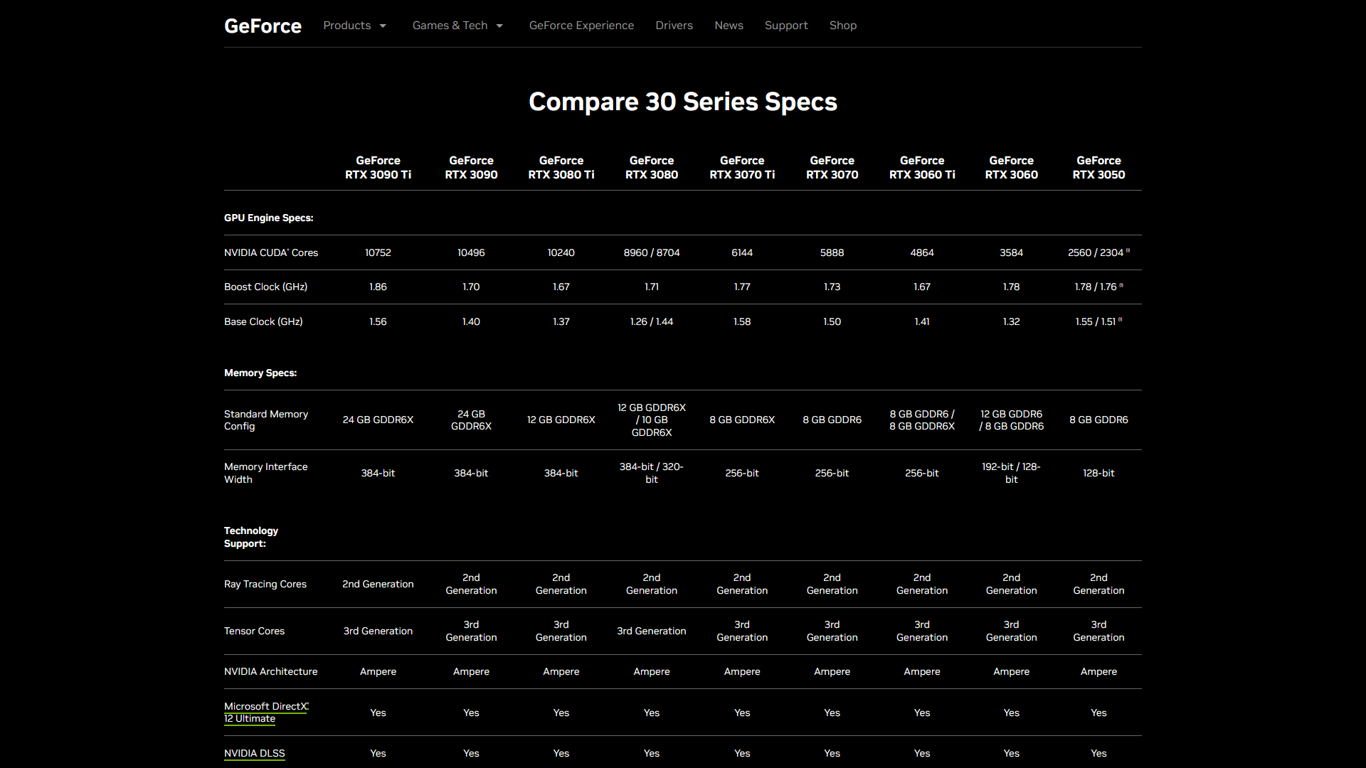
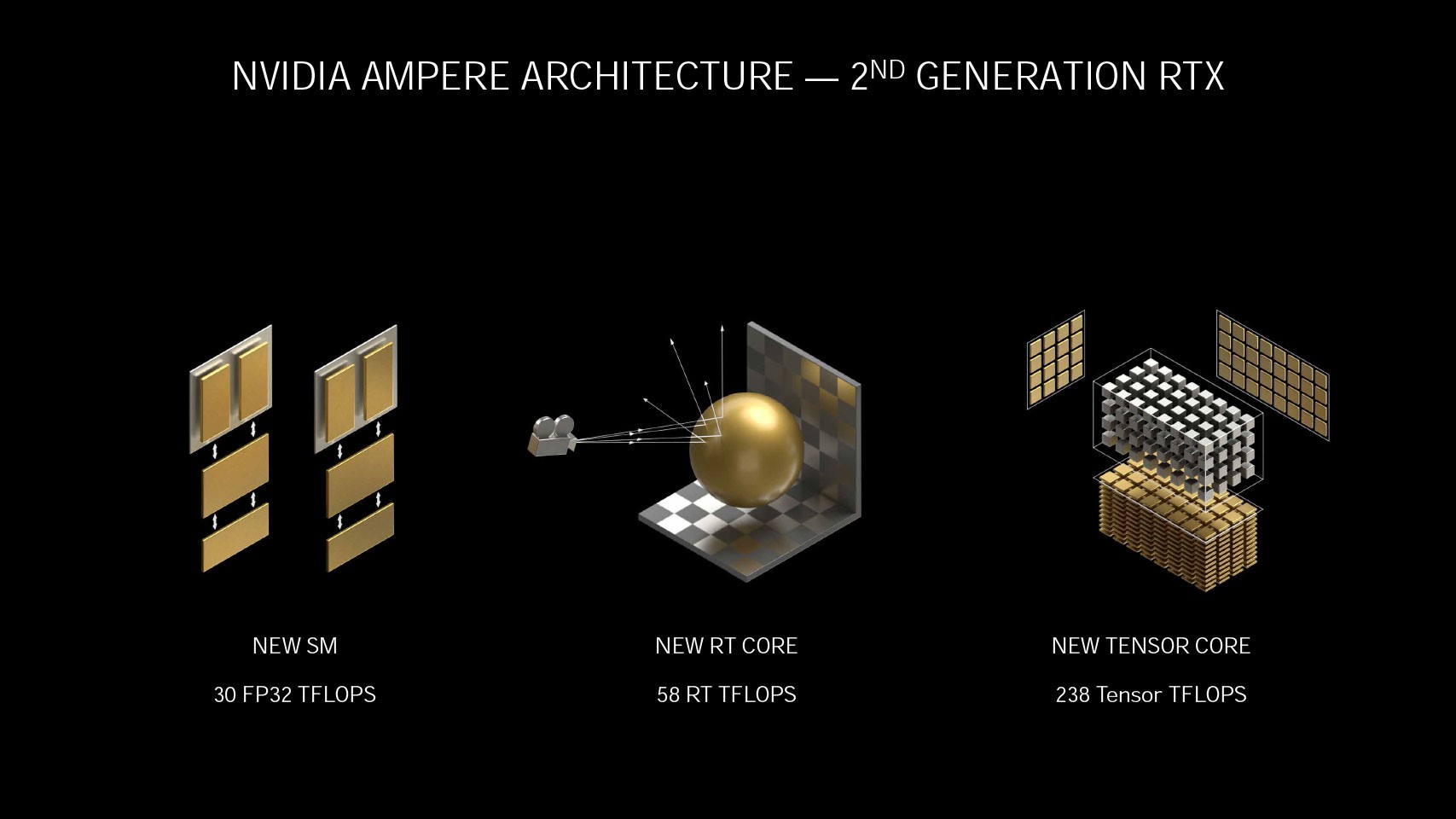
The GeForce 30 series launch was hectic. It launched when COVID-19 caused turbulence in the PC market. But let’s not get into that topic. What’s important to know about the RTX 30 series and the Ampere architecture is that it features 2nd gen ray tracing (RT) cores and 3rd gen Tensor Cores.

The GeForce RTX 3050 with 8 GB GDDR6 is built on the Samsung 8nm process and houses 2560 CUDA Cores, 80 tensor cores, and 20 RT cores. It has a base clock of 1552 MHz and a boost clock of 1777 MHz. The memory clocks in at 1750 MHz. The graphics card power is limited to 130W.
In today’s video, we tackle overclocking the GeForce RTX 3050. We will cover three overclocking strategies.
- We manually increase the GPU and memory frequency with the EVGA Precision X1 software tool.
- We slap on a full-cover water block and try to overcome the power limitations by shunt modding.
- We use the ElmorLabs EVC2 to work around other overclocking limitations.

Before jumping into the overclocking, let us quickly review the hardware and benchmarks used in this video.
NVIDIA GeForce RTX 3050: Platform Overview
The system we’re overclocking today consists of the following hardware.
| Item | SKU | Price (USD) |
| CPU | Intel Core i9-13900K | 540 |
| Motherboard | ASUS ROG Maximus Z790 Hero | 582 |
| CPU Cooling | Noctua NH-L9i-17xx Chromax.black | 55 |
| GPU Cooling | Bykski N-EV3060XC-X EK-KIT P360 | 190 |
| Fan Controller | ElmorLabs EFC | 20 |
| Memory | G.SKILL Trident Z DDR5-7800 CL36 32GB | 200 |
| Power Supply | Enermax REVOLUTION ATX 3.0 1200W | 250 |
| Storage | Kingston SSDNow SV300S37A/120 (x2) | 50 |
| Chassis | Open Benchtable V2 | 200 |
EVGA GeForce RTX 3050 XC GAMING
The specific graphics card we’re using to overclock the RTX 3050 GPU is the EVGA GeForce RTX 3050 XC GAMING (08G-P5-3553-KR). Of course, unfortunately, EVGA has recently exited the GPU business.

The card has a dual fan thermal solution and an out-of-the-box listed GPU boost frequency of 1845 MHz, slightly up from NVIDIA’s 1777 MHz specification. However, it appears as if EVGA overclocked the GPU even further as we get up to 2055 MHz when we power up the card.
We’ll get back to that later in the video.
NVIDIA GeForce RTX 3050: Benchmark Software
We use Windows 11 and the following benchmark applications to measure performance and ensure system stability.
I’m introducing a couple of new benchmarks we haven’t used in previous SkatterBencher guides. So, let me quickly explain what they are and why I’m including them in this guide.
3DMark Speedway Stress Test
In all my overclocking guides, in addition to the performance benchmarks, I rely on worst-case workloads to assess the stability of a given overclock. For graphics devices such as discrete graphics cards, I’ve always relied on Furmark. While Furmark represents a worst-case scenario workload and usually puts up the highest power and lowest stable frequencies on the board, it’s not representative of a gaming scenario. So, I wanted to include a new stress test that’s a more reasonable proxy for a heavy gaming workload.
On June 13, 2016, UL introduced a new 3DMark Stress Test tool based on their benchmark workloads. Stress testing aims to place a high load on your system for an extended period to expose any problems with stability and reliability. It can also help identify faulty hardware or the need for better cooling. In 2022, 3DMark expanded its Stress Test function with Speedway, a DirectX 12 Ultimate workload. It’s that workload we’re using in this guide.
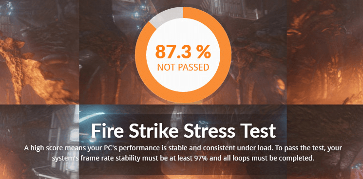
Each 3DMark Stress Test loops 20 times or about 10 minutes, which is usually enough to uncover any stability or cooling issues. After running a 3DMark Stress Test, you will see your system’s Frame Rate Stability score. A high score means your PC’s performance under load is stable and consistent. To pass the stability test, your system must complete all loops with a Frame Rate Stability of at least 97%.
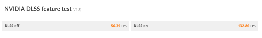
3DMark DLSS Feature Test
NVIDIA Deep Learning Super Sampling, or DLSS, is a key selling point of any GeForce RTX graphics card. In short, it’s a set of real-time deep-learning image enhancement and upscaling technologies. The goal is to allow most of the graphics pipeline to run at a lower resolution for increased performance and then infer a higher-resolution image that approximates the same level of detail as if the image was rendered at this higher resolution. The point is to output images at an equal quality but with lower power.

NVIDIA introduced the technology in February 2019. UL immediately announced it added the NVIDIA DLSS Feature Test to its 3DMark benchmark suite. Since AI-inferred image generation is an imported feature offered by NVIDIA GPUs, I figured including a performance benchmark is essential.
I use the 3DMark DLSS Feature Test and calculate the difference between “DLSS off” and “DLSS on” to measure how overclocking affects DLSS performance.
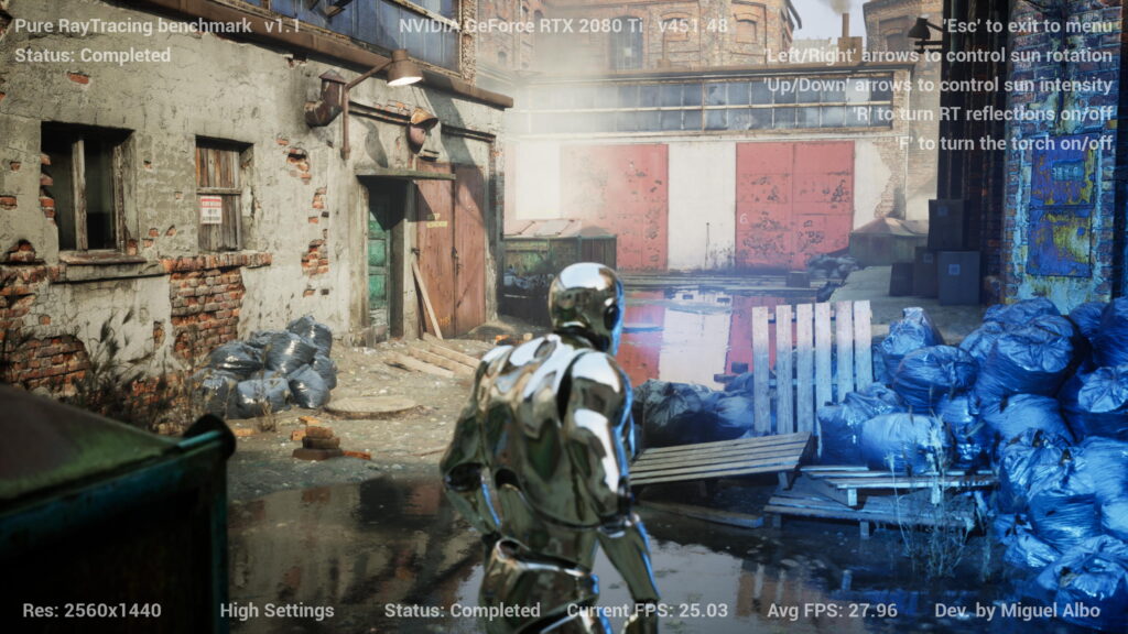
Pure Raytracing Benchmark
I already included the Simple Raytracing benchmark by MARvizer in previous SkatterBencher guides. When I saw he also has a Pure Raytracing benchmark, I figured I should add it too. I don’t have much else to add than that.
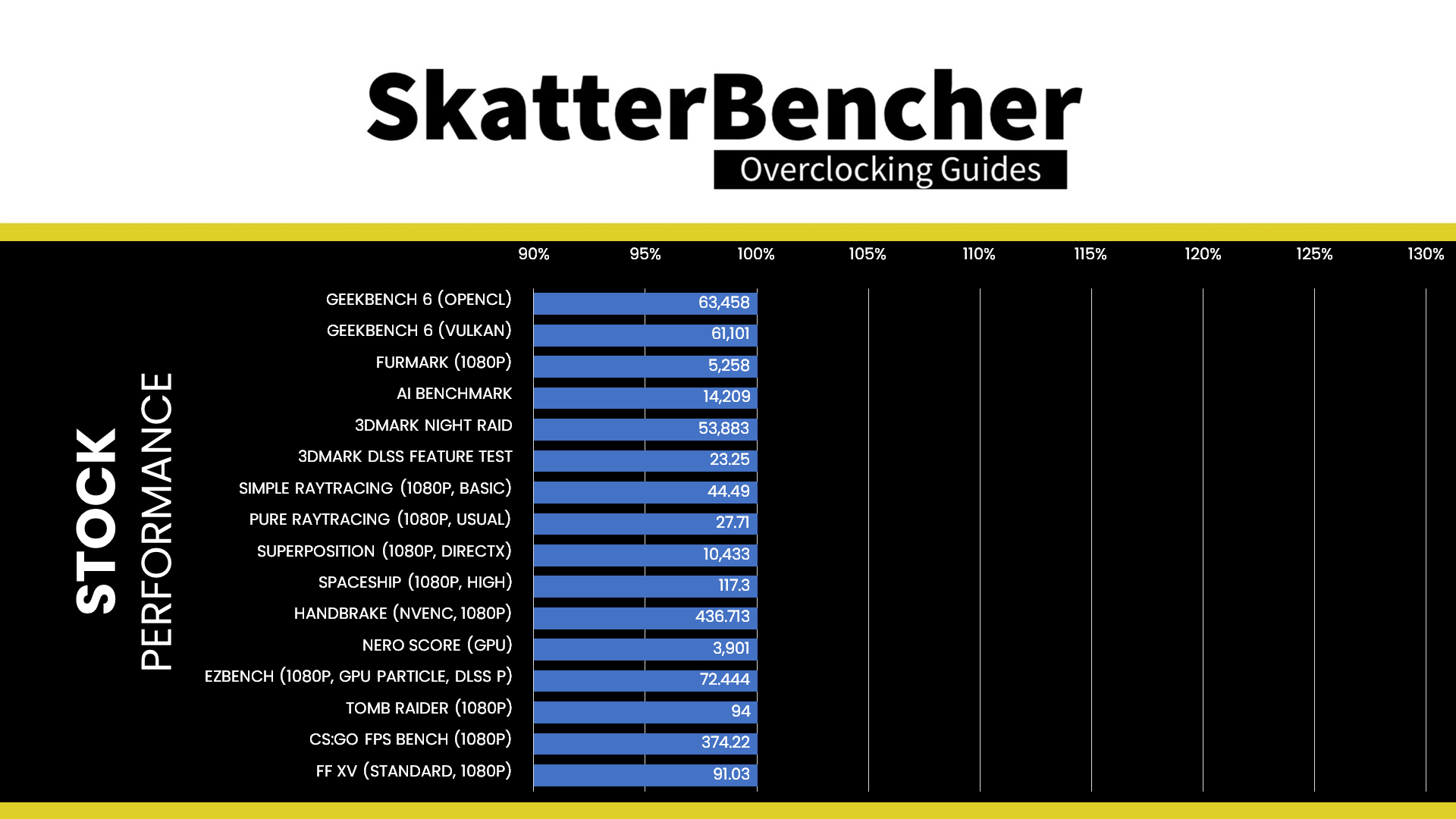
NVIDIA GeForce RTX 3050: Stock Performance
Before starting overclocking, we must check the system performance at default settings.
As I mentioned, the EVGA card we’re using in this guide has a listed (1845 MHz) and actual (2055 MHz) maximum boost clock that’s higher than NVIDIA’s listed (1777 MHz) specification. So, to get the stock performance of the RTX 3050, I manually adjust the maximum boost frequency back to 1777 MHz.
Here is the benchmark performance at stock:
- Geekbench 6 OpenCL: 63,458 points
- Geekbench 6 Vulkan: 61,101 points
- Furmark 1080P: 5,258 points
- AI Benchmark: 14,209 points
- 3DMark Night Raid: 53,883 marks
- 3DMark DLSS Feature Test: 23.25 fps
- Simple Raytracing: 44.49 fps
- Pure Raytracing: 27.71 fps
- Unigine Superposition: 10,433 points
- Spaceship: 117.3 fps
- Handbrake: 436.713 fps
- Nero Score: 3,901 points
- EZBench: 72.444 fps
- Shadow of the Tomb Raider: 94 fps
- CS:GO FPS Bench: 374.22 fps
- Final Fantasy XV: 91.03 fps
Then, we reset the card to its out-of-the-box clocks and re-ran the benchmarks to check the performance increase compared to the default operation.
- Geekbench 6 OpenCL: +9.06%
- Geekbench 6 Vulkan: +8.64%
- Furmark 1080P: +4.53%
- AI Benchmark: +2.44%
- 3DMark Night Raid: +0.79%
- 3DMark DLSS Feature Test: +10.41%
- Simple Raytracing: +10.07%
- Pure Raytracing: +15.08%
- Unigine Superposition: +10.90%
- Spaceship: +10.14%
- Handbrake: +0.04%
- Nero Score: +4.31%
- EZBench: +8.66%
- Shadow of the Tomb Raider: +9.57%
- CS:GO FPS Bench: +3.00%
- Final Fantasy XV: +10.74%
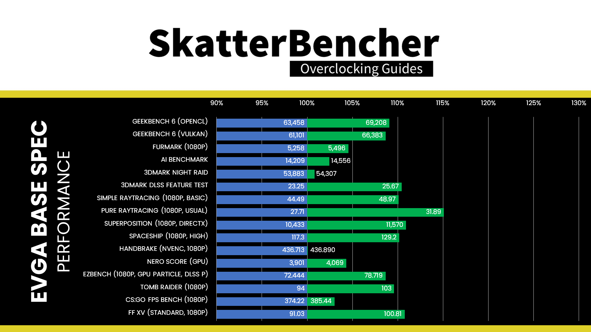
The out-of-the-box performance boost of this EVGA RTX 3050 graphics card is about 10% over NVIDIA’s listed specifications.
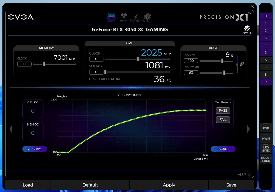
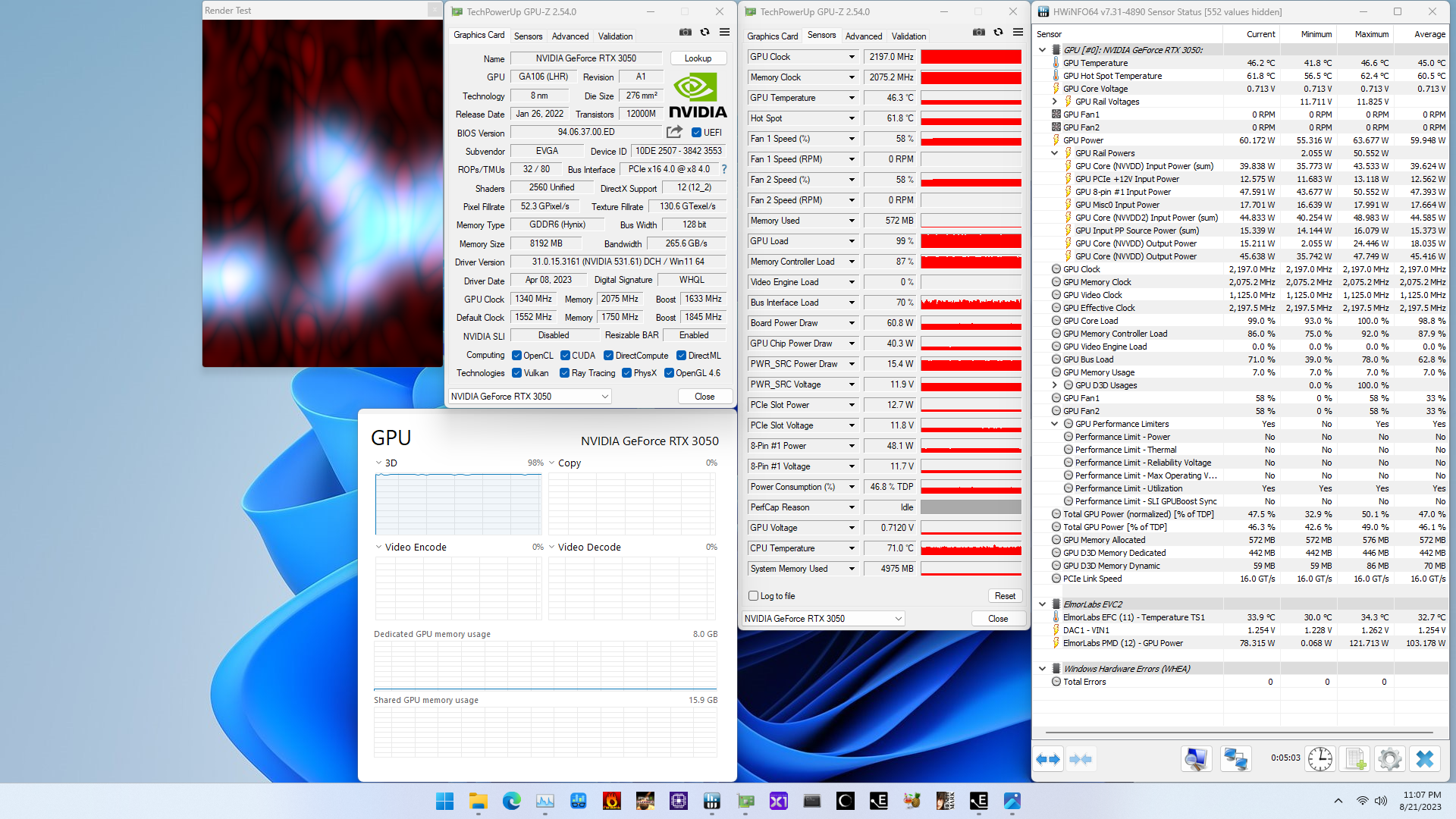
When running the GPU-Z Render Test, the maximum GPU Clock is 2032 MHz with 1.081V.
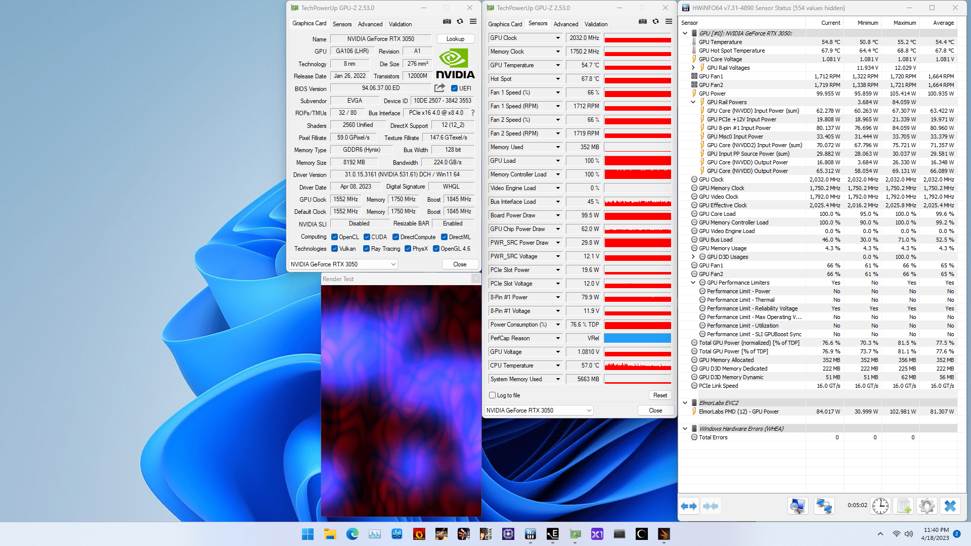
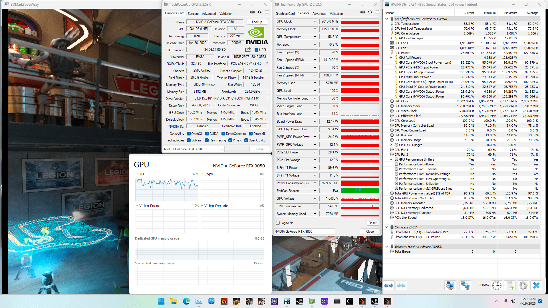
When running the 3DMark Speedway Stability Test, the average GPU effective clock is 1996 MHz with 1.066 volts, and the GPU Memory clock is 1750 MHz. The average GPU and GPU Hot Spot temperatures are 59.2 and 70.9 degrees Celsius. The average GPU power is 127.358 watts.
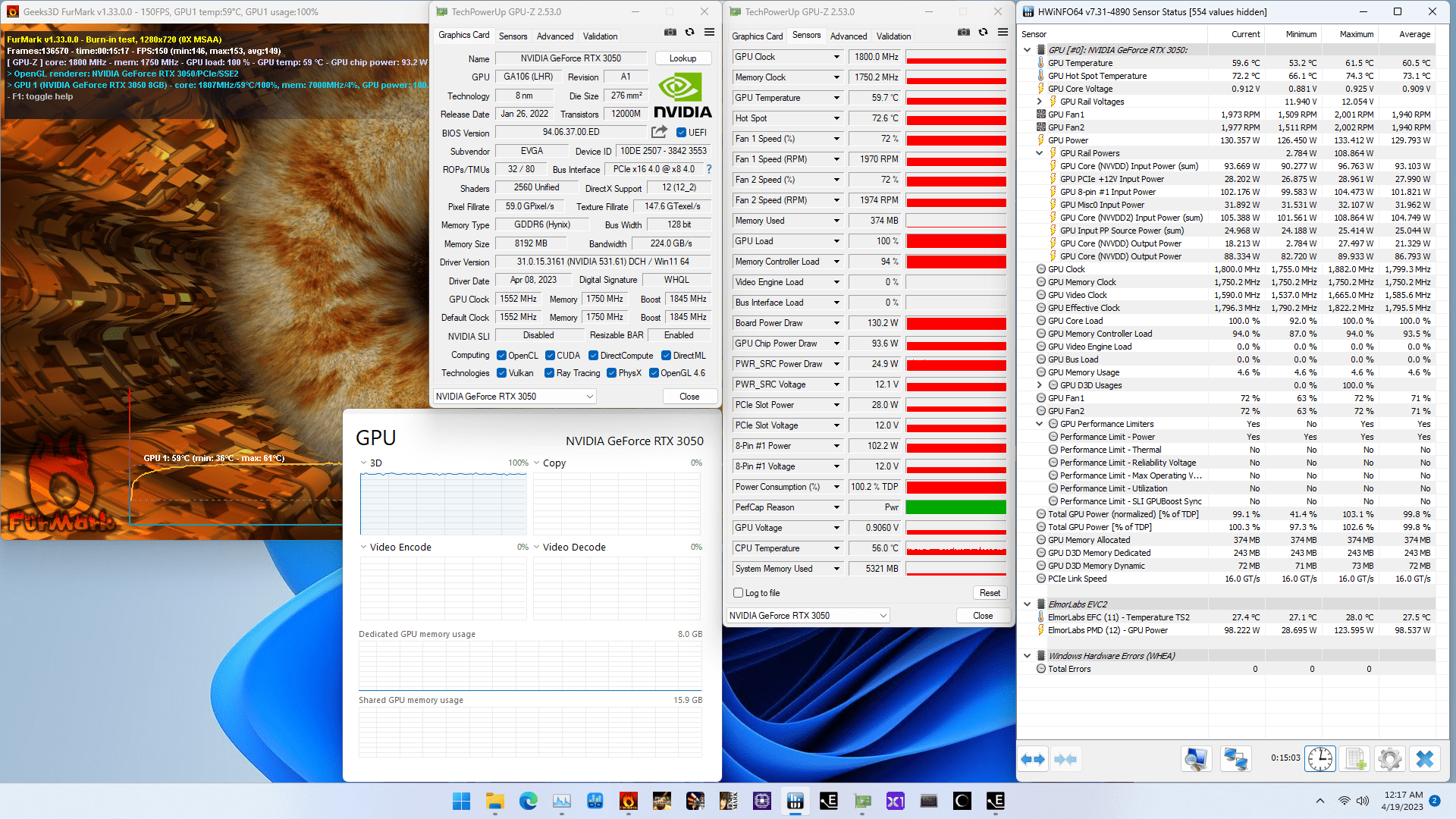
When running the Furmark GPU Stress Test, the average GPU effective clock is 1796 MHz with 0.909 volts, and the GPU Memory clock is 1750 MHz. The average GPU and GPU Hot Spot temperatures are 60.5 and 73.1 degrees Celsius. The average GPU power is 129.793 watts.
OC Strategy #1: EVGA Precision X1
In our first overclocking strategy, we rely on the overclocking toolkit integrated into the NVIDIA GPU Boost Technology and the EVGA Precision X1 software to overclock the GeForce RTX 3050 graphics card manually.
NVIDIA GPU Boost “5.0” Technology
NVIDIA didn’t provide much information on implementing the GPU Boost performance-maximizing technology on Ampere. W1zzard from TechpowerUP did a great job of explaining the intricate differences between Ampere and its predecessor, Turing.
Speaking of Turing, when it introduced the architecture on September 20, 2018, NVIDIA also introduced GPU Boost 4.0. The fourth iteration of GPU Boost Technology builds on the foundations laid since the introduction of GPU Boost Technology in 2012. I already have a couple pages up on this website detailing how GPU Boost works. So, I won’t go into too much detail this time. Instead, I will focus on the central aspect of the GPU Boost technology: its voltage-frequency curve.
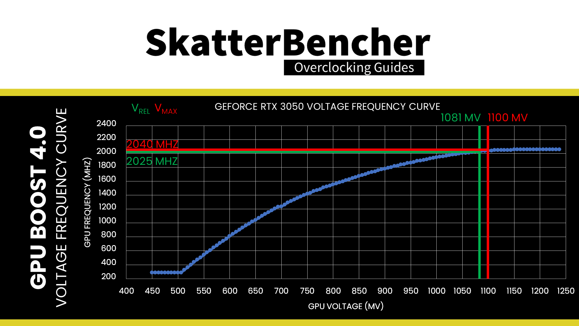
The voltage-frequency curve is precisely what the name says: it’s a curve that describes the relationship between a frequency and the voltage required to run that frequency. The NVIDIA Ampere GPU has 128 distinct, individually adjustable points on its voltage-frequency curve. With each step, the voltage increases by 6.25mV. On this RTX 3050, the V/F points range from 285 MHz at 450 mV to 2055 MHz at 1237.5 mV.
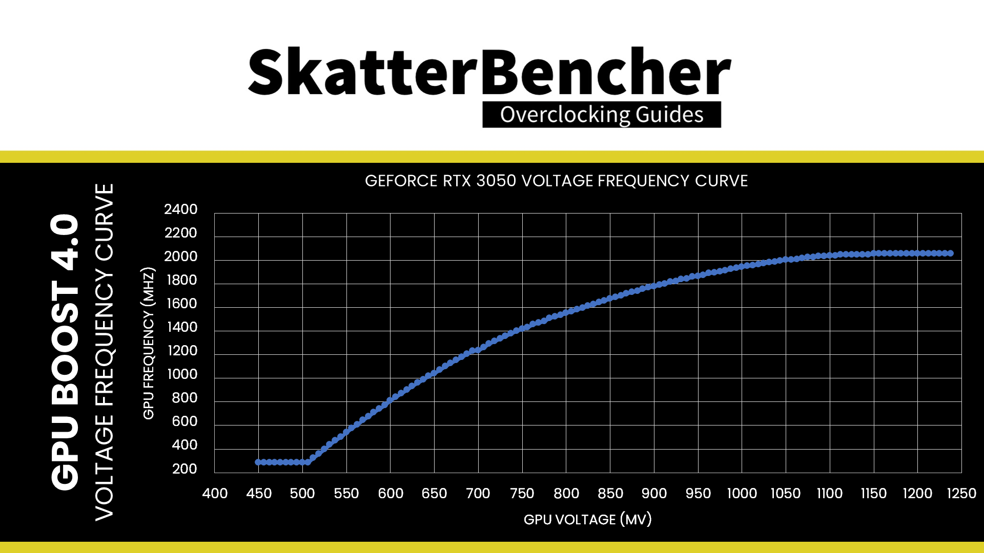
The NVIDIA GPU Boost technology uses power, current, and temperature inputs to evaluate the voltage headroom. It then uses the voltage frequency curve to select the appropriate performance point for a given situation.
Suppose the GPU uses too much power or current or has too high a temperature. In that case, the GPU Boost algorithm will select a performance point with a lower voltage and thus result in a lower operating frequency. Vice versa, if there’s sufficient headroom, the GPU Boost algorithm will select a higher performance point on the voltage frequency curve.
You can adjust the power, temperature, and voltage limits when overclocking. However, overclocking NVIDIA GPUs is not simply overriding the limits. While NVIDIA allows for customization for each of these limits, the limits are very conservative. For example,
- The Power Target on this RTX 3050 is set to its TBP of 130W. NVIDIA offers customization, but only between 77% and 112% of this target. So up to 145W.
- The Temperature Target can also be customized from the default value of 90 degrees Celsius to a minimum of 65 degrees Celsius and a maximum of 90 degrees Celsius.
- The GPU Voltage can also be customized from 0% to 100%

The GPU voltage, in particular, deserves special attention.
Since GPU Boost 2.0, NVIDIA defines two voltage limitations for its GPUs: the reliability voltage (Vrel) and the maximum overvoltage (Vmax).
- The reliability voltage (Vrel) is the highest voltage NVIDIA deems safe for use during the product-warranted period. Exceeding the reliability voltage means the GPU lifespan may be negatively impacted.
- The maximum overvoltage (Vmax) is the highest voltage NVIDIA allows for the GPU beyond the reliability voltage. While NVIDIA claims this overvoltage will impact GPU lifespan, it accepts that board partners and customers may be willing to take that risk.
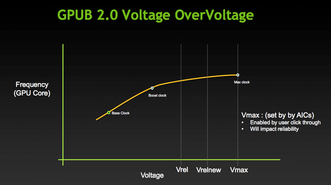
NVIDIA allows board partners to enable the voltage range up to Vmax for their customers in the VBIOS and enable customers to set voltage up to Vmax after acknowledging the risks.
The GPU Voltage option available in overclocking software represents the scale of overvoltage. 0% means no overvoltage allowed, and 100% means maximum overvoltage allowed.

Figuring out the Vrel and Vmax of your card is not easy. However, we can estimate it by checking the GPU voltage during a light 3D workload like the GPU-Z render test. For my RTX 3050, the reliability voltage is around 1.081V, and the maximum overvoltage is 1.10V. In other words, despite our voltage frequency curve going up to 1237.5 mV, the highest point on the voltage frequency curve used by the GPU Boost algorithm is 1081 mV.
Okay, now that we understand how NVIDIA GPU Boost 4.0 technology works, let’s get overclocking.
EVGA Precision X1
EVGA Precision X1 is an EVGA overclocking utility for NVIDIA graphics cards. Since its initial release in September 2018, it’s become a staple software tool within the PC enthusiast community.
The software enables control over 3D graphics performance and monitoring of your EVGA graphics card, including RGB control and other nifty tools. But the most relevant tools for our overclocking journey are access to the GPU Boost knobs and dials, including GPU and Memory frequency, Power Target, GPU Overvoltage, GPU Temperature Target, the OC Scanner, and VF Curve Tuner.
Overclocking the graphics card is simple. You increase the frequencies and check the stability in a range of benchmarks. But before we get to that, I need to say a quick word about the NVIDIA OC Scanner.
NVIDIA OC Scanner
The NVIDIA OC Scanner is part of the GPU Boost 4.0 toolset introduced with the Turing architecture in 2018. OC Scanner helps end-users automatically find the optimal overclocking settings. Using an NVIDIA-designed workload, the OC Scanner stress tests various points of the voltage-frequency curve.
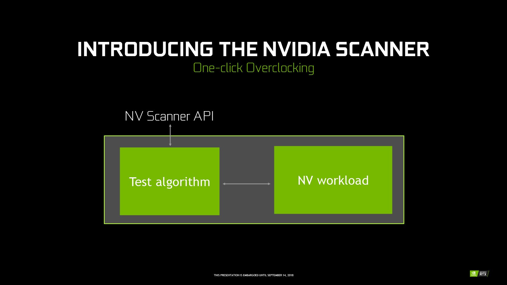
I had initially planned for the NVIDIA OC Scanner to be my first overclocking strategy, just like I did with the GeForce GT 1030 and GeForce GTX 1650 in SkatterBencher #40 and #42. However, it turned out there was almost no headroom. The overclocking result I achieved with the OC Scanner was identical to the out-of-the-box overclock of this EVGA graphics card.

To run the OC Scanner, you can use any third-party tool that supports the function, including the EVGA Precision X1 tool.
Upon opening the EVGA Precision X1 Tool
- Browse to the VF Curve Tuner menu
- Click on Scan
After the OC Scanner finishes, use the information from GPU OC and MEM OC to set the GPU Clock and Memory Clock. But, as I said, since the OC Scanner didn’t provide much improvement, I decided to go straight to manual overclocking.
OC Settings & Benchmark Results
Upon opening the EVGA Precision X1 tool
- Set Memory Clock to +1300
- Set GPU Clock to +200
- Set GPU Voltage to +100
- Set Power Target to 112
Then click Apply to confirm the overclocked settings.
We re-ran the benchmarks and checked the performance increase compared to the default operation.
- Geekbench 6 OpenCL: +14.05%
- Geekbench 6 Vulkan: +17.46%
- Furmark 1080P: +21.32%
- AI Benchmark: +11.53%
- 3DMark Night Raid: +10.33%
- 3DMark DLSS Feature Test: +21.12%
- Simple Raytracing: +19.55%
- Pure Raytracing: +20.10%
- Unigine Superposition: +22.50%
- Spaceship: +21.14%
- Handbrake: +0.14%
- Nero Score: +9.25%
- EZBench: +19.57%
- Shadow of the Tomb Raider: +19.15%
- CS:GO FPS Bench: +11.04%
- Final Fantasy XV: +18.88%
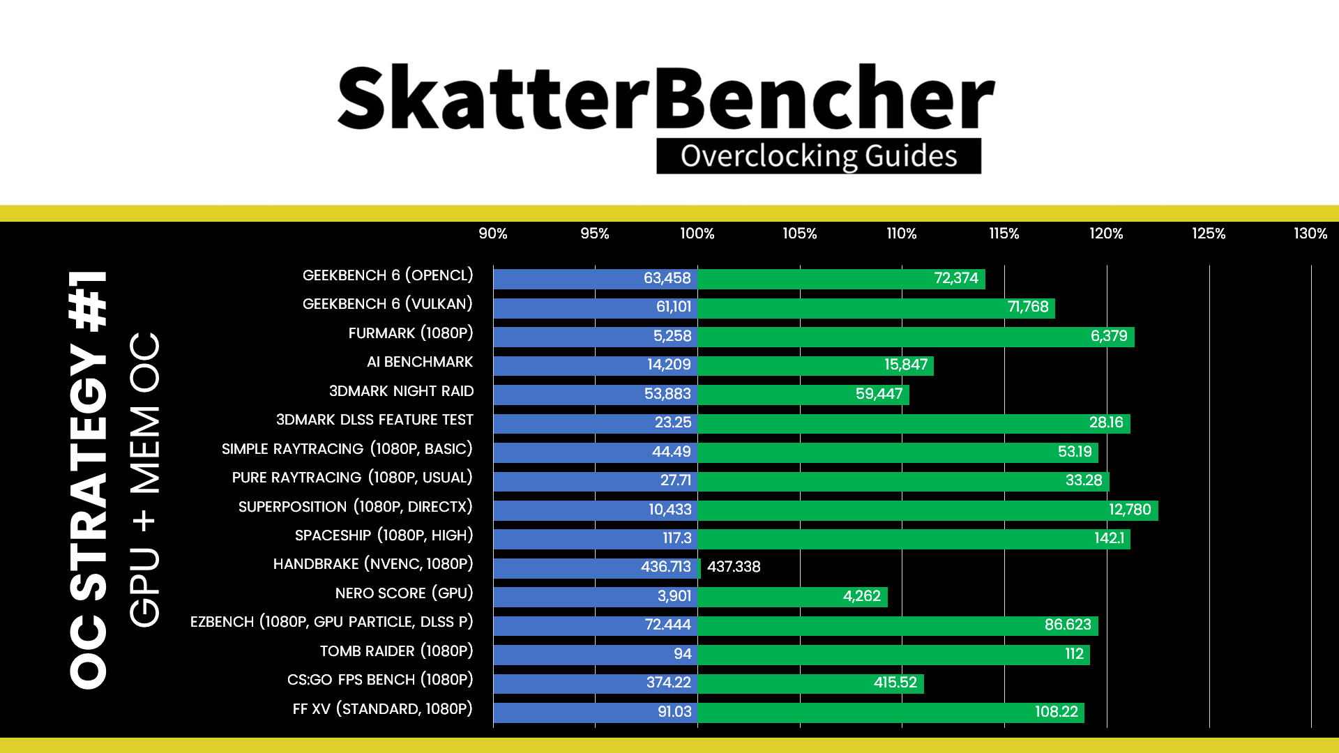
We substantially increase the benchmark performance by manually overclocking the GPU core and memory. The highest improvement is +22.50% in Unigine Superposition. To my surprise, the DLSS Feature Test performance also increased. To clarify, that means the increase in FPS with DLSS enabled goes up faster than with DLSS disabled.
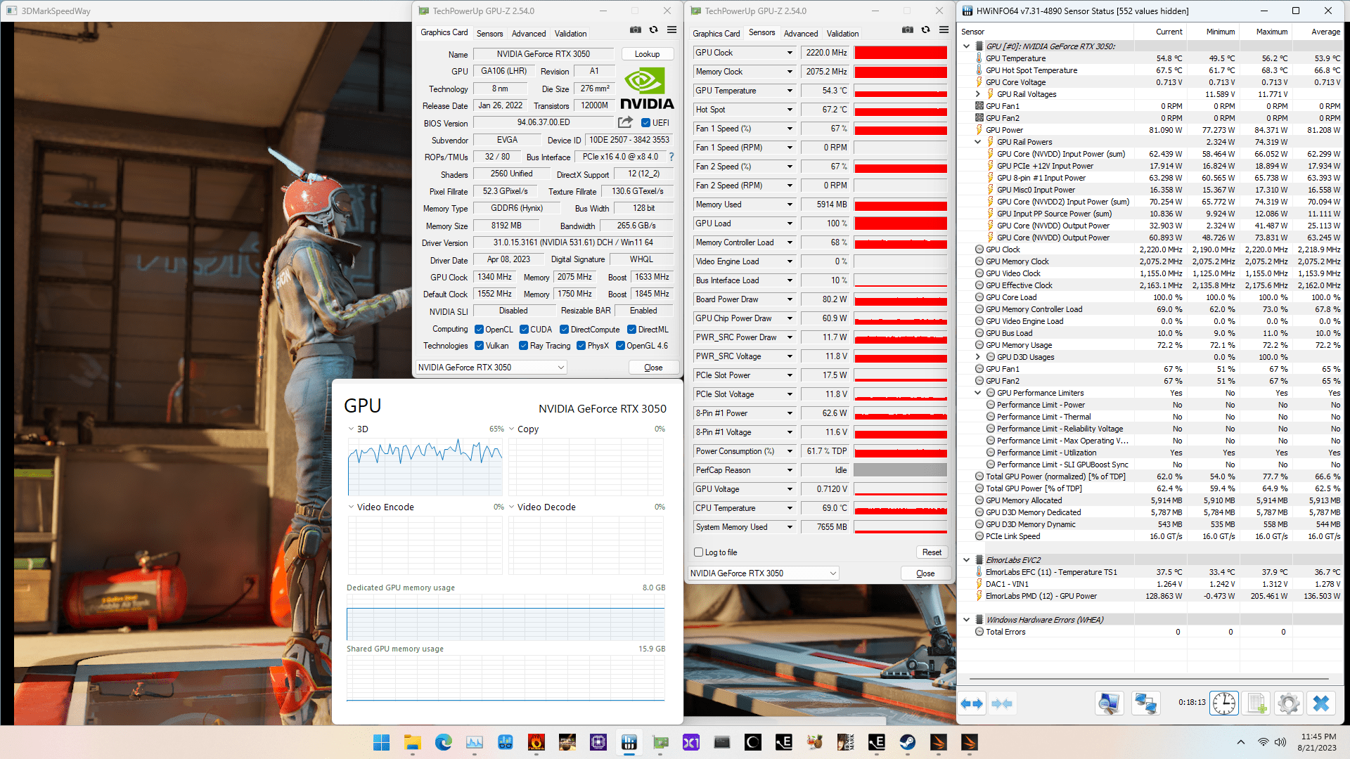
When running the GPU-Z Render Test, the maximum GPU Clock is 2235 MHz with 1.100V.
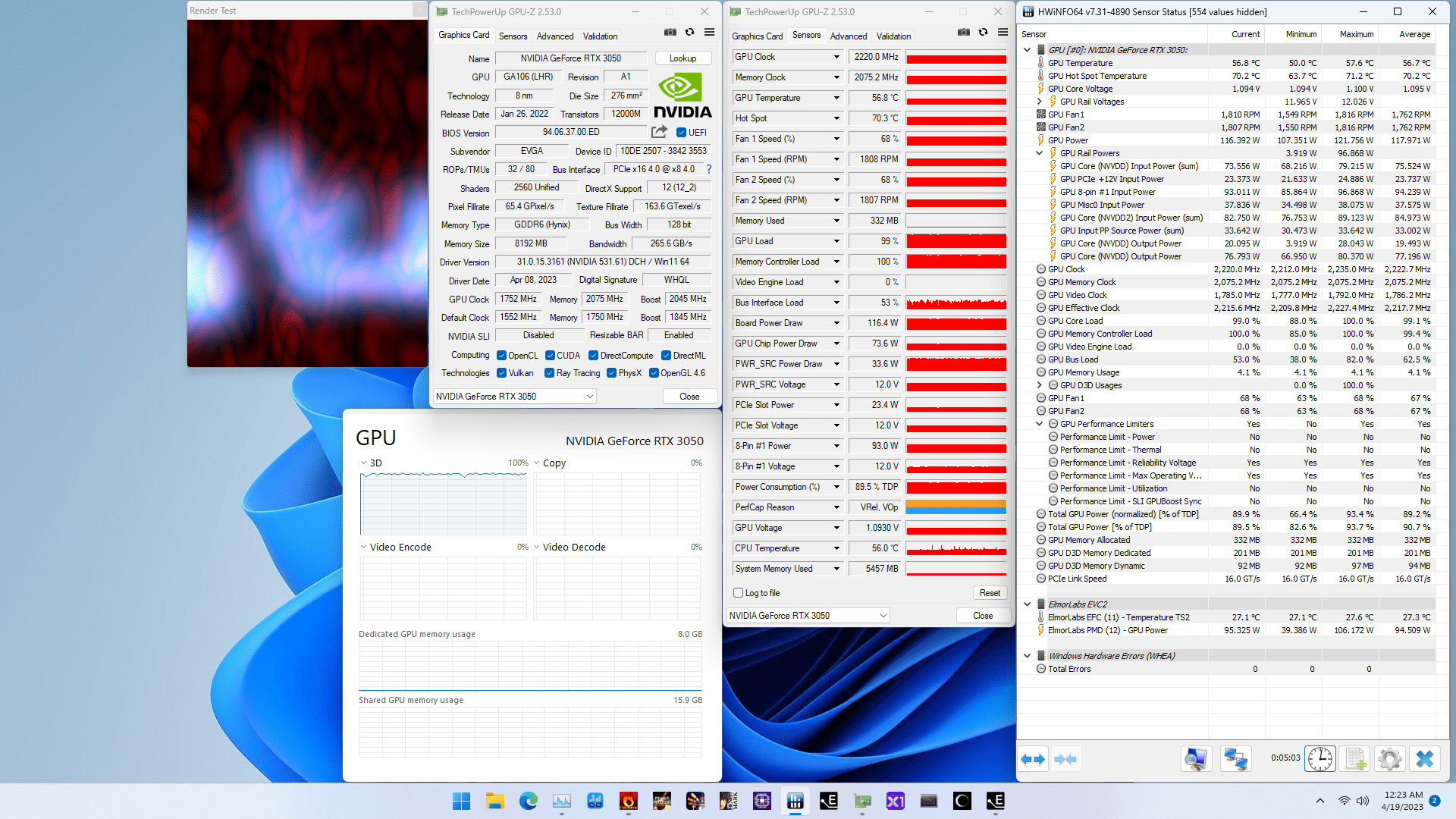
When running the 3DMark Speedway Stability Test, the average GPU effective clock is 2169 MHz with 1.060 volts, and the GPU Memory clock is 2075 MHz. The average GPU and GPU Hot Spot temperatures are 62.9 and 74.6 degrees Celsius. The average GPU power is 144.128 watts.
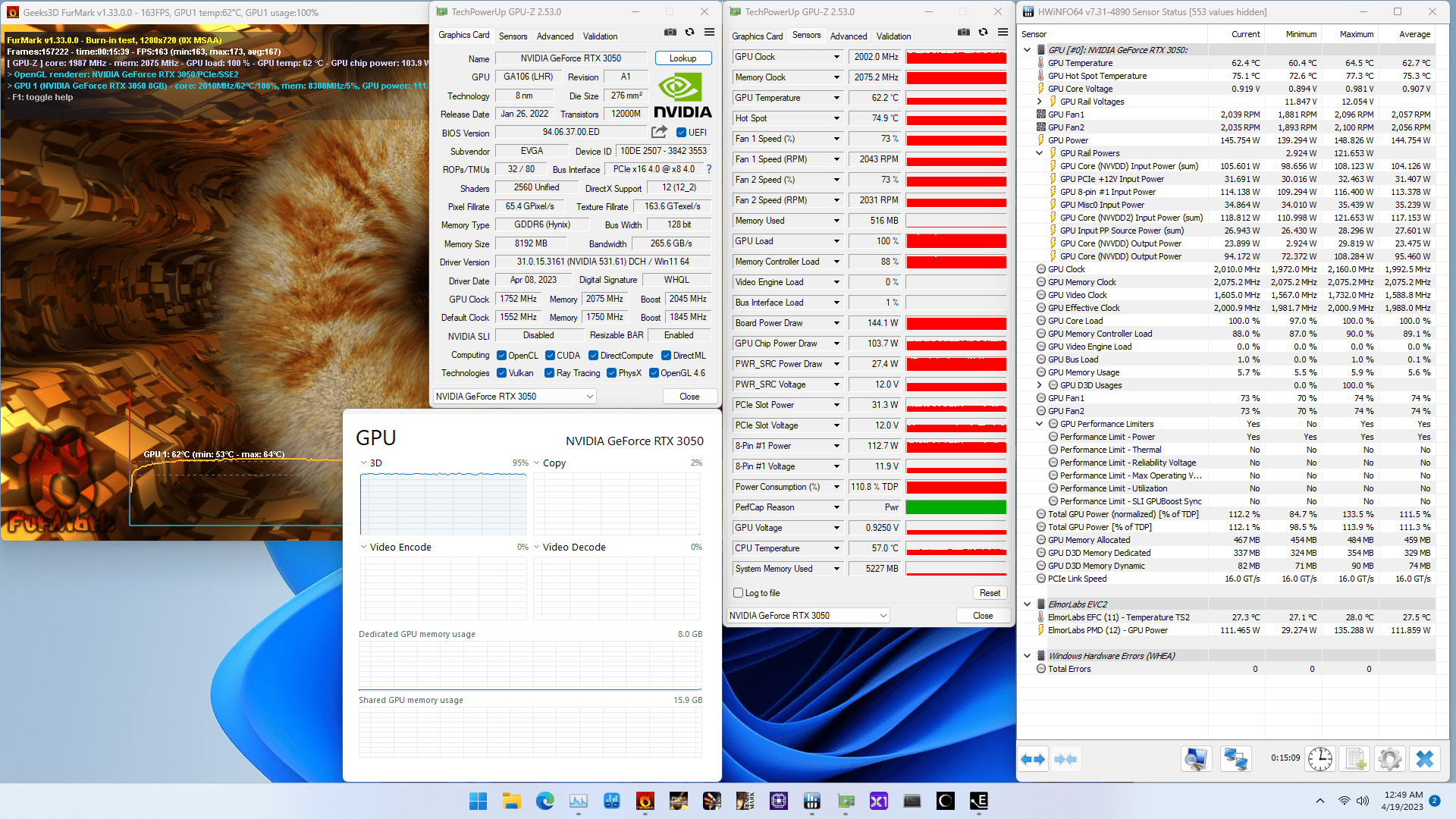
When running the Furmark GPU Stress Test, the average GPU effective clock is 1988 MHz with 0.907 volts, and the GPU Memory clock is 2075 MHz. The average GPU and GPU Hot Spot temperatures are 62.7 and 75.3 degrees Celsius. The average GPU power is 144.754 watts.
OC Strategy #2: Water Cooling & Shunt Modification
In our second overclocking strategy, we install water cooling and perform input power shunt modifications.
Bykski N-EV3060XC-X GPU BLOCK
It is my second time using a Bykski water block after the one I used on the A380. Since custom loop water cooling comes at a significant premium, we don’t usually find water blocks for low-end graphics cards like the RTX 3050. After comparing the PCBs of some other RTX 30 series graphics cards, I was lucky to find a block for the EVGA RTX 3060 XC physically compatible with this RTX 3050. But why on earth would I want custom loop water cooling in the first place?
For two main reasons:
- To eliminate any GPU temperature issues when overclocking, and
- To also water cool the VRM.
I don’t need to add much explanation to the first point: to increase the frequency, we need higher voltage, which will increase the GPU temperature. Liquid cooling will help alleviate that issue.
The second point is something I’ve brought up in previous discrete graphics overclocking guides. As we’ve seen with several discrete graphics cards I’ve overclocked on this channel, the VRM often becomes the main limitation for squeezing more performance out of the GPU. We saw this on the GT 1030, RX 6500 XT, Arc A380, and the A770. With the full-cover water block, the VRM components are actively cooled, and there should be less concern for the operating temperature when overclocking.
NVIDIA GPU Performance Limiters
Before we discuss the purpose of shunt modding, let’s first dig a little deeper into the topic of NVIDIA GPU overclocking. We discussed the GPU Boost overclocking technology and its overclocking knobs in the previous overclocking strategy. While these tools are helpful to increase the performance of your NVIDIA graphics card, you must also be aware of the various technologies that will limit your graphics card performance.
Like any other semiconductor vendor, NVIDIA employs many tools to govern the health and performance of the GPU at runtime. That includes tools to capture metrics and prevent damage due to out-of-spec behavior. NVIDIA is pretty secretive about the performance limiters. However, they provide some performance limiter debug information via the NVAPI.
NVAPI is NVIDIA’s core software development kit that allows direct access to NVIDIA GPUs and drivers on all Microsoft Windows platforms. Applications such as EVGA Precision X1 or HWiNFO rely on this API to provide us, enthusiasts, with GPU performance information. Let’s open HWiNFO and look at the various Performance Limiters available.
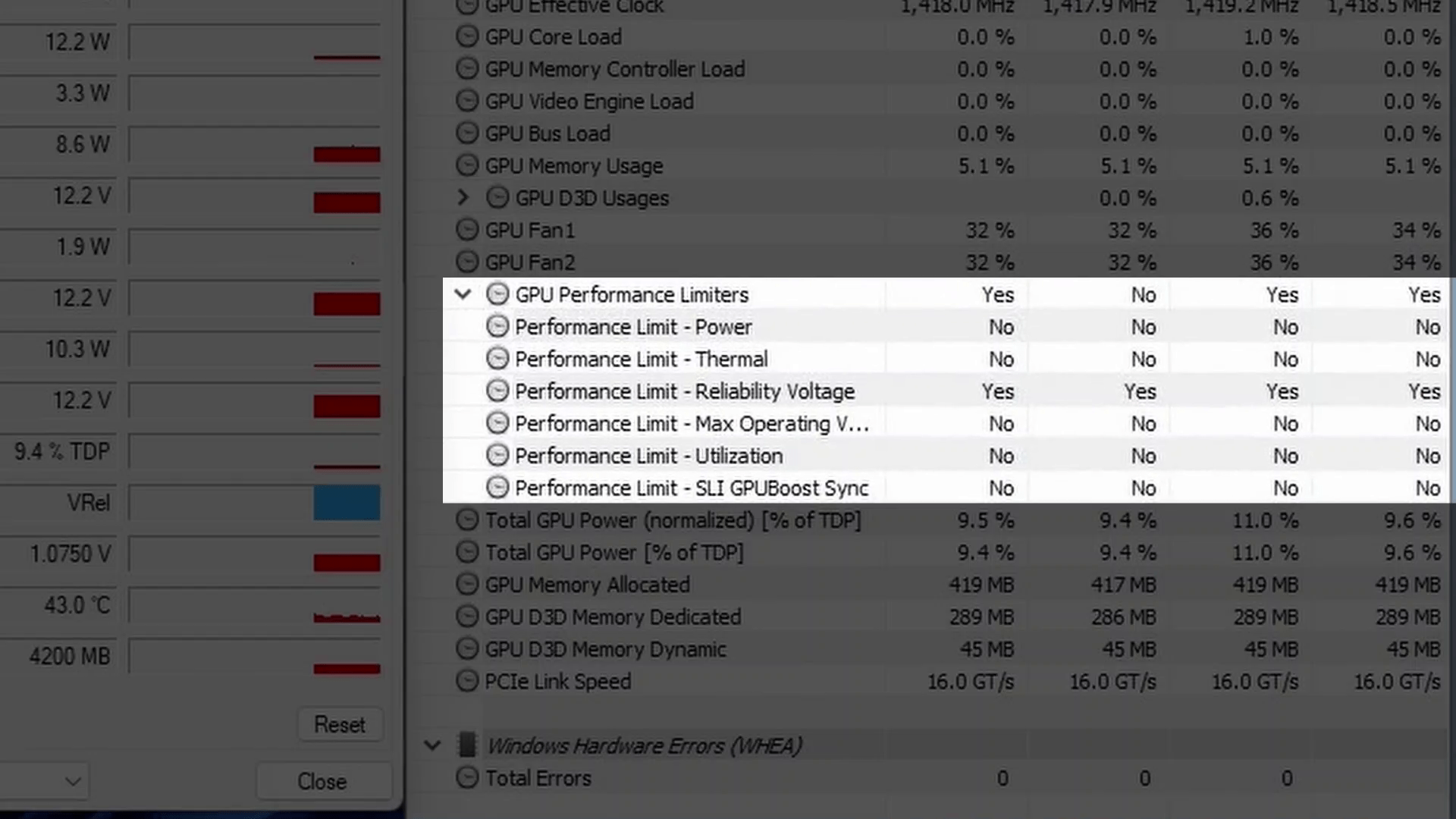
- Power: The Power performance limiter is flagged if the graphics card is using the maximum allowed power consumption
- Thermal: The Thermal performance limiter is flagged if the graphics card is hitting the maximum allowed temperature
- Reliability Voltage: The Reliability Voltage performance limiter is flagged if the GPU requests the Vrel voltage to the voltage controller.
- Max Operating Voltage: The Maximum Operating Voltage performance limiter is flagged if the graphics card allows GPU voltage beyond the reliability voltage and the GPU requests the Vmax voltage to the voltage controller.
- Utilization: The Utilization performance limiter is flagged when all GPU compute resources are currently in use.
- SLI GPUBoost Sync: The SLI GPUBoost Sync performance limiter is flagged when the GPU Boost frequency is limited by multi-GPU SLI frequency synchronization.
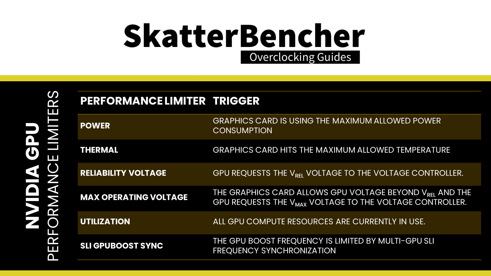
Note that many more undocumented performance limiters are likely impacting the graphics card’s performance. We will get to that topic in due time. For now, suffice it to say that when we try to get the maximum performance, our goal is to have the maximum operating frequency when only the Utilization performance limiter is flagged.
From the stability tests of the previous overclocking strategies, we know that the following performance limiters are triggered:

So, clearly, for any kind of real-world 3D workload, the performance is limited by the maximum allowed power consumption. So, let’s look at how the power consumption of the NVIDIA RTX 3050 is managed.
GPU Power Measurement
Broadly speaking, modern graphics cards can impose power consumption limits in three ways.
First, like on most low-end and older generation graphics cards, the GPU can estimate power consumption based on the workload characteristics and the assumed voltage based on the voltage-frequency curve. This technique is present on older, low-end NVIDIA graphics cards, and I explained how they work when I overclocked the GeForce GT 1030 and GeForce GTX 1650.
Second, like on most modern AMD graphics cards, the GPU can rely on the external voltage controllers to report the power consumption to the GPU. I explained how this method works when I overclocked the Radeon RX 6500 XT and Arc A770.
Third, like on most mid-end and high-end NVIDIA graphics cards, a separate hardware circuit is used to directly measure the input power and report it to the GPU.
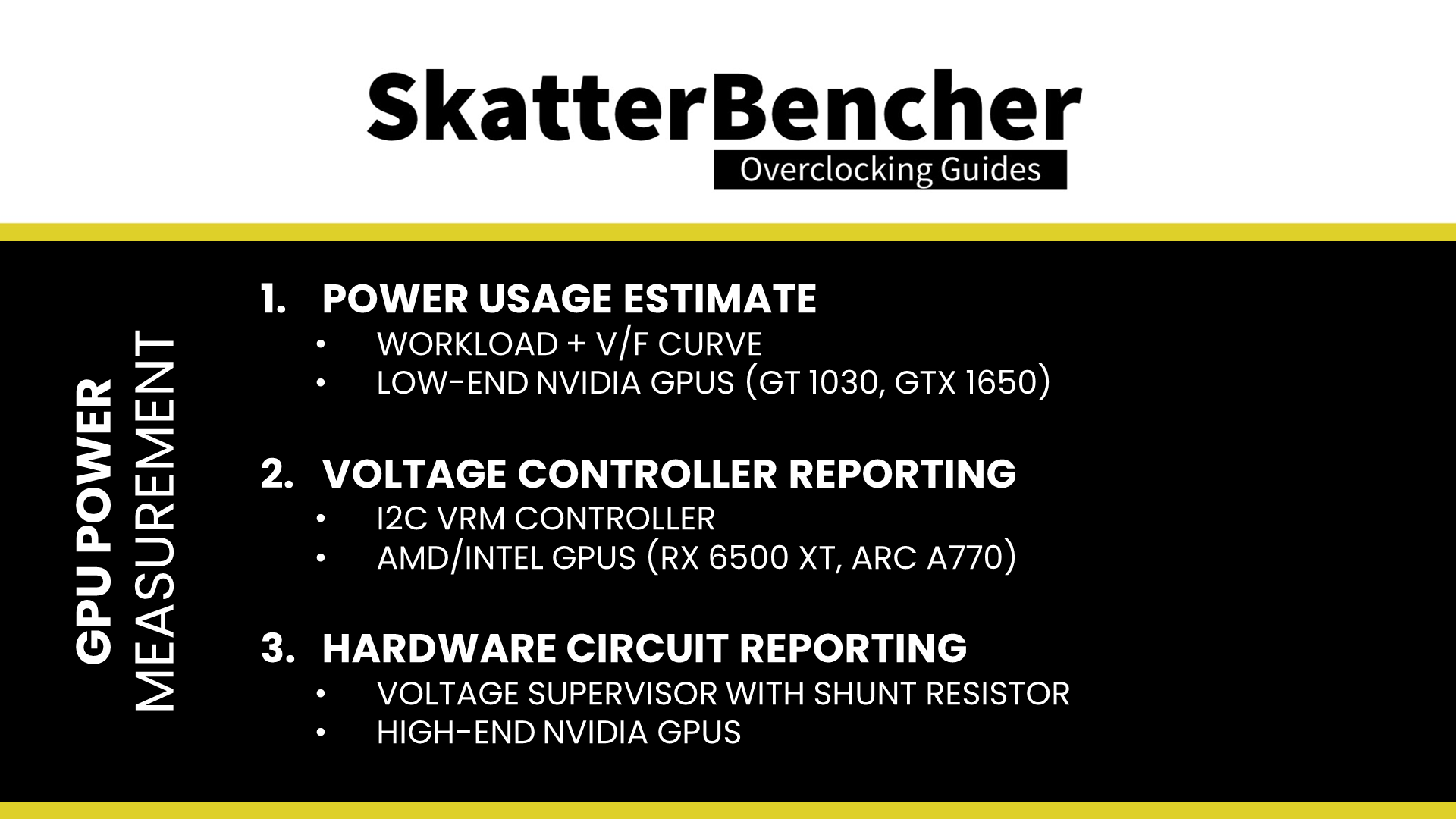
Or, as we will find out in a bit, it can be a combination of these three methods. Let’s look at the EVGA GeForce RTX 3050 XC GAMING PCB and see the situation.
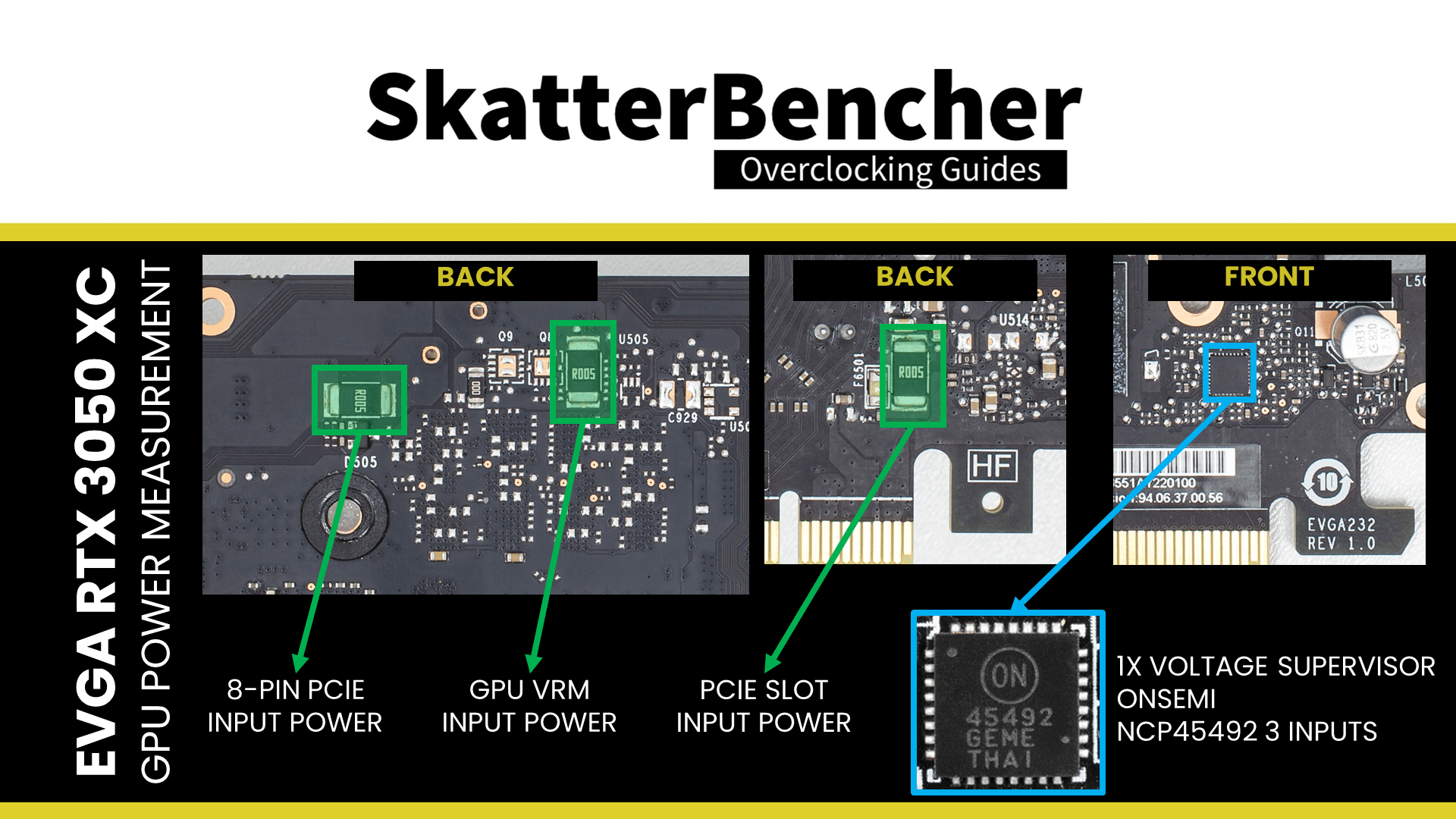
EVGA GeForce RTX 3050 XC GAMING PCB Power Regulation
The VRM design of the EVGA GeForce RTX 3050 XC GAMING consists of the following major components.
The GPU is powered by a 4-phase design managed by uPI Semiconductor uP9512R digital multi-phase PWM controller. This controller drives four (4) Alpha and Omega AOZ5312UQI 60A DrMOS, one for each phase.
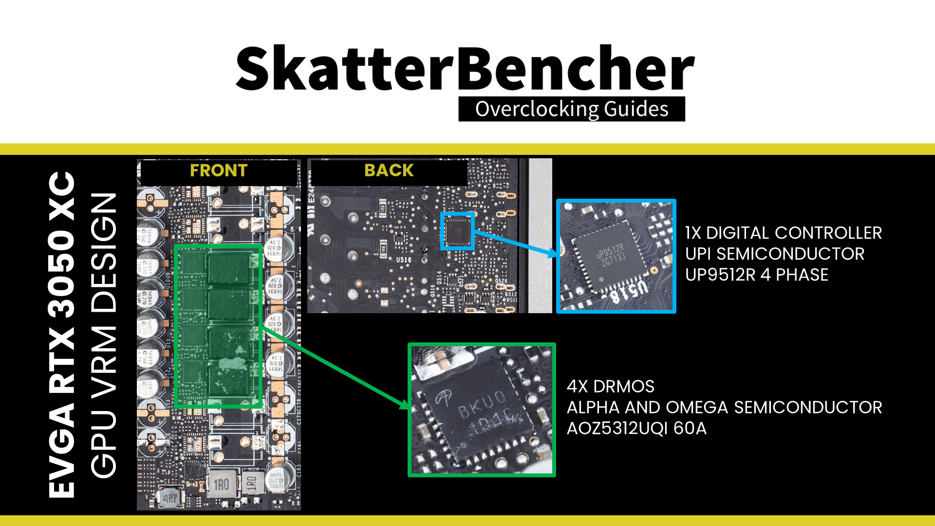
DrMOS is a power delivery solution that integrates the MOSFET driver directly on-chip with the power FETs. Funny tidbit: Intel wrote the DrMOS 1.0 specification back in 2004.
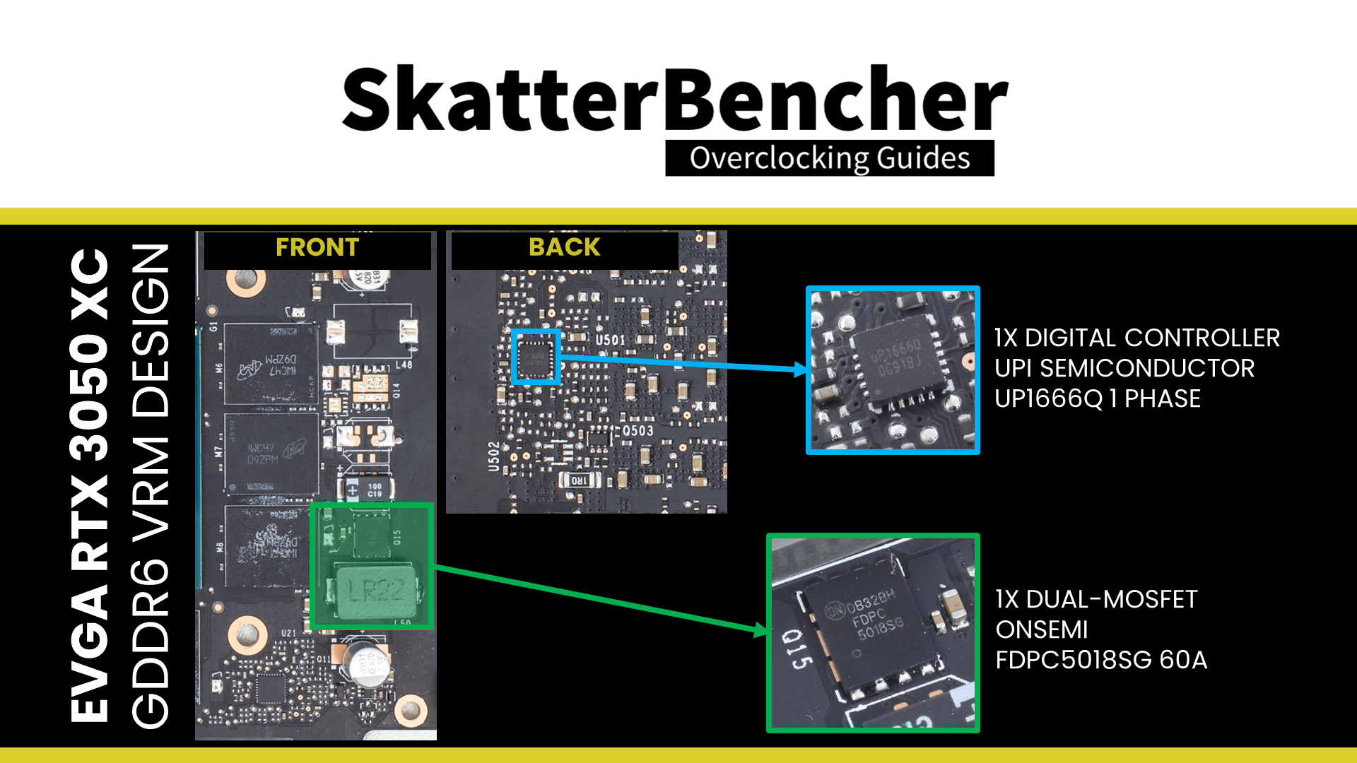
The GDDR6 memory is powered by a single-phase design managed by the uPI Semiconductor uP1666Q multi-phase PWM controller. This controller drives a single (1) Onsemi FDPC5018SG 70A dual-MOSFET.
The GPU power measurement circuit is managed by the Onsemi NCP45492 voltage supervisor. This IC can simultaneously monitor voltage, current, and power on up to four high-voltage power supplies. This IC provides the GPU information about the PCIe plug and slot input power.
EVGA GeForce RTX 3050 XC GAMING PCB Shunt modding
There are two ways to override the power limit of a graphics card: flashing a VBOS with a higher power limit or a physical modification to the graphics card.
Flashing an NVIDIA VBIOS with different values than stock is notoriously difficult. Not only is it challenging to find a software tool that allows the flashing of a VBIOS, but even if you can flash the BIOS, it’s impossible to modify the BIOS yourself as the VBIOS is digitally signed. You can only have a higher power limit if an “XOC” VBIOS is available from an AIB vendor.
The physical modification for mid-end and high-end NVIDIA graphics cards involves shunt modding. A current shunt is a resistor that generates a slight, measurable voltage depending on the current flow. This yields a real-time power measurement, which the voltage supervisor IC reports to the GPU. The GPU, in return, uses this as one of the inputs for power management.
We can tamper with this power monitoring circuit to report less than the actual current flow. The process is straightforward: We simply add more shunt resistors over the existing ones. We modify three shunt resistors: two at the top and one at the bottom of the card. The shunt resistors are used to measure
- The input power from the PCI-e 8-pin connector
- The input power from the PCI-e slot
- The input power to the GPU Core voltage regulator
They’re all 5 milli-ohm shunt resistors. Our modification adds an identical 5 milli-ohm shunt resistor, doubling the resistance across the shunt and halving the measured input power.
OC Settings & Benchmark Results
We apply the same overclocking settings as in the previous overclocking strategy.
Upon opening the EVGA Precision X1 tool
- Set Memory Clock to +1300
- Set GPU Clock to +200
- Set GPU Voltage to +100
- Set Power Target to 112
Then click Apply to confirm the overclocked settings.
We re-ran the benchmarks and checked the performance increase compared to the default operation.
- Geekbench 6 OpenCL: +22.87%
- Geekbench 6 Vulkan: +22.67%
- Furmark 1080P: +23.15%
- AI Benchmark: +15.55%
- 3DMark Night Raid: +12.05%
- 3DMark DLSS Feature Test: +21.51%
- Simple Raytracing: +20.16%
- Pure Raytracing: +23.06%
- Unigine Superposition: +23.23%
- Spaceship: +21.31%
- Handbrake: +0.77%
- Nero Score: +8.87%
- EZBench: +19.77%
- Shadow of the Tomb Raider: +18.09%
- CS:GO FPS Bench: +16.03%
- Final Fantasy XV: +19.82%
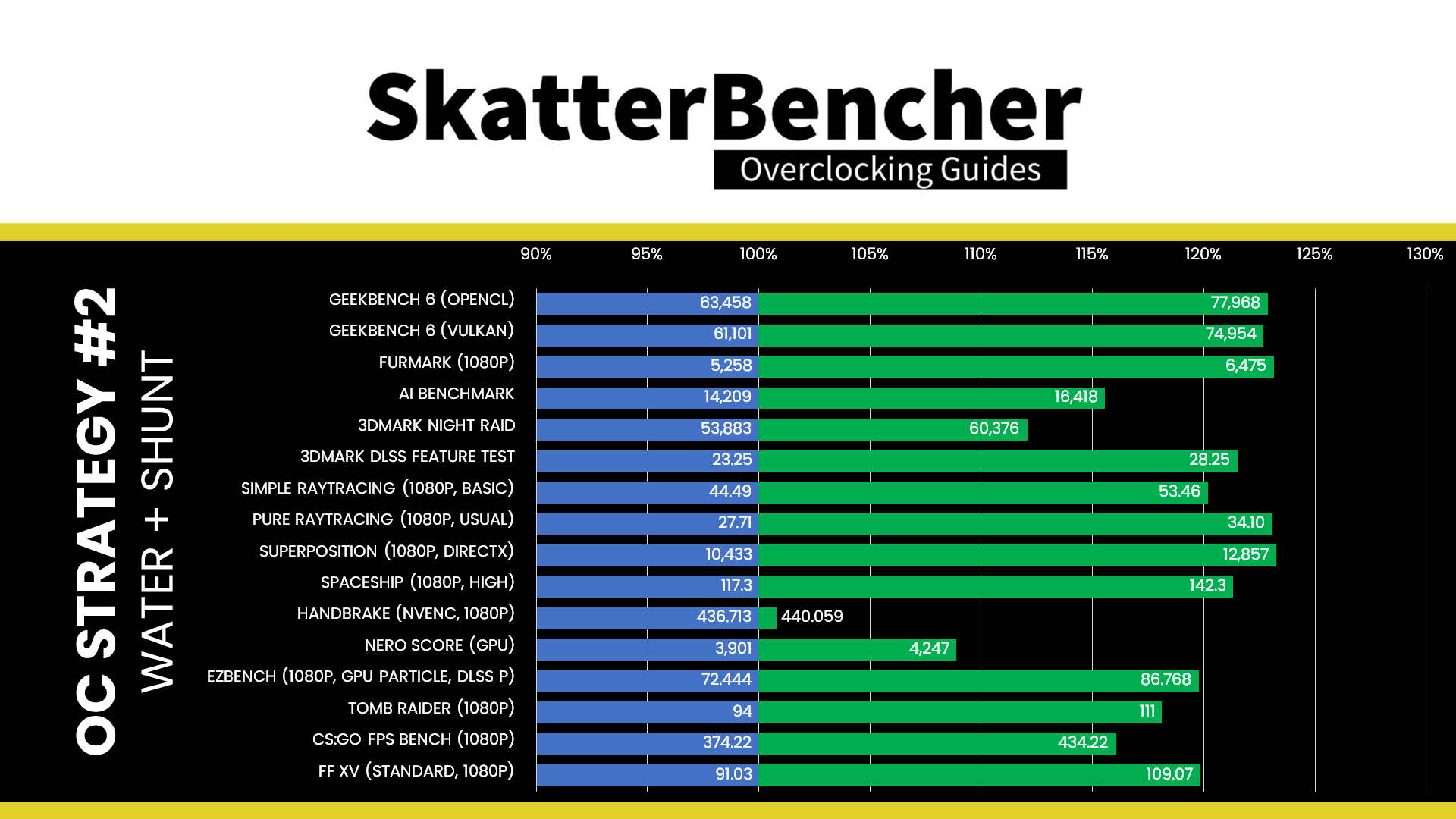
By eliminating the input power limit and improving the operating temperature, we get a further performance boost in almost all benchmarks. We see the highest performance increase of +23.23% in Unigine Superposition.
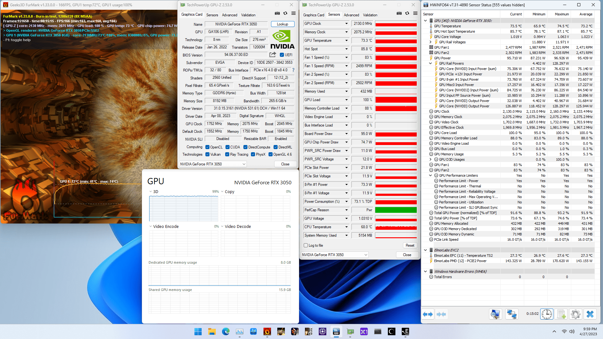
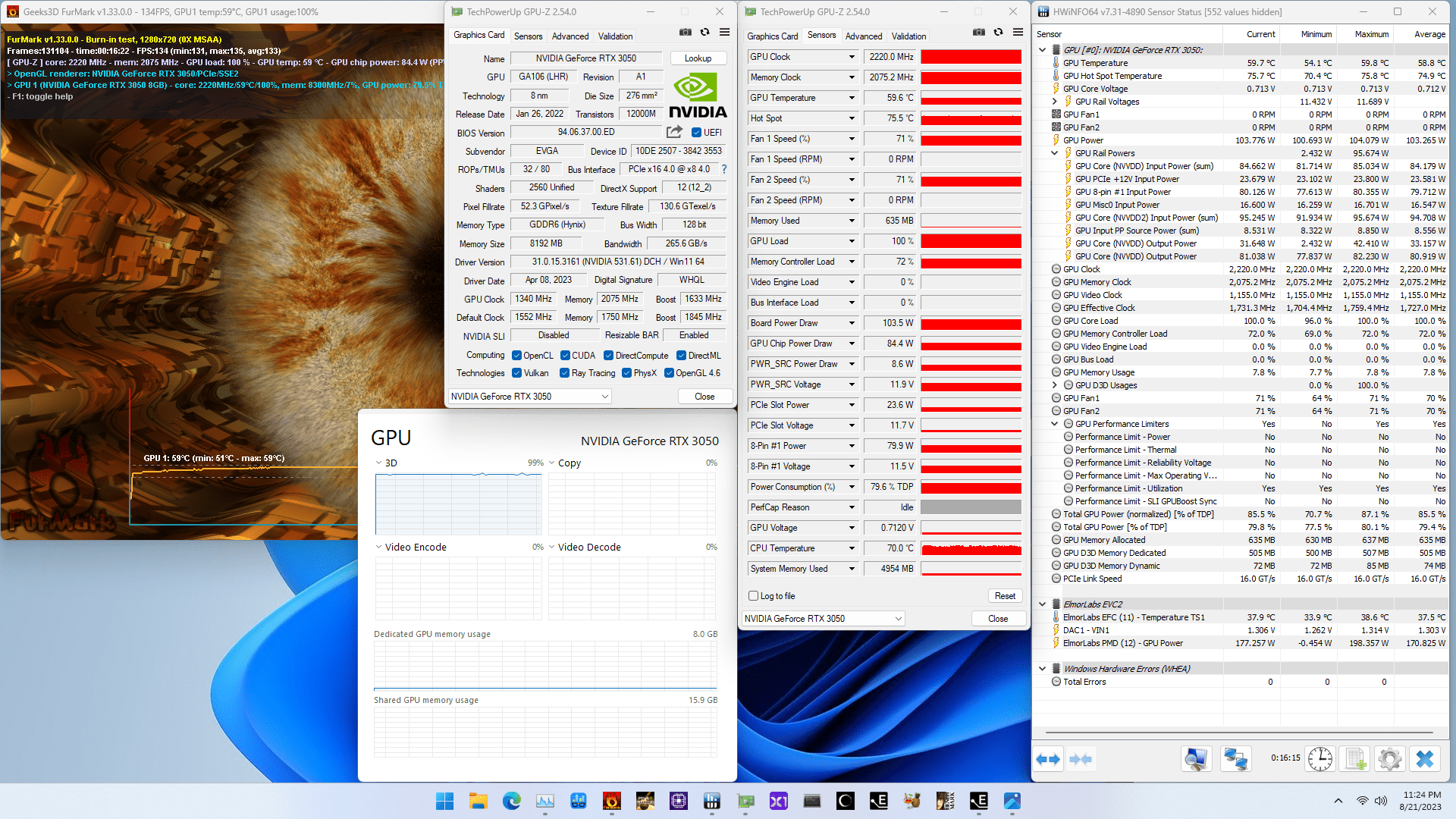
When running the GPU-Z Render Test, the maximum GPU Clock is 2212 MHz with 1.094V.

When running the 3DMark Speedway Stability Test, the average GPU effective clock is 2132 MHz with 1.100 volts, and the GPU Memory clock is 2075 MHz. The average GPU and GPU Hot Spot temperatures are 65.7 and 78.1 degrees Celsius. The average GPU power is an estimated 156.302 watts.

When running the Furmark GPU Stress Test, the average GPU effective clock is 1967 MHz with 1.100 volts, and the GPU Memory clock is 2075 MHz. The average GPU and GPU Hot Spot temperatures are 73.2 and 85.7 degrees Celsius. The average GPU power is an estimated 190.878 watts.
OC Strategy #3: ElmorLabs EVC2 & Hardware Modifications
As you’ll see in a minute, when we evaluate the results from our previous overclocking strategy, we find that two elements are still limiting the overclocking potential of the RTX 3050 GPU: power and voltage.
So, in our third and final overclocking strategy, we call upon the help of Elmor and his ElmorLabs EVC2 device. We resort to hardware modifications to work around the remaining power and voltage limitations of the RTX 3050 graphics card.
I will elaborate on two distinct topics:
- Why do we need and use hardware modifications?
- How we use the ElmorLabs EVC2SX for the hardware modifications?
Situation Analysis: Power
We tried to overcome the power performance limiter in the previous overclocking strategy. Let’s have a closer look to see whether we were able to achieve this.
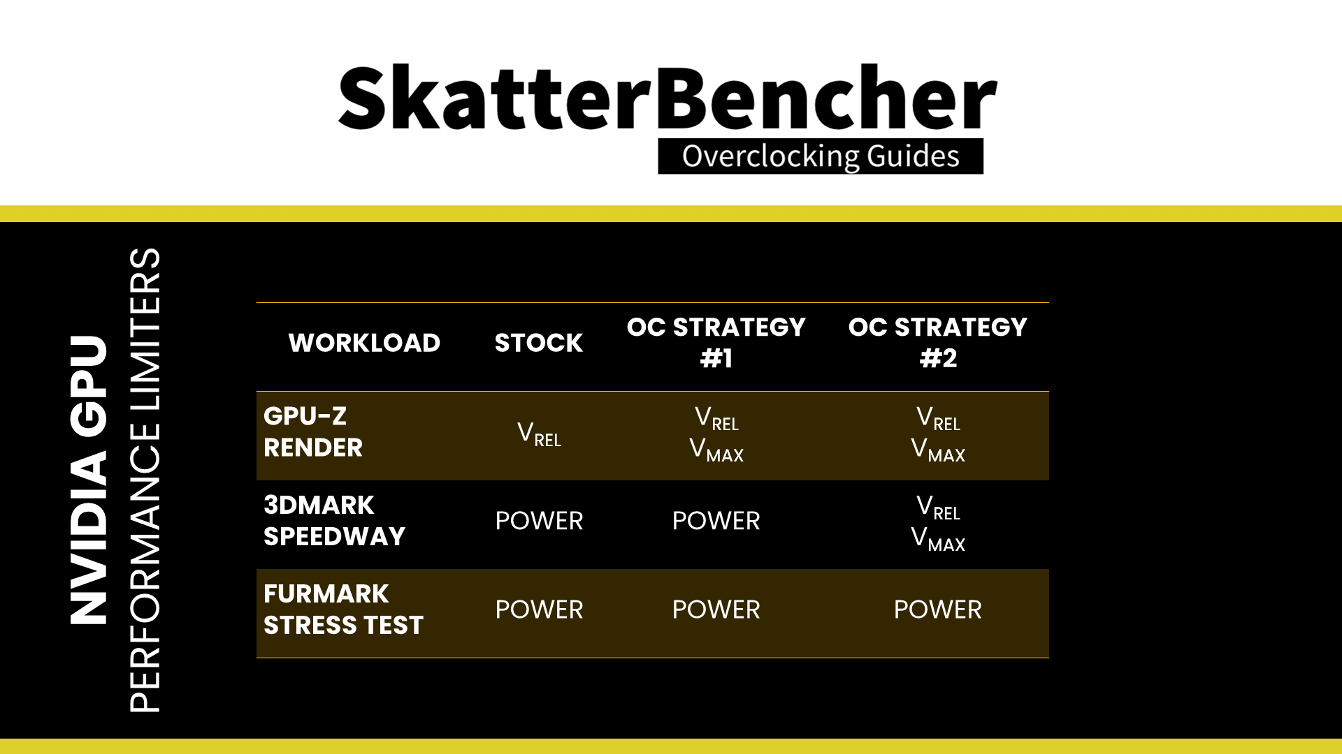
As expected, in 3DMark Speedway, we could work around the power limitation by shunt modding. The main performance limiter is the maximum allowed GPU voltage. However, against our expectations, in Furmark, the power performance limiter is still flagged despite shunt modding. That’s weird!
We can again rely on the NVAPI and HWiNFO to investigate what’s happening. Let’s have a look at the GPU Power reporting. I won’t go over the details of each line item, but let’s compare all rails with NVVDD during the Furmark Stress Test.
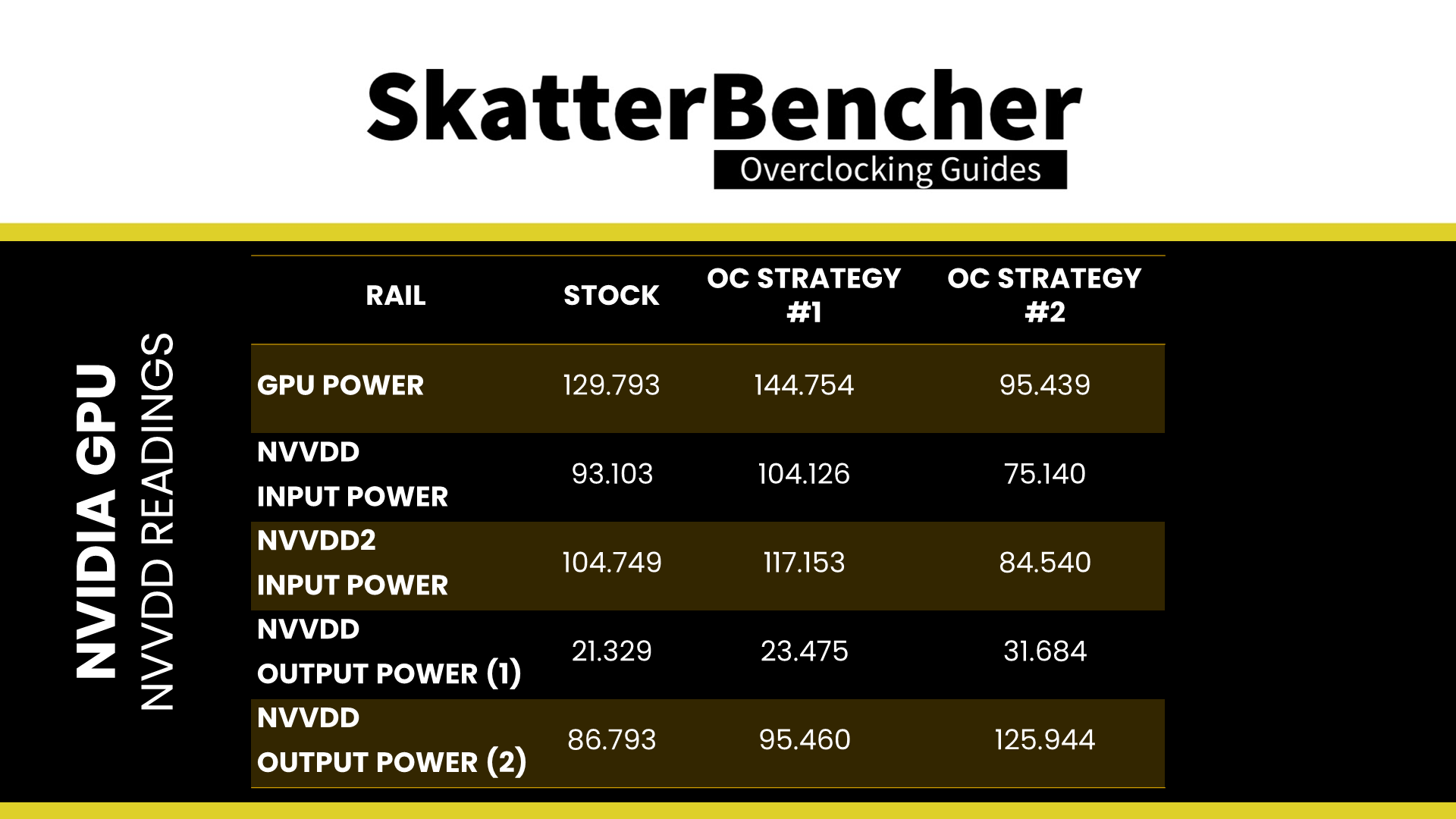
As you can see from the comparison, shunt-modding effectively lowered the reported input power. However, it did not adjust the two output power metrics. So, we can theorize that the output power metrics are causing the power performance limiter to be flagged.
There’s not much information available on what this metric is. Still, we can speculate this is a calculated power (W=V*A) output based on the current GPU VID (voltage) and the workload characteristics (current). We will put this theory to the test when we do the voltage modification. Let’s return to our GPU voltage controller to discuss the voltage modification.
GPU Voltage Controller – uPI Semi uP9512R
We identified the uPI Semiconductor uP9512R as the GPU voltage controller.
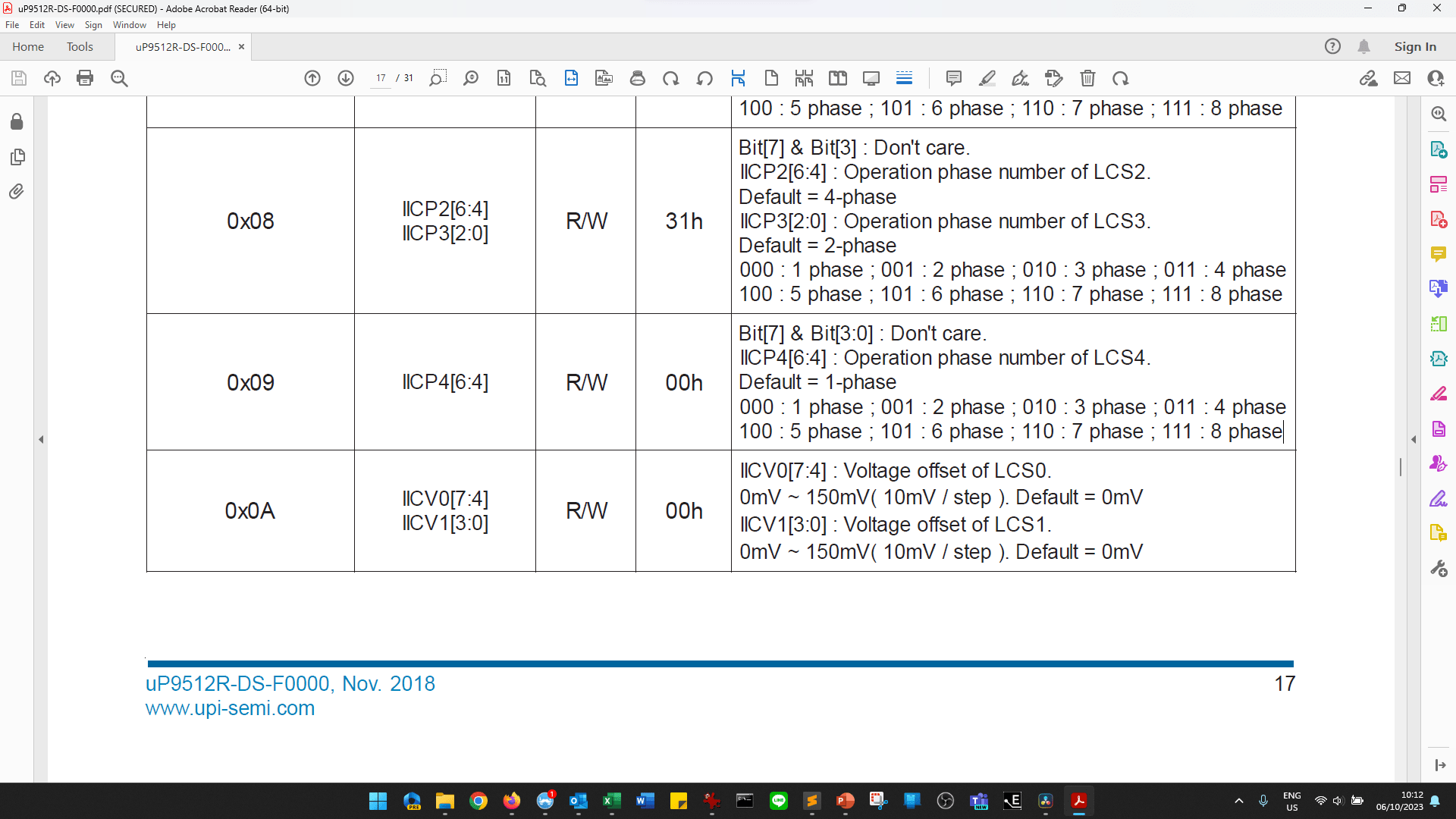
The uPI Semiconductor uP9512R supports NVIDIA’s Open VReg Type 4i+ with PWMVID Interface and has an SMBus Interface. That means we have two means of manually adjusting the output voltage: digitally, by using the SMBus interface, and analogly, by modifying the PWMVID circuit.
Digital Voltage Control
A quick read through the datasheet reveals how this controller provides I2C access. This is our starting point for the hardware modification. Unfortunately, there’s no place to add a simple I2C pin header. So, we must solder cables directly to the PCB to connect the three I2C pins: SCL, SDA, and GND.

This allows us to communicate directly with the onboard digital voltage controller. We can then connect the EVC2 device to the I2C pins to control the voltage regulator. Reading through the voltage controller datasheet provides a lot of good information. For example, there is a function called Voltage Offset, which allows for up to +150mV overvoltage. So, we can try this to increase the GPU voltage above the maximum operating voltage.
Unfortunately, it didn’t seem to help improve the performance. We’ll get back to that later in this video.
Analog Voltage Control
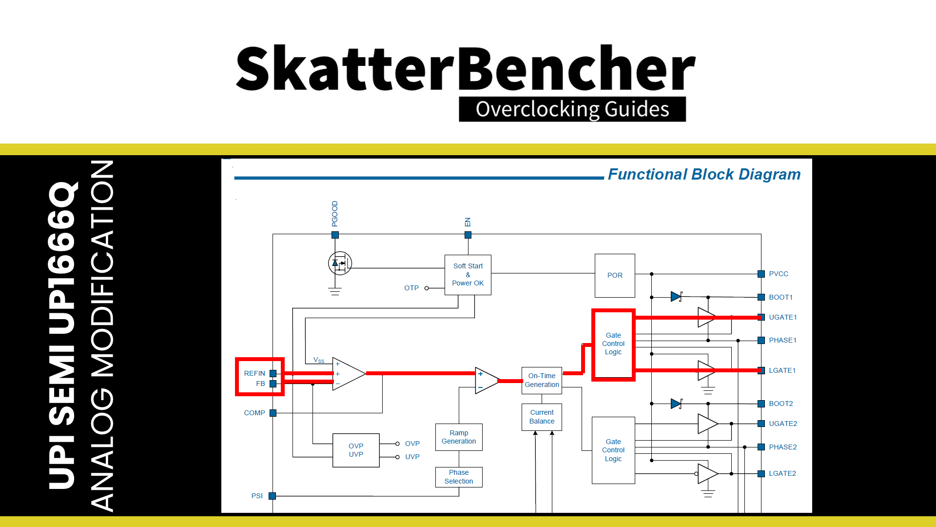
In the datasheet, we find a Typical Application Circuit where we can trace Vout via the DrMOS to the PWMx of the voltage controller. PWMx indicates the phase number of operation is flexible for this controller. The controller outputs a PWM logic signal to the external MOSFET driver via these pins. On the uP9512, these are pins 4 to 11.

In the Functional Block Diagram, we find that the difference between the Error Amplifier (EAP) and Feedback voltage (FB) drives the PWM Control Logic. If we dig deeper, we find that EAP is nothing more than the Reference Input Voltage (REFIN) with Vdroop adjustment.
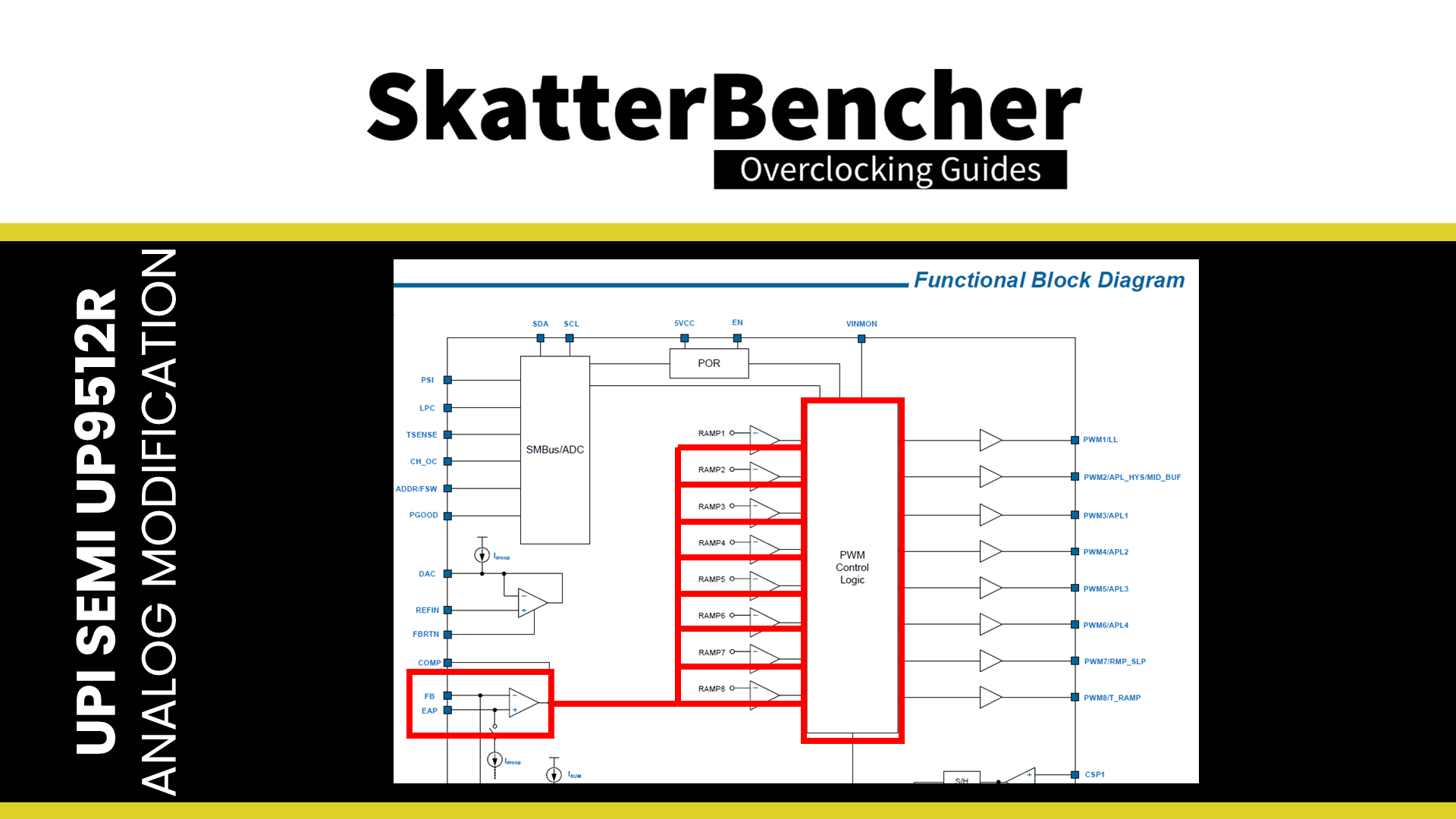

So, we could also say that the difference between the Reference Input Voltage (REFIN) and the Feedback voltage (FB) drives the PWM Control Logic.

The voltage controller aims to have the reference input (REFIN) equal to the sensed output voltage (FB). Suppose the reference input voltage is higher than the feedback voltage. In that case, the voltage controller will try to increase the output voltage. Suppose the reference input voltage is lower than the feedback voltage. In that case, the voltage controller will try to decrease the output voltage.
That offers us two ways to control the output voltage: adjust the REFIN or the FB.
The Functional Description section provides a more detailed overview of the PWMVID Structure, which configures REFIN. The figure shows that VREF, REFADJ, and VID affect the REFIN voltage. In short, resistors R2, R3, R4, and R5 set a Boot voltage from the 2V reference voltage (Vref). This voltage can dynamically be adjusted by a REFADJ output, which is determined, in this case, by the VID. The VID is, of course, controlled by our GPU and its GPU Boost algorithm.
So, what are our options to manually adjust the reference input voltage (REFIN)? Let’s check Ohm’s Law: Voltage = Current x Resistance
- We replace any of the four aforementioned resistors with a different resistor. Reducing the resistance of R2 or R3 would increase the REFIN, whereas lowering the resistance of R4 or R5 would decrease the REFIN.
- Instead of replacing the resistor, we can add a variable resistor parallel with any of the four mentioned resistors, which will effectively decrease the resistance of that resistor. That is the typical approach for hardware modifications, as we can use a variable resistor to change the voltage on the fly.
- We can inject current at the REFIN point, which increases the voltage to REFIN.


With the ElmorLabs EVC2, we go for the third option as we alter the current in the circuit to change the reference input voltage. That will enable us to increase the operating voltage beyond NVIDIA’s reliability and maximum operating voltage limit.
We have two options to increase the voltage: offset or fixed. In offset mode, we add a voltage to the GPU VID request. We ignore the GPU VID request in fixed mode and apply a static voltage.
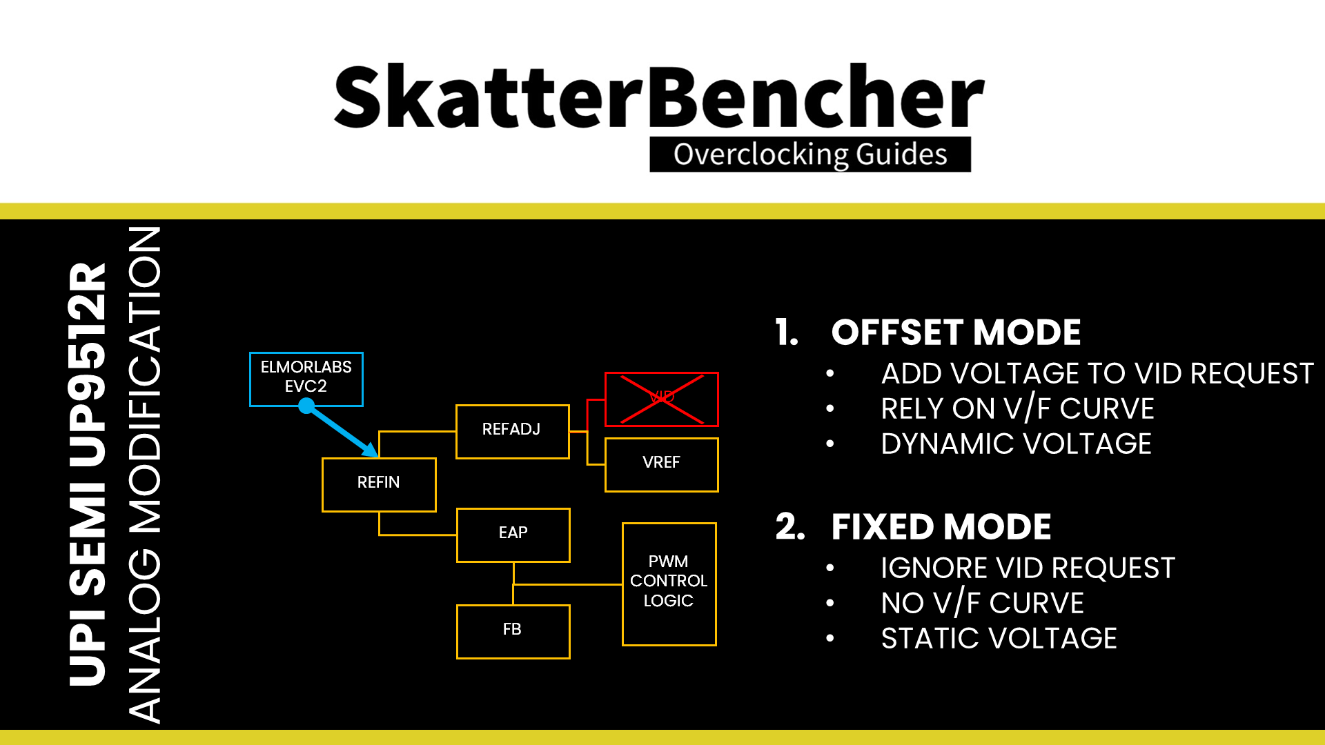
In our case, we must opt for the fixed voltage mode to address the power performance limiter. As a quick reminder, the theory is that a power performance limiter estimates GPU output power based on current GPU VID (voltage) and workload characteristics (current). We can force the GPU to use a very low VID to work around this issue and then apply a fixed output voltage to ensure GPU stability.
So, in addition to the modification to increase the voltage, we also remove the resistor connecting the REFADJ and VID from interfering in the circuit. That prevents the GPU from talking to the voltage controller.

Memory Voltage Controller – UPI uP1666Q
We identify the uP1666Q IC as the memory voltage controller.
Regular viewers will know we previously encountered this IC when overclocking the GeForce GT 1030. Unlike the GPU voltage controller, this one doesn’t support I2C; thus, we only have the option of analog voltage modification.
In the datasheet, we find a Typical Application Circuit and can trace the voltage output (Vout) to UGATE and LGATE. The Upper Gate Driver Output (UGATE) and Lower Gate Driver Output (LGATE) connect to the high-side and low-side MOSFETs.

To keep it simple, the MOSFET is a transistor controlled by the GATE signal that will switch on and off. In this case, the high side connects to 12V, and the low side would be 0V as it’s connected to ground. The MOSFET outputs this 12V and 0V through an output filter, which averages out these voltages to provide a smooth output voltage.
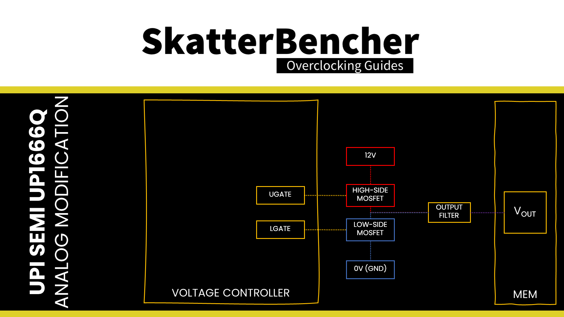
For example, the MOSFET switches on the high-side (12V) 10% of the time and the low-side (0V) 90% of the time. The average voltage output of the MOSFET is then 12V x 10% + 0V x 90% = 1.2V.
The voltage controller can control the output voltage by sending more or fewer signals via the upper or lower gate. An increase in signals through the UGATE tells the MOSFET to switch on the high side more often, increasing the output voltage.
In the Functional Block Diagram, we find that the difference between Reference Input voltage (REFIN) and Feedback voltage (FB) drives the Gate Control Logic. The voltage controller aims to have the reference input equal to the sensed output voltage. Suppose the reference input voltage is higher than the feedback voltage. In that case, the voltage controller will try to increase the output voltage. Suppose the reference input voltage is lower than the feedback voltage. In that case, the voltage controller will try to decrease the output voltage.
That offers us two ways to control the output voltage: adjust the REFIN or the FB.
Under Functional Description, we find a more detailed overview of the Voltage Control Loop. The figure shows that VREF, REFADJ, and VID control REFIN. In short, resistors R2, R3, R4, and R5 set a Boot voltage from the 2V reference voltage (Vref).

Technically, a REFADJ output, determined by a PWMVID signal can dynamically adjust this voltage. That’s how it works when the voltage controller is used for the GPU Core, just like we saw with the GT 1030 in SkatterBencher #40. In this case, the PWMVID function is not used.
So, what are our options to manually adjust the reference input voltage (REFIN)? Let’s check Ohm’s Law: Voltage = Current x Resistance
- We replace any of the four aforementioned resistors with a different resistor. Reducing the resistance of R2 or R3 would increase the REFIN, whereas lowering the resistance of R4 or R5 would decrease the REFIN.
- Instead of replacing the resistor, we can add a variable resistor parallel with any of the four mentioned resistors, which will effectively decrease the resistance of that resistor. That is the typical approach for hardware modifications, as we can use a variable resistor to change the voltage on the fly.
- We can inject current at the REFIN point, which increases the voltage to REFIN.
With the ElmorLabs EVC2, we go for the third option as we alter the current in the circuit to change the reference input voltage.

ElmorLabs EVC2SE
The ElmorLabs EVC2SE is the latest addition to the EVC2 product line, although ElmorLabs recently introduced an EVC2 Mini line. The ElmorLabs EVC2 enables digital or analog voltage control using I2C/SMBus/PMBus. The device also has UART and SPI functionality. It can be considered the foundation for the ElmorLabs ecosystem as you can expand the functionality of some ElmorLabs products by connecting it to an EVC2.
ElmorLabs EVC2 – I2C Modification
For the digital voltage modification, we’re interested in the I2C headers that provide digital voltage control. I’ll try to keep the step-by-step explanation as practical as possible in this video.
Step 1: Identify the digital voltage controllers you want to control with the EVC2.
We did this in the previous segment.
Step 2: Determine how the hardware modification will work
We did this in the previous segment.
Step 3: Ensure the EVC2 supports the I2C device
You can refer to the EVC2 Beta Software forum topic for a complete list of the supported I2C devices. You can leave a message in the forum or Discord if your device is not listed. Fortunately, the uP9512 is already on the support list.
Step 4: Find the headers near the I2C marking on the EVC2 PCB
On the EVC2, each I2C header has three pins: SCL, SDA, and GND. That stands for Serial Clock, Serial Data, and Ground. Connecting the pins on the EVC2 to the correct pins on the graphics card is essential.
Step 5: Connect the various pins to the relevant points on your graphics card
Step 6: Open the ElmorLabs EVC2 software for voltage monitoring and control
You can find the relevant controls under the I2C submenu items. First, click “Find Devices.” That will check if any supported devices are present on the I2C bus. For this RTX 3050, it finds an I2C device on address 0x25, and the uP9512 device should be automatically detected.
We select the voltage controller in the menu and immediately enable the Monitoring function. If the I2C is connected well, you should now see the charts update. Now, you can check if this controller indeed manages the GPU voltage.
By default, the SMBus interface of the uP9512 is locked. That prevents us from making any changes to the voltage controller configuration. To unlock the device and be able to change the output voltage, we must do the following:
- Check the I2C Lock Bus and click Apply
- Shutdown the system but keep the EVC2 powered on
- Reboot, then open ElmorLabs EVC2
- Set SMBus Lock to Unlocked to remove the lock
- Set Voltage Command Control to Enabled
- Set Auto Phase to Disabled (SMBus)
Now, you can adjust the GPU core voltage output using the Voltage Offset LCS0. This voltage controller supports up to 150 mV positive offset.
ElmorLabs EVC2SE – DAC Modification
For the analog voltage modification, we’re interested in the 3 VMOD headers that provide digital voltage sense and feedback adjustment capabilities for analog VRM controllers. It uses an onboard current-DAC that sources or sinks current into the pin. You can refer to the tutorial on ElmorLabs’ forum for a detailed overview.
Please note that different versions of the EVC2 are using slightly different configurations for the onboard current DAC.
Step 1: Identify the voltage controllers you want to control with the EVC2.
We did this in the previous segment
Step 2: Determine how the hardware modification will work
We did this in the previous segment
Step 3: Find the headers near the VMOD1 marking on the EVC2 PCB
The EVC2 has seven pins: 1 for ground (GND) and three sets of 2 pins for a specific controller. The two pins have two purposes: one pin is used for voltage measurement, and the other is used for voltage adjustments. Starting from the ground pin on the left, every other pin is for the voltage measurement, and the pins in between are for voltage adjustments.
Step 4: Connect the various pins to the relevant points on your graphics card
Step 5: Open the ElmorLabs EVC2 software for voltage monitoring and control
You can find the relevant controls under the DAC1 submenu. Here you will find VIN1, VIN2, and VIN3. If your voltage measurement point is correctly connected, you should see the voltage monitoring immediately.
You can adjust the number of microamps sunk or sourced from the connected voltage controller by the dropdown menu options.
As I explained in the previous segments, we are sourcing current on the REFIN pin for the GPU and memory voltage hardware modifications. That means we can increase the voltage by using positive values.
Please be aware that any changes in these dropdowns can cause permanent damage to your hardware, so be very careful when adjusting the voltages. I suggest taking the following precautions:
- When you want to adjust the voltage, start with the smallest step up or down. That allows you to double-check if the voltage monitoring works correctly and confirm the step size of the voltage adjustment.
- Increase the voltage step by step to ensure the voltage increases as expected. The EVC2SE offers fine-grain tuning, so you don’t need to rely on major step sizes to set the voltage.
OC Settings & Benchmark Results
Upon opening the Elmorlabs EVC2 software,
- Access the DAC1 section
- Set VIN1 to 50uA
- Click Apply
Close the ElmorLabs EVC2 software.
Upon opening the EVGA Precision X1 tool
- Set Memory Clock to +1300
- Click Apply
- Browse to the VF Curve Tuner page
- Click on VF Curve to open the VF Curve Editor
- Select all VF points
- Drag the entire VF curve to the top of the editor
- Select all VF points mapped to higher than 2220 MHz
- Move them to below 2220 MHz.
- Click Apply
- Close the VF Curve Editor
We re-ran the benchmarks and checked the performance increase compared to the default operation.
- Geekbench 6 OpenCL: +15.46%
- Geekbench 6 Vulkan: +17.58%
- Furmark 1080P: +7.40%
- AI Benchmark: +6.74%
- 3DMark Night Raid: +5.47%
- 3DMark DLSS Feature Test: +5.47%
- Simple Raytracing: +14.05%
- Pure Raytracing: +13.24%
- Unigine Superposition: +13.84%
- Spaceship: +11.17%
- Handbrake: -36.56%
- Nero Score: -21.20%
- EZBench: +4.41%
- Shadow of the Tomb Raider: +7.45%
- CS:GO FPS Bench: +5.91%
- Final Fantasy XV: +8.02%
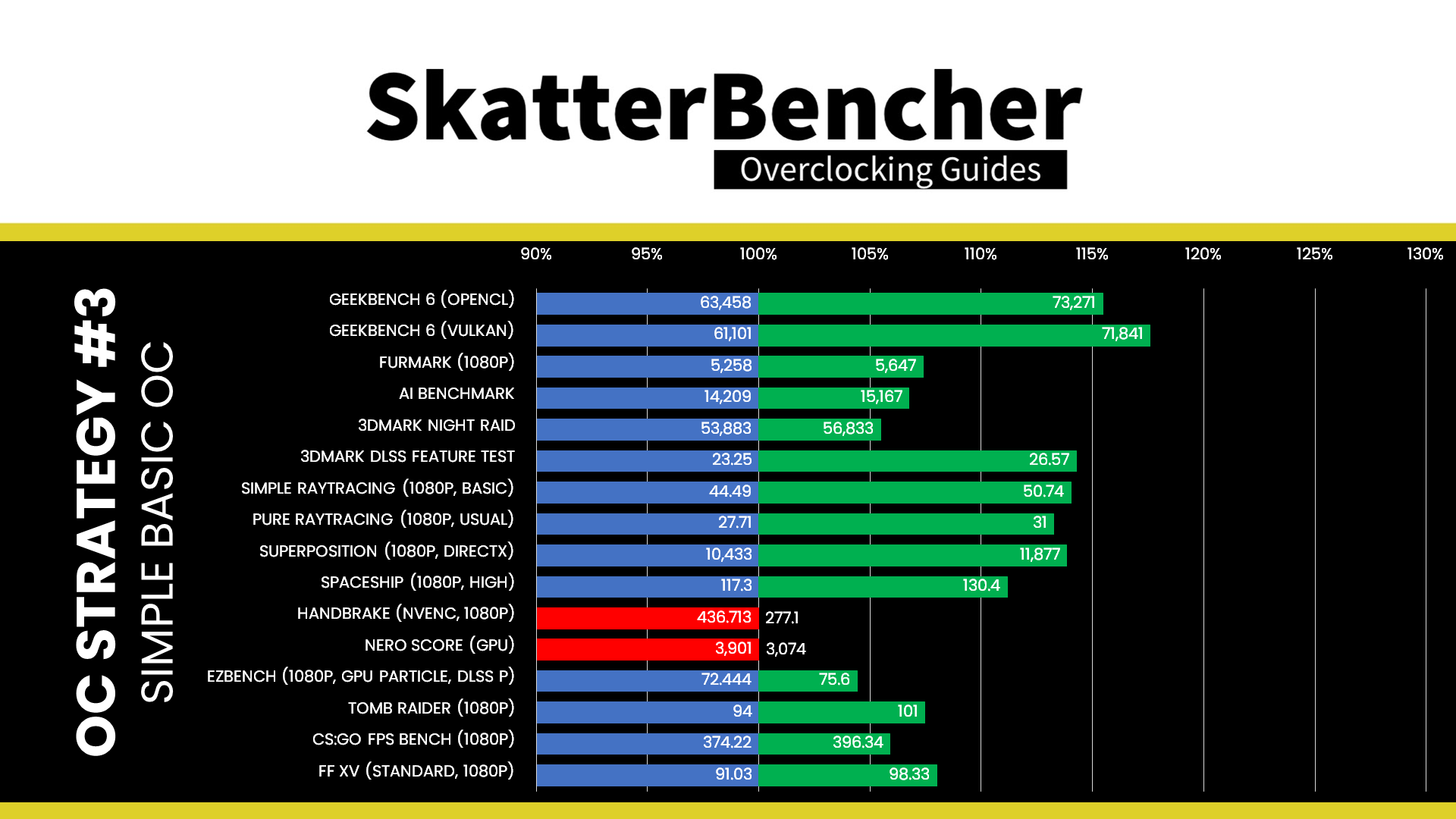
With all our additional hardware modifications, we achieve better performance than stock. However, the performance improvement is not what we’d expect. We’ll talk about what’s going on in the next segment.
When running the GPU-Z Render Test, the maximum GPU Clock is 2197 MHz with 1.254V.
When running the 3DMark Speedway Stability Test, the average GPU effective clock is 2162 MHz with 1.278 volts, and the GPU Memory clock is 2075 MHz. The average GPU and GPU Hot Spot temperatures are 53.9 and 66.8 degrees Celsius. The average GPU power is an estimated 162.416 watts.
When running the Furmark GPU Stress Test, the average GPU effective clock is 1727 MHz with 1.303 volts, and the GPU Memory clock is 2075 MHz. The average GPU and GPU Hot Spot temperatures are 58.8 and 74.9 degrees Celsius. The average GPU power is an estimated 206.530 watts.
More Performance Limitations
Now, as you may have noticed, the benchmark performance of OC Strategy #3 is not as good as OC Strategy #2 despite trying to remove more limits. Turns out that the RTX 3050 has more protection mechanisms than any of the previous NVIDIA graphics cards I’ve overclocked.


First, the good news: the hardware modifications from OC Strategy #3 effectively eliminated the voltage and power performance limiters, even in Furmark. The only remaining performance limiter is Utilization, meaning what prohibits additional performance is only the amount of CUDA cores in our GPU.

We can also check the GPU Power reporting in Furmark. We can see that the NVVDD Output Power is now much lower than before. That tells us we were right to assume this is an estimated power consumption based on the GPU VID and workload characteristics.

So, if it’s not the power limiting the performance, what’s going on? Once more, we can rely on HWiNFO to spill the beans. Let’s look at the GPU clock frequencies during the Furmark workload.

We can see two things:
- Modifying the VF curve to achieve a low VID under high loads prevents the GPU Video clock from boosting to higher frequencies. This explains the enormous performance deficit in video encoding benchmarks like Handbrake and Nero.
- As we try to increase the performance through overclocking and removing the power limitations, the GPU Effective Clock diverges further from the GPU Clock.
For reference, here’s how the GPU clock behaves during the Speedway Stress Test, which is a lighter 3D workload than Furmark.

While there’s still a delta between GPU Clock and GPU Effective Clock, it’s much less pronounced than in the heavy Furmark workload.
So, what’s going on? To be honest with you, I don’t know. At this point in my overclocking adventure, I realized I knew too little about NVIDIA’s clocking architecture to make a final conclusion. So, what follows is mostly speculation with here and there a bit of data.
What is GPU Effective Clock?
The first question we must answer is: “What is the GPU Effective Clock?”
AMD Ryzen overclockers know the term “effective clock” and how it relates to compute performance. In short, the effective clock measures the number of clock cycles within a period. In contrast, the core clock references the configured clock target. The effective clock can be lower than the core clock for various reasons, including power-saving technologies and clock stretching.

Again, AMD Ryzen CPU overclockers will be familiar with clock stretching. To keep it short, AMD employs a technology called “Voltage Adaptive Operation,” which aims to prevent system instability due to voltage fluctuations. The technology consists of two circuits: one circuit serves as a configurable voltage droop detector, and the second circuit functions as a configurable digital frequency synthesizer.

If a voltage droop is detected, the effective clock frequency is lowered to ensure continuous operation instead of a system crash. In the real world, this technology is incredibly relevant when overclocking because it may cause effective performance at a given frequency to be lower than expected.

This technology is present on AMD Ryzen CPUs as well as GPUs like the Radeon RX 6500 XT we overclocked in SkatterBencher #41. The behavior of the RTX 3050 feels similar to the clock stretching on AMD Ryzen CPUs … but not exactly like it. So, for now, let’s refer to the behavior as “GPU clock throttling” and look at some data.
Investigating GPU Effective Clock
First, we must confirm that the GPU effective clock determines the GPU performance. So, measure the performance with and without clock throttling.
In this chart, you can see the performance at a given GPU Clock when no throttling is present (blue) and when the GPU Clock is set to 2 GHZ, but there’s clock throttling (Orange). We can see that the performance is closely related to the GPU effective clock.

Next, we have to understand when GPU clock throttling occurs. So, we track the GPU effective clock during Furmark as we alter the GPU voltage.
From this chart, we can observe two important things.
- First, the GPU clock throttling appears to start when the voltage exceeds 1.1V. It may be a coincidence, but that’s also NVIDIA’s maximum operating voltage for this RTX 3050.
- Second, GPU clock throttling is much more aggressive in the heavier 1080P workload than the 720P workload.

This gives us the foundation for developing a theory about what’s happening.
It appears as if the GPU effective clock is throttled based on how much the effective voltage deviates from the maximum allowed voltage, where the maximum permitted voltage is determined by the GPU energy usage. In other words, the more energy the GPU uses, the lower the maximum allowed voltage, and the degree to which the effective GPU voltage deviates from the maximum permitted voltage determines the degree to which the GPU effective clock deviates from the GPU target Clock.

We can put that theory to the test by expanding our testing. This time, we set the GPU Clock to 2040 MHz and run Furmark across various resolutions, reflecting different load levels. We do this for three voltage levels: 1.1V (40uA, -4uA), 1.20V (50uA), and 1.30V (60uA)
Again, we can draw interesting conclusions.
- At1.3V, there’s no GPU clock throttling at the lowest Furmark Resolution however, clock throttling occurs much earlier than at lower voltage levels.
- At1.1V, there’s barely clock throttling even at the highest measured workload.

This adds further credence to our hypothesis of current-based GPU clock throttling. So, that leaves three remaining topics to discuss: (1) Why would NVIDIA implement this? (2) Did they actually implement something like this? and (3) Is there a way we can work around this?
Discussing GPU Clock Throttling
As to why NVIDIA would implement a technology that throttles the GPU clock when it detects excessive voltage based on the GPU energy use, that’s an easy question to answer: GPU health management.
All semiconductor companies implement protection mechanisms in their designs. That includes rudimentary technologies like over-temperature protection and complex technologies like voltage adaptive operation. The goal is simple: to ensure the chip operates at the warranted performance level within the warranted lifetime. Any technology that helps ensure chip lifespan is worth implementing as it can save millions of dollars at the bottom line.
NVIDIA is no different from any other semiconductor company. If it has indeed implemented a current-driven GPU clock throttling mechanism, it goes about protecting its GPUs with great care. I’m sure they never want to see anything like the media blowout of the GeForce 590 ever again.
The next question is whether NVIDIA actually implemented this kind of technology. And, to be frank, the bottom line is that we have no idea. If I had to speculate, it appears on-die voltage measurement and current estimation determine a maximum permitted voltage, and the deviation from the Vmax adjusts an adaptive clocking circuit. But NVIDIA is the only one who could shed some light on this topic.
The last question is if we can do something about it. The short answer is yes, with an XOC BIOS.
Extreme overclockers have proven the RTX 30 Ampere GPUs can go well above 1.1V with an XOC BIOS.

The XOC BIOS likely disables any power management features that govern GPU health. Unfortunately, no such XOC BIOS is available for the RTX 3050.

So, the long answer is that it’s unlikely anything we can do about it. Similar to AMD’s Precision Boost Overdrive 2 or Intel’s OC Mailbox, features that allow for manual tuning of the chip parameters must be enabled by the semiconductor company; otherwise, there’s no tuning.
I’ve talked about this issue a couple times before. Due to the increasing chip complexity and deep integration of technologies going from chip to system-on-chip, it requires increasing effort to enable chip customization. Chip customization includes overclocking to get more performance, but it’s much more than that.
Enabling silicon hyper-customization to the fullest extent means that the device owner has the means to run the chip they own at whatever voltage and frequency they choose. Whether that means running the GPU clock as high as possible for maximum performance, as low as possible to maximize power saving, or somewhere in between to maximum performance per watt.

With this RTX 3050, I feel that, despite having paid for the chip, being willing to give up any claim to warranty, and being more than willing to risk the GPU’s health, the chip manufacturer still tells me what I can and cannot do with the chip. That doesn’t feel quite right.
NVIDIA GeForce RTX 3050: Conclusion
Alright, let us wrap this up.
As I said at the beginning of the video, this has been one of the most frustrating yet interesting overclocking projects. Let me explain.
It’s been frustrating because it appears that there’s no way to work around NVIDIA’s artificial or arbitrary limitations. I understand they want to protect the GPU from unwanted damage, but I solely bought this card to experiment with. There’s no reason I shouldn’t be allowed to run the chip I own at the performance level I want. However, NVIDIA seems to disagree.
At the same time, it’s been an exciting journey because this experience made me realize I know very little about NVIDIA’s performance management technologies. So, it’s been quite fun digging into the different aspects of the performance limiters and exploring the different ways to work around the performance limiters. Of course, solving all problems and further boosting the benchmark performance would be nicer. But perhaps the real performance gained is the knowledge we absorbed along the way.
Anyway, that’s all for today!
I might look closer at another RTX 30 series graphics card in the future to see if what we learned today also applies to other GPUs. I want to thank my Patreon supporters for supporting my work. As usual, if you have any questions or comments, please drop them in the comment section below.
See you next time!