SkatterBencher #57: Intel UHD Graphics 770 (13th Gen) Overclocked to 2500 MHz
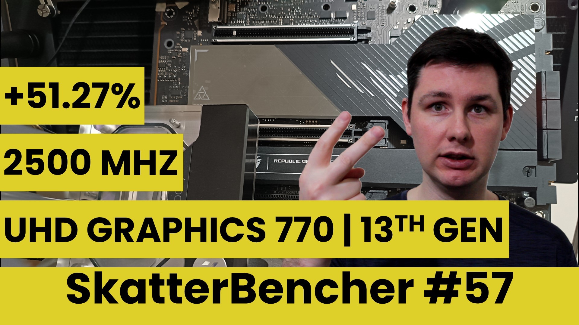
We overclock the Intel UHD Graphics 770 (13th Gen) integrated graphics up to 2500 MHz and gain up to 51% in performance using the Maximus Z790 Hero motherboard and EK-Quantum custom loop water cooling.
In my first Raptor Lake overclocking video, I hinted at a return to Intel integrated graphics overclocking. I didn’t expect to go through with it because the IP and process are identical to Alder Lake. However, when I saw the overclocking result after a quick test, I decided why not.
This SkatterBencher will be another quick guide, so strap in!
Table of Contents
Intel UHD Graphics 770 (13th Gen): Introduction
The Intel UHD Graphics 770 is the integrated graphics portion of the Intel Raptor Lake Core i9-13900K processor. It features the Intel Xe-LP microarchitecture, first introduced on 11th generation Tiger Lake and Rocket Lake.
The UHD Graphics 770 is identical to the graphics IP integrated into the Alder Lake processors; therefore, the performance and overclocking experience will be very similar too. However, since Raptor Lake sports an upgraded Intel 7 process with 3rd generation Intel SuperFin transistor, we may expect higher clock frequencies like with the P-cores.
The UHD Graphics 770 in the 13900K has 32 execution units and a maximum boost frequency of 1650 MHz, 100 MHz higher than its brother integrated into the Core i-12900K.
In today’s video, we tackle overclocking the UHD Graphics 770 (13th Gen). We will cover three overclocking strategies.
- First, we enable ASUS Multi-Core Enhancement and Intel XMP
- Second, we increase the graphics frequency to 2.1 GHz using the Graphics Ratio
- Next, we use base clock frequency overclocking to increase the graphics frequency further

However, before we jump into the overclocking, let us quickly review the hardware and benchmarks used in this blog post.
Intel UHD Graphics 770 (13th Gen): Platform Overview
The system we’re overclocking today consists of the following hardware.
| Item | SKU | Price (USD) |
| CPU | Intel Core i9-13900K | 589 |
| Motherboard | ASUS ROG Maximus Z790 Hero | 760 |
| CPU Cooling | EK-Quantum Velocity2 EK-Pro QDC Kit P360 | 137 777 |
| Fan Controller | ElmorLabs EFC-X9 | 60 |
| Memory | G.SKILL Trident Z DDR5-7800 CL36 32GB | 350 |
| Power Supply | Antec HCP 1000W Platinum | 110 |
| Storage | Kingston SSDNow SV300S37A/120 (x2) | 70 |
| Chassis | Open Benchtable V2 | 200 |
Intel UHD Graphics 770 (13th Gen): Benchmark Software
We use Windows 11 and the following benchmark applications to measure performance and ensure system stability.
Intel UHD Graphics 770 (13th Gen): Stock Performance
The first thing we must do before we start any overclocking is check the system performance at default settings.
Please note that out of the box, the ASUS ROG Maximus Z790 Hero enables ASUS MultiCore Enhancement. So, to check the performance at default settings, you must go into the BIOS and
- Go to the Extreme Tweaker menu
- Set ASUS MultiCore Enhancement to Disabled – Enforce All Limits
Then save and exit the BIOS.
Here is the benchmark performance at stock:
- Geekbench 5 OpenCL: 9,901 points
- Geekbench 5 Vulkan: 10,051 points
- Furmark 1080P: 981 points
- FluidMark 1080P: 2,133 points
- AI Benchmark: 1,379 points
- 3DMark Night Raid: 14,047 marks
- Simple RayTracing Benchmark: 22.69 fps
- Unigine Superposition: 1,870 points
- Spaceship: 16.0 fps
- Handbrake: 920.3 fps
- Nero GPU: 2,359 points
- EZBench: 249 frames
- Tomb Raider: 22 fps
- CS:GO FPS Bench: 56.10 fps
- Final Fantasy XV: 15.12 fps

When running Furmark GPU Stress Test, the average GPU Slice clock is 1650 MHz, and the average GPU Unslice clock is 1400 MHz with 1.065 volts. The average memory clock is 2400 MHz. The average GPU temperature is 45 degrees Celsius, and the average GPU power is 12.539 watts.

Now, let us try our first overclocking strategy.
However, before we get going, make sure to locate the Clear CMOS button
Pressing the Clear CMOS button will reset all your BIOS settings to default. That’s useful if you want to start your BIOS configuration from scratch. However, it does not delete any of the BIOS profiles previously saved. The Clear CMOS button is located on the rear I/O panel.

OC Strategy #1: MCE + XMP
In our first overclocking strategy, we leverage ASUS MCE and Intel XMP 3.0 technologies to enhance system performance.
ASUS MultiCore Enhancement
ASUS MultiCore Enhancement is a single BIOS option that removes all limits constraining the Intel Turbo Boost 2.0 algorithm. Effectively, it allows the CPU to run indefinitely at maximum turbo boost frequencies. On Z790 motherboards, ASUS has enabled this option by default.
Intel Turbo Boost 2.0 Technology allows the processor cores to run faster than the base operating frequency. Turbo Boost is available when the processor works below its rated power, temperature, and current specification limits. The ultimate advantage is opportunistic performance improvements in both multi-threaded and single-threaded workloads.

The turbo boost algorithm works according to a proprietary EWMA formula. That stands for Exponentially Weighted Moving Average. There are three parameters to consider: PL1, PL2, and Tau.
- Power Limit 1, or PL1, is the threshold the average power will not exceed. Historically, this has always been set equal to Intel’s advertised TDP. PL1 should not be set higher than the thermal solution cooling limits.
- Power Limit 2, or PL2, is the maximum power the processor can use for a limited amount of time.
- Tau, in seconds, is the time window for calculating the average power consumption. The CPU will reduce the CPU frequency if the average power consumed is higher than PL1.

Turbo Boost 2.0 technology is available on Raptor Lake as it’s the primary driver of performance over the base frequency.
Adjusting the power limits is strictly not considered overclocking, as we don’t change any of the CPU’s thermal, electrical, or frequency parameters. Intel provides the Turbo Boost parameters as guidance to motherboard vendors and system integrators to ensure their designs enable the base performance of the CPU. Better motherboard designs, thermal solutions, and system configurations can facilitate peak performance for longer.
Intel Extreme Memory Profile 3.0
Intel Extreme Memory Profile, or XMP, is an Intel technology that lets you automatically overclock the system memory to improve system performance. It extends the standard JEDEC specification and allows a memory vendor to program different settings onto the memory stick.
Intel Extreme Memory Profile 3.0 is the new XMP standard for DDR5 memory. It is primarily based on the XMP 2.0 standard for DDR4 but has additional functionality.

There’s a lot more to the new XMP 3.0 standard, which is outside the scope of this overclocking guide. If you’re interested in more details about XMP 3.0, check out my Alder Lake launch content.
BIOS Settings & Benchmark Results
Upon entering the BIOS
- Go to the Extreme Tweaker menu
- Set Ai Overclock Tuner to XMP I
- Set ASUS MultiCore Enhancement to Enabled – Remove All Limits
Then save and exit the BIOS.
We re-ran the benchmarks and checked the performance increase compared to the default operation.
- Geekbench 5 OpenCL: +2.06%
- Geekbench 5 Vulkan: +2.94%
- Furmark 1080P: +0.31%
- FluidMark 1080P: +0.23%
- AI Benchmark: 0.58%
- 3DMark Night Raid: +2.77%
- Simple RayTracing Benchmark: +1.98%
- Unigine Superposition: +3.85%
- Spaceship: +1.88%
- Handbrake: +9.04%
- Nero GPU: +0.08%
- EZBench: +0.80%
- Tomb Raider: +0%
- CS:GO FPS Bench: +1.69%
- Final Fantasy XV: +4.50%

Enabling XMP and unlocking the Turbo Boost 2.0 minimally impacts our benchmark performance. We see a performance increase of up to 4.5% in Final Fantasy, but we only improve by slightly over 2% on average.
When running Furmark GPU Stress Test, the average GPU Slice clock is 1650 MHz, and the average GPU Unslice clock is 1400 MHz with 1.065 volts. The average memory clock is 3900 MHz. The average GPU temperature is 45 degrees Celsius, and the average GPU power is 11.771 watts.

OC Strategy #2: MCE + XMP + GPU 2100
In our second overclocking strategy, we finally get around overclocking the integrated graphics. Just like in SkatterBencher #33 with the Alder Lake variant, it’s super simple: we just set the highest ratio in the BIOS, and everything works. To stretch out this overclocking strategy and for those who didn’t watch SkatterBencher #33, let’s spend a few minutes understanding how overclocking the integrated graphics works.
Intel UHD Graphics 770 (13th Gen): Design, Clocking, and Voltage
The term integrated graphics already reveals that the UHD Graphics 770 Xe-LP is integrated into the Raptor Lake CPU die. While the integrated graphics takes a sizeable chunk of the total die, most of the chip is used to place 8 Raptor Cove CPU P-cores and 16 Gracemont CPU E-cores, its cache, and the Ring bus.
Slice, Unslice, & Display Block
The design of the Xe-LP integrated graphics includes three parts: the “Slice,” the “Unslice,” and the display block.
- The Slice is a cluster of sub-slices, each containing elements of the actual graphics compute engine, like the execution units. It is the part that powers your games and any compute tasks.
- The Unslice holds the elements with fixed-function geometry capabilities and fixed-function media capabilities. So, if you’re encoding or decoding a video or watching Netflix, this part ensures proper video encoding. It also contains the connection to the ring bus via which the IGP can send and receive data from the system memory.
- The display block contains support for the display outputs like HDMI or DisplayPort.
The Slice part of the UHD Graphics 770 inside our desktop Raptor Lake Core i9-13900K contains two sub-slices, with each 16 execution units for a total of 32 execution units. That’s the same configuration as the Core i9-12900K. The maximum boost frequency is 1650 MHz for the Slice and 1400 MHz for the Unslice.

Clocking
When it comes to clocking, the IGP frequency is based on the base clock frequency or reference clock. By default, the BCLK is 100MHz, but it can be increased when overclocking. For the integrated graphics, the base clock frequency is first halved, then multiplied by the Graphics Ratio to obtain the final operating frequency.
Since Alder Lake, the Slice and Unslice are decoupled. That means they’re running at different frequencies. The default maximum boost frequency of the Slice is 1650 MHz, and the default maximum frequency of the Unslice is 1400 MHz. However, like on Rocket Lake, we can only control the Slice frequency using the Graphics Ratio.
On Raptor Lake CPUs, the maximum Graphics Ratio Limit is 42. That is the same as Alder Lake and Rocket Lake but lower than the previous generation Comet Lake where the maximum ratio limit was 60. Note that the display output is driven by a separate fixed clock frequency and is not affected by changing the BCLK frequency or the graphics ratio.

VccGT (GT Core Voltage)
The Raptor Lake processor has a dedicated voltage rail called VccGT or GT Core Voltage to provide an operating voltage to the graphics core.
The Slice and Unslice share the same voltage rail, so their operating voltage will be the same.
Configuring the voltage for the graphics cores is very similar to the CPU cores. Raptor Lake supports both adaptive and override voltages. When using Adaptive voltage mode, the graphics voltage will be reduced in idle. In Override voltage mode, the voltage will remain constant.

Graphics Dynamic Frequency
The Raptor Lake integrated graphics support the Graphics Dynamic Frequency feature. The Dynamic Frequency capability enables the processor power control unit (PCU) to assess its thermals, current, and power to determine a dynamic upper limit on its frequency.
On processors with Graphics Overclocking capability, the integrated graphics cores can run at higher frequencies when operating conditions allow.

When Graphics Dynamic Frequency is enabled, the graphics cores operate at any ratio in the inclusive range between the Maximum Dynamic Frequency (RP0) and the Graphics Base Frequency (RP1). In the case of our Core i9-13900K, the graphics base frequency is 300 MHz, and the default maximum dynamic frequency is 1650 MHz. We increase this Maximum Dynamic Frequency (RP0) when overclocking to a higher value.
The dynamic frequency relies on the factory-fused voltage-frequency curve for the integrated graphics to determine the appropriate voltage for a particular frequency. For this guide, I extracted the V/F curve of my specific CPU. As you can see, even though the maximum default frequency is 1650 MHz, the voltage-frequency curve scales up to 2.1 GHz.

As mentioned, the graphics frequency is partly a function of the available thermal, current, and power headroom. The Turbo Boost 2.0 technology manages that aspect of the integrated graphics. Turbo Boost 2.0 distributes the available power budget among the CPU and Graphics cores depending on the workload. So, if you have a heavy graphics-dependent workload and no CPU load, it will decrease the CPU frequency in favor of boosting the Graphics frequency higher.
Of course, knowing the power budget of the Graphics portion of the Raptor Lake CPU is only 15W means we don’t expect this power budgeting to impact our overall system performance significantly.
OC Settings & Benchmark Results
Upon entering the BIOS
- Go to the Extreme Tweaker menu
- Set Ai Overclock Tuner to XMP I
- Set ASUS MultiCore Enhancement to Enabled – Remove All Limits
- Set Max. CPU Graphics Ratio to 42
Then save and exit the BIOS.
We re-ran the benchmarks and checked the performance increase compared to the default operation.
- Geekbench 5 OpenCL: +25.28%
- Geekbench 5 Vulkan: +28.93%
- Furmark 1080P: +27.32%
- FluidMark 1080P: +27.05%
- AI Benchmark: +26.11%
- 3DMark Night Raid: +25.05%
- Simple RayTracing Benchmark: +26.71%
- Unigine Superposition: +28.34%
- Spaceship: +28.13%
- Handbrake: +8.83%
- Nero GPU: +12.34%
- EZBench: +10.04%
- Tomb Raider: +27.27%
- CS:GO FPS Bench: +29.13%
- Final Fantasy XV: +27.05%

Increasing the frequency of the UHD Graphics 770 from 1650 MHz to 2.1 GHz will improve the system’s performance. We see an average performance improvement of almost 24% and a maximum performance increase of up to 29.13% in CS:GO.
The QuickSync performance, as measured by Handbrake, remains at about +9%. That’s because the Slice and Unslice frequency is decoupled. So, by setting the Graphics Ratio, we only overclock the Slice. Since the media encoding functions like QuickSync are part of the Unslice, the performance is not impacted by the GPU overclock.
When running Furmark GPU Stress Test, the average GPU Slice clock is 2100 MHz, and the average GPU Unslice clock is 1400 MHz with 1.085 volts. The average memory clock is 3900 MHz. The average GPU temperature is 48 degrees Celsius, and the average GPU power is 15.975 watts.

OC Strategy #3: MCE + XMP + BCLK 125
In our third overclocking strategy, we rely on adjustments to the reference clock frequency to further overclock the integrated graphics. We will increase the base clock frequency to 125 MHz, and combined with a Graphics Ratio of 40, this results in a Slice frequency of 2500 MHz and an Unslice frequency of 1750 MHz.
Besides using the base clock frequency, we also increase the VccGT voltage using adaptive voltage mode. Furthermore, we also need to dig a little deeper into the clocking and voltage topology of Raptor Lake
Raptor Lake Clocking and Voltage Topology
BCLK Frequency
Raptor Lake inherits the CPU internal clock generator from Tiger Lake. The standard Raptor Lake platform has a 38.4MHz crystal as a reference clock to the PCH. The PCH then generates three clocks:
- 38.4 MHz reference clock for the CPU internal clock generator
- 100MHz PCIBCLK for PCIe, DMI, and I/O
- 24MHz frequency for TSC, display, and SVID controller
The CPU internal clock generator then generates the 100MHz base clock frequency for all the parts inside the CPU. However, Intel also offers the option to use an external clock generator. You’ll typically find this on high-end motherboards. Whichever way you get the 100 MHz BCLK, this base clock frequency is multiplied with specific ratios for each of the different parts in the CPU.
The GT frequency or graphics frequency is based on the same 100MHz BCLK but is first divided by two and then multiplied by the GT ratio. As mentioned before, the Slice and Unslice are decoupled, meaning they run at different ratios.
As you now understand, increasing the base clock frequency will impact many parts inside our CPU. So apart from adjusting the Graphics Ratio, we also need to change the default CPU ratios, Ring ratio, and DDR5 memory ratio.

CPU Turbo Ratios
Generally speaking, on Intel platforms, there are two ways to manually configure the CPU ratio: Sync all cores and by using the Turbo Ratio configuration.
Sync All Cores sets one ratio that is applied to all cores. It is very much the traditional way of overclocking.
Turbo Ratios allow us to configure the overclock for different scenarios ranging from 1 active core to all active cores. That enables a much more dynamic performance profile.
Since we are planning to increase the base clock frequency by 25%, we will adjust the default Turbo Ratio configuration to mimic the standard configuration as much as possible. For example, to achieve the maximum single-core Turbo Boost 2.0 frequency of 5800 MHz, we will set the ratio to 46X instead of 58X
VccGT Voltage Rail
On Raptor Lake CPUs, there are a total of 7 different voltage inputs.
The one relevant for overclocking the UHD Graphics 770 is called the VccGT. This voltage powers the GT or integrated graphics, including the Slice, Unslice, and Display block. You can program the graphics voltage in override and adaptive voltage mode using Intel’s overclocking toolkit.

In Override voltage mode, the voltage will remain constant, whereas using Adaptive voltage mode, the graphics voltage will dynamically change depending on the workload. When overclocking and using the adaptive mode, the CPU will interpolate the required voltage for a given frequency between the base frequency and our set maximum frequency.
You can set the adaptive voltage directly, which maps against the configured boost frequency, or you can use an adaptive voltage offset, which offsets the entire voltage-frequency curve. For example:
If our base frequency is 300 MHz at 0.9V and our maximum boost frequency is 1650 MHz at 1.05V, then the interpolated voltage for 1000 MHz will be somewhere between 0.9V and 1.05V. If the V/f curve is linear, that would be 0.98V
If we overclock our system to 2.5GHz and use an adaptive voltage offset of 300mV, the base frequency will be 300 MHz at 1.2V, and the maximum boost frequency will be 2500 MHz at 1.35V. The interpolated voltage for 1000 MHz will be somewhere between 0.9V and 1.35V. If the V/f curve is linear, that would be 1.28V.

Note that not all motherboard BIOSes expose Intel’s complete overclocking toolkit. So the configuration options may not be available. Furthermore, note that via the BIOS, we can directly program the VccGT voltage regulator to adjust the requested voltage. Any voltage offset programmed directly via the voltage regulator will increase the effective voltage but may not show up in any software tools relying on the Intel PCU data reporting.
BCLK Aware Adaptive Voltage
A crucial setting when overclocking the BCLK frequency is BCLK Aware Adaptive Voltage. This option has been on Intel CPUs since Kaby Lake back in 2016.

To understand its function, you can refer to the Adaptive Voltage Mode explanation in many of my previous Raptor Lake OC guides. Long story short, in Adaptive Voltage mode, the factory-fused voltage-frequency curve of a CPU core maps a voltage against a ratio. For example, 45X may map against 1.175V, and 52X may map against 1.35V. When the CPU boosts to a high frequency, it references the voltage-frequency curve using the configured ratio to know which voltage to apply.
When you overclock the BCLK frequency, the voltage may not be suitable for the resulting frequency.
In this specific case, we have increased the BCLK frequency to 125 MHz and have decreased the CPU ratios to match the default specification. Without enabling BCLK-aware adaptive voltage, the CPU would look up the voltage for the 45X ratio, for example, 1.175V, then use this for 5.6 GHz. That would not work out well. By enabling this setting, the CPU takes account of the adjusted base clock frequency, and the CPU will use the appropriate voltage based on the effective frequency instead of the configured ratio.

BCLK Aware Adaptive Voltage works for all V/f power domains in the CPU and produces a voltage based on frequency as opposed to the multiplier. The V/f power domains include the CPU cores, the Ring, and the integrated graphics. So it also has a significant impact on our IGP voltage frequency curve.
If we set the BCLK frequency to 125 MHz and disable BCLK Aware Adaptive Voltage, the voltage-frequency curve would look as follows. For example, we see that for 1500 MHz, the voltage would be 0.92V instead of the default 1.005V and thus may be unstable. When we enable BCLK-aware adaptive voltage, the integrated PCU will calculate the correct voltage based on the actual frequency. So, the voltage will be 1.005V again. When using BCLK-aware adaptive voltage, all frequencies below the maximum default frequency will follow the factory-fused voltage frequency curve. For the IGP of the 13900K, that’s up to 1650 MHz.

Overclock Testing
There are three other things to note when attempting to overclock the Raptor Lake integrated graphics using the BCLK.
- The limit of the Slice frequency,
- The limit of the Unslice frequency, and
- Knowing the actual GT voltage
Slice Frequency
Testing the limit of the Slice frequency is pretty straight-forward. As you increase the BCLK frequency, the Slice frequency rises accordingly. Then you can use a 3D workload to see if it’s stable. To check the actual frequency, I rely on GPU-Z Sensor information.
Unslice Frequency
Testing the limit of the Unslice frequency is similarly straight-forward. As you increase the BCLK frequency, the Unslice frequency rises accordingly. Then you can use an application like Handbrake to check the stability of QuickSync workloads. Again, I rely on GPU-Z Sensor information to check the actual frequency.
GT Voltage
Checking the current GT voltage is not as straight-forward as none of the software tools I usually rely upon seem to report the correct VccGT voltage when adjusted in BIOS. While GPU-Z reports the proper VID request from the GPU to the VccGT voltage controller, HWiNFO and XTU report an unusually low VID.
When we increase the voltage offset in the BIOS, none of the tools show an increase in voltage. That’s because the BIOS option configures the voltage offset via the voltage regulator, not Intel’s overclocking toolkit.
We can easily demonstrate this using Intel’s Extreme Tuning Utility which gives access to configuring the processor directly. If we set a +200mV offset using XTU, it also increases the reported voltage in GPU-Z. However, GPU-Z reports the default voltage if we set the same +200mV offset using the BIOS options.

So, to know what voltage we’re running at, we have to manually increase the reported voltage in GPU-Z by the configured amount in the BIOS.
In this OC strategy, we pair the 125 MHz BCLK with a Slice ratio of 40X and an offset of 0.315V. That results in a Slice frequency of 2.5 GHz and an Unslice frequency of 1750 MHz at 1.4V.

OC Settings & Benchmark Results
Upon entering the BIOS
- Go to the Extreme Tweaker menu
- Set Ai Overclock Tuner to XMP I
- Set BCLK Frequency to 125
- Set ASUS MultiCore Enhancement to Enabled – Remove All Limits
- Set DRAM Frequency to DDR5-7750MHz
- Set Performance Core Ratio to By Core Usage
- Set 1-Core Ratio Limit to 46
- Set 2-Core Ratio Limit to 46
- Set 3-Core Ratio Limit to 44
- Set 4-Core Ratio Limit to 44
- Set 5-Core Ratio Limit to 44
- Set 6-Core Ratio Limit to 44
- Set 7-Core Ratio Limit to 44
- Set 8-Core Ratio Limit to 44
- Set Efficient Core Ratio to Sync All Cores
- Set Efficient All-Core Ratio Limit to 34
- Set Max. CPU Cache Ratio to 36
- Set Max. CPU Graphics Ratio to 40
- Set BCLK Aware Adaptive Voltage to Enabled
- Set CPU Graphics Voltage to Offset Mode
- Set Offset Mode Sign to +
- Set CPU Graphics Voltage Offset to 0.315
Then save and exit the BIOS.
We re-ran the benchmarks and checked the performance increase compared to the default operation.
- Geekbench 5 OpenCL: +49.33%
- Geekbench 5 Vulkan: +50.30%
- Furmark 1080P: +51.27%
- FluidMark 1080P: +51.20%
- AI Benchmark: +50.25%
- 3DMark Night Raid: +42.78%
- Simple RayTracing Benchmark: +48.13%
- Unigine Superposition: +48.34%
- Spaceship: +50.63%
- Handbrake: +28.31%
- Nero GPU: +23.19%
- EZBench: +18.88%
- Tomb Raider: +50.00%
- CS:GO FPS Bench: +50.62%
- Final Fantasy XV: +42.99%

Thanks to the increase in base clock frequency, the integrated graphics now runs at 2500 MHz. That provides a significant performance increase over our previous overclocking strategy. We see a performance increase of up to 51.27% in Furmark 1080P. The most exciting performance increase we see in Handbrake. The rise in Unslice frequency from 1400 MHz to 1750 MHz results in a substantial improvement of the QuickSync performance measured by Handbrake.
When running Furmark GPU Stress Test, the average GPU Slice clock is 2500 MHz, and the average GPU Unslice clock is 1750 MHz with 1.400 volts. The average memory clock is 3875 MHz. The average GPU temperature is 61 degrees Celsius, and the average GPU power is 26.177 watts.

Intel UHD Graphics 770 (13th Gen): Conclusion
All right, let us wrap this up.
In my first Raptor Lake overclocking blog post, published on October 20 last year, I laid out my video plans for this Intel architecture. The plans included a SkatterBencher guide for each of the K-SKU CPUs, looking at Cryo Cooling and possibly the Raptor Lake integrated graphics if it’s interesting.
A few weeks ago, I briefly tried the Raptor Lake UHD Graphics 770 overclocking potential, and I could quickly reach 2500 MHz. That’s substantially higher than we could do with the same IP in Alder Lake. So, a separate video was a must. However, despite the improved overclocking capability, the overclocking process is identical to Alder Lake, and it still doesn’t turn the IGP into an incredible gaming chip.
With this video, I conclude my Raptor Lake testing. I covered each K variant (13900KS, 13900K, 13700K, and 13600K), the benefits of Cryo Cooling, and the integrated graphics. Unless something spectacular pops up soon, it’s time to move on to other platforms.
Anyway, that’s all for today!
I want to thank my Patreon supporters for supporting my work. If you have any questions or comments, please drop them in the comment section below.
See you next time!

Intel UHD Graphics 770 - Testamos como anda o vídeo integrado da Intel! - The Overclock Page
[…] Dito isso, foi possível atingir 2219 MHz no iGPU com tensão fixada em 1.35V, o que parece razoável, contudo, existem relatos de exemplares de 13ª geração chegando aos 2500 MHz. […]
Dante
Hi
Thank you for the article.
I want to know what is the maximum safe voltage for VccGT (GT Core Voltage)?
Pieter
According to Intel documentation the maximum spec is 1.5V, however for daily use I’d stick with 1.35V or so. Usually there isn’t much scaling beyond that anyway
5 Minute Overclock: Intel UHD Graphics 770 (Raptor Lake) to 2500 MHz - 5 Minute Overclock
[…] I’ll speedrun you through the BIOS settings and provide some notes and tips along the way. Please note that this is for entertainment purposes only and most certainly not the whole picture. Please don’t outright copy these settings and apply them to your system. If you want to learn how to overclock this system, please check out the longer SkatterBencher article. […]