Raphael Overclocking: What’s New
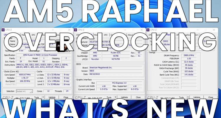
Raphael is finally here and just like with every new generation, a new CPU means new overclocking features.
AMD’s brand new AM5 platform features the Raphael desktop processors and the Zen 4 architecture. AM5 is AMD’s first new socket for mainstream desktops since 2016 and coincides with the transition to DDR5 memory.
Just like with every new CPU, there are new overclocking features.
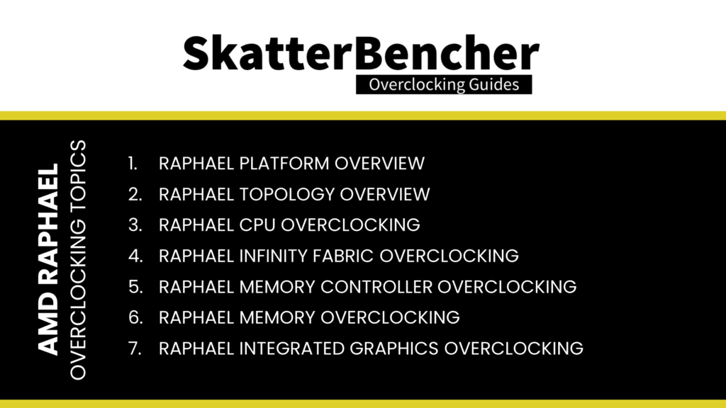
In this article, we’ll dig into everything new about overclocking AM5 processors like Raphael. We’ll dig into the following topics:
- Review the AM5 platform, including the Raphael process, architecture, SKUs, and chipsets.
- General look at the CPU Clocking and Voltage topology
- CPU core overclocking,
- Infinity fabric overclocking
- Memory controller overclocking
- DDR5 memory overclocking,
- Integrated graphics overclocking.
After covering the theoretical side of overclocking, we’ll also cover Raphael overclocking from the practical perspective.
- ASUS Crosshair X670E Gene overclocking tools
- Raphael overclocking expectations for both ambient and extreme cooling
- Practical example of the AMD Raphael overclocking approach and BIOS configuration.

This blog post is mainly targeted at people who are not very familiar with AMD CPUs yet and want to have a more detailed introduction to the ins and outs of performance tuning. But hopefully, it will also provide some information for the more seasoned Ryzen overclockers out there.
Alright, we have lots to cover, so let’s get started.
AMD Raphael Platform Overview
AMD Raphael is the codename for the Ryzen 7000 series mainstream desktop processors. It is the successor to Vermeer Zen 3 Ryzen 5000, features the Zen 4 CPU micro-architecture, and the brand-new AM5 socket.
AMD Raphael Process
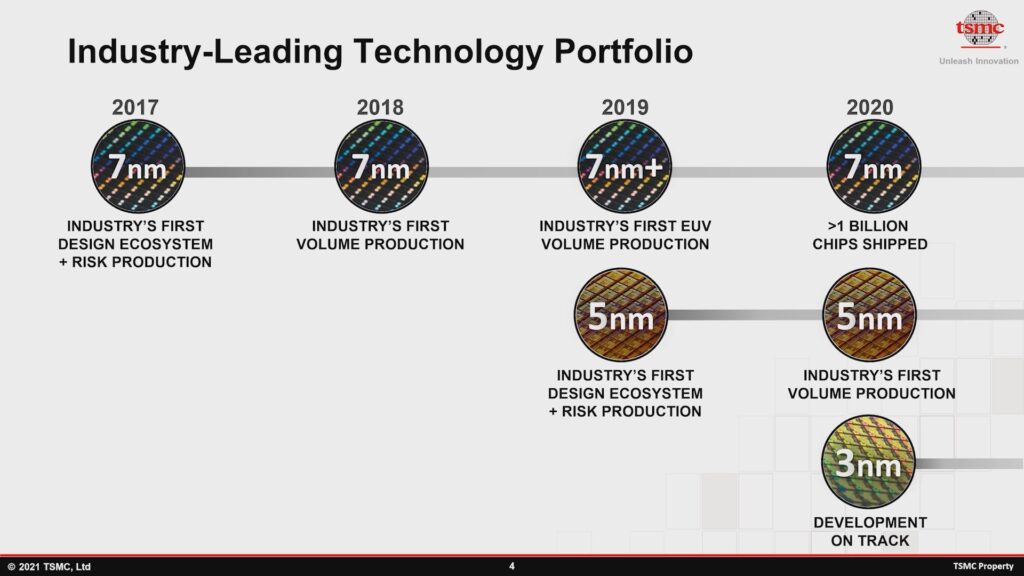
Zen 4 is AMD’s first core fabricated using a modified version of TSMC’s 5nm process. TSMC’s N5 node is their second-generation lithography with EUV technology.
Going from N7 to N5 offers several benefits, including potential increases in the operating frequency, reduced power consumption, and increased logic density. Increased logic density can be utilized in various ways. For example, making smaller (and thus cheaper) chips, adding more functionality like AVX-512, or optimizing the chip layout to achieve higher frequency.
TSMC N5 has enabled AMD to make significant strides in achieving higher frequencies for its 8-core Zen 4 CCD and increasing core density with its 16-core Zen 4c CCD.
AMD Raphael Architecture
I won’t cover the architecture in detail as plenty of media have and will cover this in detail. What’s important to know is that the CPU package is similar to previous generations of Ryzen processors.
Depending on the specific SKU, you’ll find two or three chips on the CPU package: one or two CCDs and one IOD.
- CCD stands for Core Complex Die and is simply a chip with the Zen CCX and infinity fabric connections.
- CCX stands for Core Complex and contains up to 8 Zen 4 cores, each with their own L1 and L2 cache and a shared L3 cache.
- IOD stands for I/O Die and includes all the IO connectivity, including the DDR5 memory controllers.
Note that while the CCDs are fabricated on TSMC 5nm, the IO Die is fabricated using TSMC 6nm.

Key architectural differences between Zen 3 and Zen 4 include:
- Support for AVX-512 instructions to enable AI acceleration
- Increased cache size
- Increase overall clock speeds
- Support for DDR5 memory
- Support for PCIe 5.0.
Overall, architecturally, Zen 4 is more of an evolution than a revolution compared to Zen 3.
It is worth mentioning that Zen 4 has 2 derivative products: Zen 4 with 3D V-Cache and Zen 4c.
The Zen 4 with 3D V-Cache is, as the name implies, a Zen 4 CCD with a layer of additional 3D V-Cache on top. AMD first launched such products with Zen 3 in the form of the Ryzen 7 5800X3D for consumers and Milan-X for the data center. The additional 3D V-Cache greatly expands the available shared L3 cache on a given CCD. It is expected that Zen 4 with 3D V-Cache will be announced beginning next year.
The Zen 4c is a new product designed for cloud-native compute leadership in the data center. At the moment of writing, not much is known about Zen 4c other than it has ISA-parity with Zen 4 but sacrifices L3 cache size for additional CPU cores. Zen 4c is expected to launch later this year as part of the Zen 4 EPYC product line.
We can speculate that Zen 4c CCD features 2 CCXs with each 8 Zen 4 cores based on AMD’s 128-core EPYC “Bergamo” announcement. That aligns with AMD’s claim that going from TSMC N7 to N5 offers 2x density improvement.
What may not be obvious is that there should be nothing preventing AMD from adopting Zen 4c on mainstream platforms. Thus, it may open the door for 8+16 or even 16+16 core designs on AM5.

AMD Raphael Processors
The Ryzen desktop processors come in three flavors: Ryzen 9, Ryzen 7, and Ryzen 5. So far we’ve only learned about the -X variants. But, it’s reasonable to assume we’ll also see non-X lower power variants in the future.
The SKUs available at launch are the 16-core Ryzen 9 7950X, 12-core Ryzen 9 7900X, 8-core Ryzen 7 7700X, and 6-core Ryzen 5 7600X.
The Ryzen 9 7950X processor has 2 CCDs with 8 Zen 4 cores each, totaling 16 cores and 32 threads. The base frequency is 4.5 GHz. The advertised Precision Boost 2 boost frequency is 5.7 GHz. The processor TDP is 170W, and PPT is 230W.
The Ryzen 9 7900X processor has 2 CCDs with 6 Zen 4 cores each, totaling 12 cores and 24 threads. The base frequency is 4.7 GHz. The advertised Precision Boost 2 boost frequency is 5.6 GHz. The processor TDP is 170W, and PPT is 230W.
The Ryzen 7 7700X processor has 1 CCD with 8 Zen 4 cores each, totaling 8 and 16 threads. The base frequency is 4.5 GHz. The advertised Precision Boost 2 boost frequency is 5.5 GHz. The processor TDP is 105W, and PPT is 142W.
The Ryzen 5 7600X processor has 1 CCD with 6 Zen 4 cores each, totaling 6 cores and 12 threads. The base frequency is 4.7 GHz. The advertised Precision Boost 2 boost frequency is 5.3 GHz. The processor TDP is 105W, and PPT is 142W.

The default Precision Boost 2 algorithm parameter limits can be found in the table below.

Totally new for AMD CPUs is the integrated graphics. The only purpose of the integrated graphics is as a display controller and basic media decoder. It’s most definitely not intended to be used for gaming.
The integrated graphics included in Raphael CPUs is branded as AMD Radeon Graphics and carries the GFX1036 ID. It features the RDNA 2 architecture and is part of the Navi 2 product family. The integrated graphics has 2 Compute Units with 128 stream processors and 1 ray accelerator. That makes it 6x lower spec than the Radeon RX 6400. The base clock frequency is 600 MHz, and the boost frequency under load is 2200 MHz.

AMD Raphael CPUs fit the AM5 LGA1718 socket and will work on AMD 600 series motherboards. Like its predecessor, AM5 is expected to have a long lifecycle spanning multiple generations of Zen processors.
AMD Raphael Chipsets
With new CPUs that fit new sockets come new motherboards with new chipsets. While I won’t cover the chipset features in-depth, a brief overview is never a bad thing.
Unlike the X570 chipset, which was designed by AMD, the 600 series chipsets are entirely outsourced to ASMedia. There are 3 configurations expected for the 600-series chipset known as Promontory 21:
- High-end X670
- Mid-end B650
- Low-end A620
The main difference is that X670 features 2 daisy-chained B650 chipsets, and the A620 is a defeatured B650 chipset. There are -E variants of both X670 and B650. The difference between -E and non-E is that motherboards with the -E designation are required to support PCI-e 5.0 for both primary PCIe and M.2 slots.

In terms of performance, you may expect a potential bandwidth bottleneck on X670 when all lanes are in use. That’s because the secondary chipset data first passes through the PCIe 4.0 x4 lane to the primary chipset, with its own IO, then again passes through a PCIe 4.0 x4 link to eventually end up at the CPU.
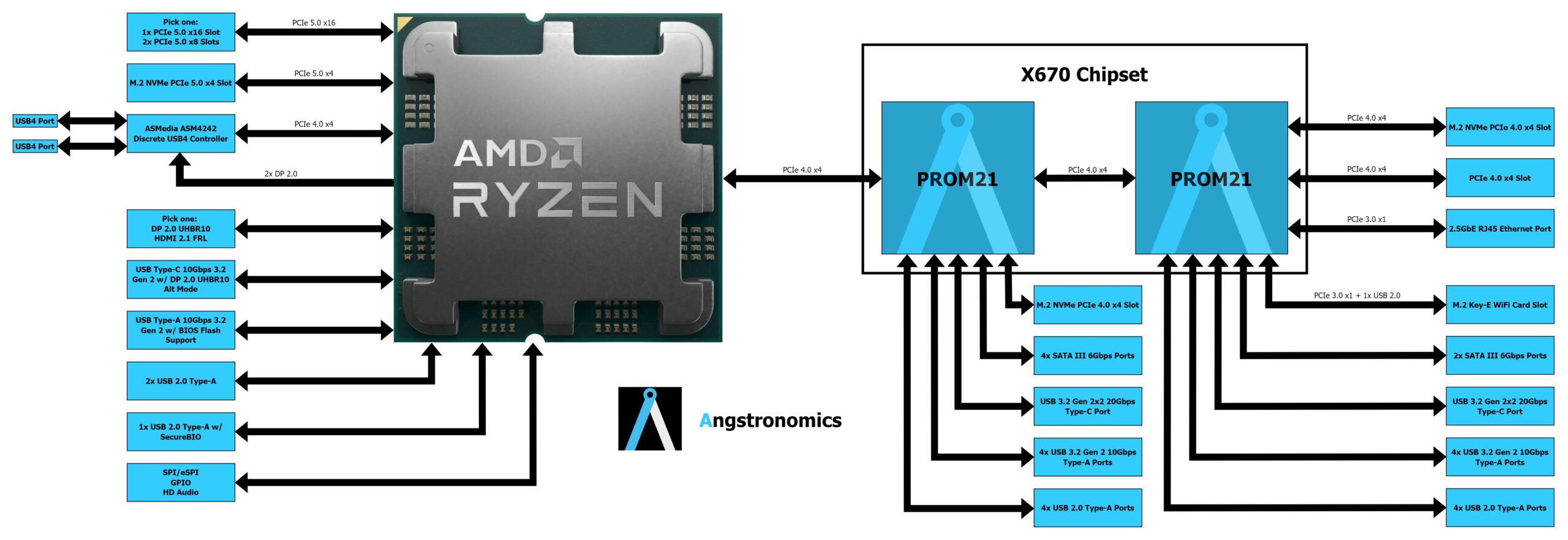
Both the X- and B-series chipsets enable support for overclocking. In contrast, the A-series is expected not to support any overclocking.
AMD Raphael Topology
Before we get to the overclocking, let’s first look at the Raphael Topology for both the clocking and voltage.
AMD Raphael Clocking Topology
The clocking of AMD Raphael is similar to the previous generation of Zen 3 Vermeer desktop CPUs.

The standard Raphael platform has a 48 MHz crystal input to the integrated CGPLL clock generator. The CGPLL then generates a 48 MHz clock for the USB PLL and a 100 MHz reference clock for the FCH, which contains the CCLK PLL for the CPU cores and several SOC PLLs.
The CCLK PLL 100MHz reference clock drives the 200 MHz VCO, which is then multiplied by an FID and divided by a DID. As a whole, this provides CPU clock frequency granularity of 25 MHz.
As with Vermeer, each CCX has its own PLL, with the cores within that CCX running at the same frequency..
The SOC PLLs include a wide range of PLLs present on the IO die. The ones most relevant for overclocking are:
- FCLK for the data fabric
- UCLK for the memory controller
- MCLK for the system memory
- GFXCLK for the integrated graphics
Unlike Zen 3, the memory controller, system memory, and data fabric run no longer at the same frequency by default. That’s because DDR5 memory can run at much higher frequencies than DDR4, while the fabric clock can’t.
- FCLK is the term used for the infinity fabric clock frequency. It is, by default, 1733 MHz but can be set to 3000 MHz using the available frequency options.
- UCLK is the term used for the unified memory controller clock frequency. It runs by default at the same frequency as the system memory, though motherboard auto-rules may drop it to half the frequency if system memory exceeds DDR5-5800. It is relatively inflexible as it can run either at the same or half the system memory frequency. It can be overclocked to 6000 MHz using the available frequency options.
- MCLK is the term used for the system memory clock frequency. It is by default either the same or double the memory controller frequency. It can be overclocked to DDR5-12000 using the available memory ratio options
- GFXCLK is the term used for the integrated graphics core clock frequency. At stock, it will go up to 2.2 GHz during a 3D load. It can currently not be overclocked.
What’s new on Raphael is the return of eCLK mode. ECLK stands for external clock and is precisely what the term suggests: an external clock generator. It was previously available on Ryzen 2000 Pinnacle Ridge processors but was removed afterward.
In addition to the standard internal CGPLL, Raphael supports up to two external clock modes. They’re called eCLK0 Mode and eCLK1 Mode.
In eCLK0 Mode, also referred to as synchronous mode, an external 100MHz reference clock is used for both the CPU PLL and SOC PLLs. In other words, it’s a reference clock that affects the CPU core clocks as well as the PCIe and SATA clocks. The USB PLL is still driven by the 48 MHz crystal via the CGPLL.

In eCLK1 Mode, also referred to as asynchronous mode, there are two distinct external 100MHz reference clocks. One clock provides the 100MHz input for the CPU PLL, and another provides the 100MHz reference clock for the SOC PLLs. AMD suggests up to 140 MHz can be expected for the CPU core reference clock, but your mileage may vary. The USB PLL is still driven by the 48 MHz crystal via the CGPLL.

AMD Raphael Voltage Topology
From the voltage topology perspective, there are a few minor changes. Like Vermeer, the processor still relies on an internal and external power supply to generate the processor voltages.
There are four primary power supplies from the motherboard VRM to the processor: VDDCR, VDDCR_SOC, VDDCR_MISC, and VDDIO_MEM_S3.

The VDDCR voltage rail provides the external power for two internal voltage regulators: VDDCR_CPU and VDDCR_VDDM.
VDDCR_CPU provides the voltage for the CPU cores within the CCX. On CPUs with multiple CCXs, each CCX has its own VDDCR_CPU voltage rail, but the voltage will be identical. The voltage rails can work in either regular or bypass mode, but on Raphael, it is always in bypass mode. That means the voltage is always equal to the VDDCR external voltage.
VDDCR_VDDM provides the voltage for the L2, L3, and, if present, 3D V-Cache on a CCX. On CPUs where there are multiple CCXs, each CCX has its own VDDCR_VDDM voltage rail. This rail cannot work in bypass mode; therefore, it is always internally regulated from the VDDCR external voltage rail. The default VDDM voltage is 0.95V
A quick word on bypass mode. As with previous platforms, AMD extensively uses fully digital integrated voltage regulators. The voltage regulators are ultra-high efficiency digital low-dropout or dLDO. Most of the power domains, including the CPU cores, caches, fabric, and so on, have dLDOs that can be controlled individually. However, most of these dLDOs are permanently bypassed on consumer parts like Raphael. That means the regulators are disabled, and the voltage regulation takes place on the motherboard via the VRM. A prime example is the voltage for the CPU cores.

The dLDOs for the CPU cores are still present on the CCDs, just like on the Ryzen 5000 series processors. However, they cannot be enabled by the end user. But we can still show you how it would work using specialized tools.
We can illustrate the behavior by using a single-threaded application like SuperPI 32M.
For stability reasons, I have to set the Fmax to 4550 MHz and the Curve Optimizer to +30. Then I log the system information using HWiNFO.
Now, if we run SuperPI 32M assigned to Core 1 and check the per Core VIDs, we find that they’re pretty much the same around 1124mV. That’s pretty much the same as the VDDCR_CPU voltage rail. That makes sense, as disabling dLDO means we put it in bypass mode and power all CPU cores directly from the VDDCR_CPU voltage rail.


When we use a specialized tool to enable dLDO and run the same test, we find that the Core VIDs for each core are now totally independent. The core running SuperPI 32M is running at 1100mV, whereas the other cores are running at a lower voltage between 1085mV and 1115mV. The VDDCR_CPU voltage rail is still at 1126mV.


If we look at the power consumption, we find that Core 1 consumes 4.27W in bypass mode and 4.15W in dLDO mode. That’s a difference of 3%. When we look at the rest of the Cores in the first CCD0, we find that the average power used in idle is 0.19W in bypass mode and 0.15W in dLDO mode. That’s a difference of 21%. The cores in the second CCD idle at only 0.04W in bypass mode and 0.03W in dLDO mode. That’s a difference of 16%.

Unfortunately, it seems impossible to run dLDO mode when the core voltage is higher than 1.25V.
The VDDCR voltage rail can be directly controlled via the SVI3 interface. VDDCR_VDDM cannot be controlled by the end-user
The VDDCR_SOC voltage rail provides the external power for multiple internal voltage regulators on SOC for the various IP blocks, including but not limited to the memory controller, SMU, PSP, graphics, etc. It is essential to know that the VDDCR_SOC voltage must always be lower than VDDIO_MEM_S3 + 100mV. The default VDDCR_SOC voltage is 1.05V.
VDDCR_GFX provides the voltage for the GPU cores on the IO die. The voltage rails can work in either regular mode or bypass mode. In regular mode, the voltage is managed by the integrated voltage regulator and derived from the VDDCR_SOC voltage rail. When the integrated VR is disabled in bypass mode, and the voltage is equal to the VDDCR_SOC voltage rail.
The VDDCR_SOC voltage rail can directly be controlled via the SVI3 interface.
The VDDCR_MISC voltage rail provides the external power for the internally regulated VDDG voltage rail. VDDG is the voltage supply for the infinity fabric data path. There are a total of 4 independently configurable VDDG voltages: CCD0-CCD, CCD0-IOD, CCD1-CCD, and CCD1-IOD. Each represents a specific GMI link connection
- CCD0-CCD VDDG: signals sent from CCD0 to IOD are sent at this voltage
- CCD0-IOD VDDG: signals sent from IOD to CCD0 are sent at this voltage
- CCD1-CCD VDDG: signals sent from CCD1 to IOD are sent at this voltage
- CCD0-IOD VDDG: signals sent from IOD to CCD1 are sent at this voltage
When overclocking your DDR5 memory, you may need to manually increase the VDDG voltage as it does not automatically adjust when changing the VDDCR_MISC voltage.
The VDDCR_MISC voltage rail can be directly controlled via the SVI3 interface. In contrast, the VDDG voltages can only be configured using the CPU registers. The default VDDCR_MISC voltage is 1.1V, and the default VDDG voltage is 0.85V
The VDDIO_MEM_S3 voltage rail provides the external power for the VDDP_DDR internal voltage regulator. VDDP is the voltage for the DRAM PHY. As a rule, VDDIO_MEM_S3 should always be higher than VDDP_DDR + 100mV. When memory overclocking, you may need to manually increase the VDDP voltage as it does not automatically adjust when changing the VDDIO_MEM_S3 voltage. The default VDDIO_MEM_S3 voltage is 1.1V. The default VDDP voltage is 0.8V.
AMD Serial VID Interface 3 (SVI3)
AM5 Raphael CPUs support the new AMD SVI3 standard. SVI stands for Serial VID Interface and is an AMD-designed VR controller interface.
AMD introduced the 1st generation SVI to NDA partners in January 2006 as the successor to its PVI technology. It was introduced to the market with Socket AM2+ processors about one year later.
The main advantage of SVI is that it provides an I2C-compliant interface between the CPU and VR controller. I2C requires only 3 connections for data (SDA), clock (SCL), and ground (GND). This removes the need for increasing the number of parallel connections between the voltage regulator and CPU to support additional features.
The 2nd generation SVI was available to NDA partners in February 2010 and provides a range of features, including greater granularity in voltage selection, faster data rate, and telemetry functions. It was introduced to the market with Socket FM2 Trinity processors in 2012.

The 3rd generation SVI was available to NDA partners in November 2018 and was first implemented on the 2022 Ryzen 6000 Rembrandt mobile APUs and is now also available on AM5 Raphael.
The Serial VID Interface Version 3 is designed to provide a scalable single-master, multi-slave communication bus for power management on AMD platforms. SVI3 represents a significant deviation from SVI2 and all previous AMD power management interfaces.
Similarities include:
- Single-master interface
- 3-wire push-pull signaling (from the master)
- Dedicated telemetry bus
Major differences include (but are not limited to):
- Multi-slave interface supporting up to 63 devices with explicit addressing
- Daisy-chain telemetry topology
- Direct register read/write functionality
SVI3 is not designed to be backward compatible with SVI2, so it is not required for SVI3 devices to function on an SVI2 bus. However, advanced slave devices may include the ability to work in SVI2 mode.
AMD Precision Boost 2
Precision Boost 2 is an automatic performance-maximizing technology available in all AMD Ryzen processors since the 2018 Ryzen 2000 series. This technology improves system performance by dynamically increasing your processor clock speeds.
Precision Boost 2 behavior depends on several factors, including temperature, power consumption, current draw, and the number of active cores.

We don’t have up-to-date information on exactly how the Precision Boost 2 algorithm works with Zen 4 Ryzen 7000 CPUs. However, AMD detailed how Precision Boost worked on the first-generation Zen in a 2018 paper titled “Zeppelin”: An SoC for Multichip Architectures. We can assume that the technology still essentially works in the same way.

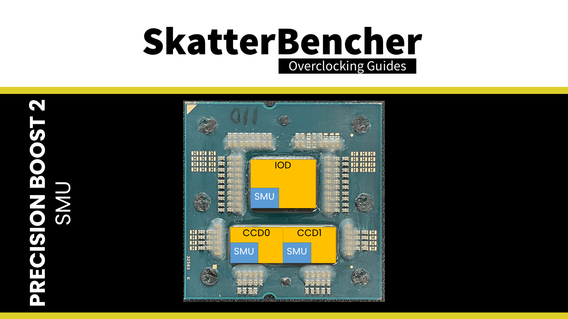
SMU – System Management Unit
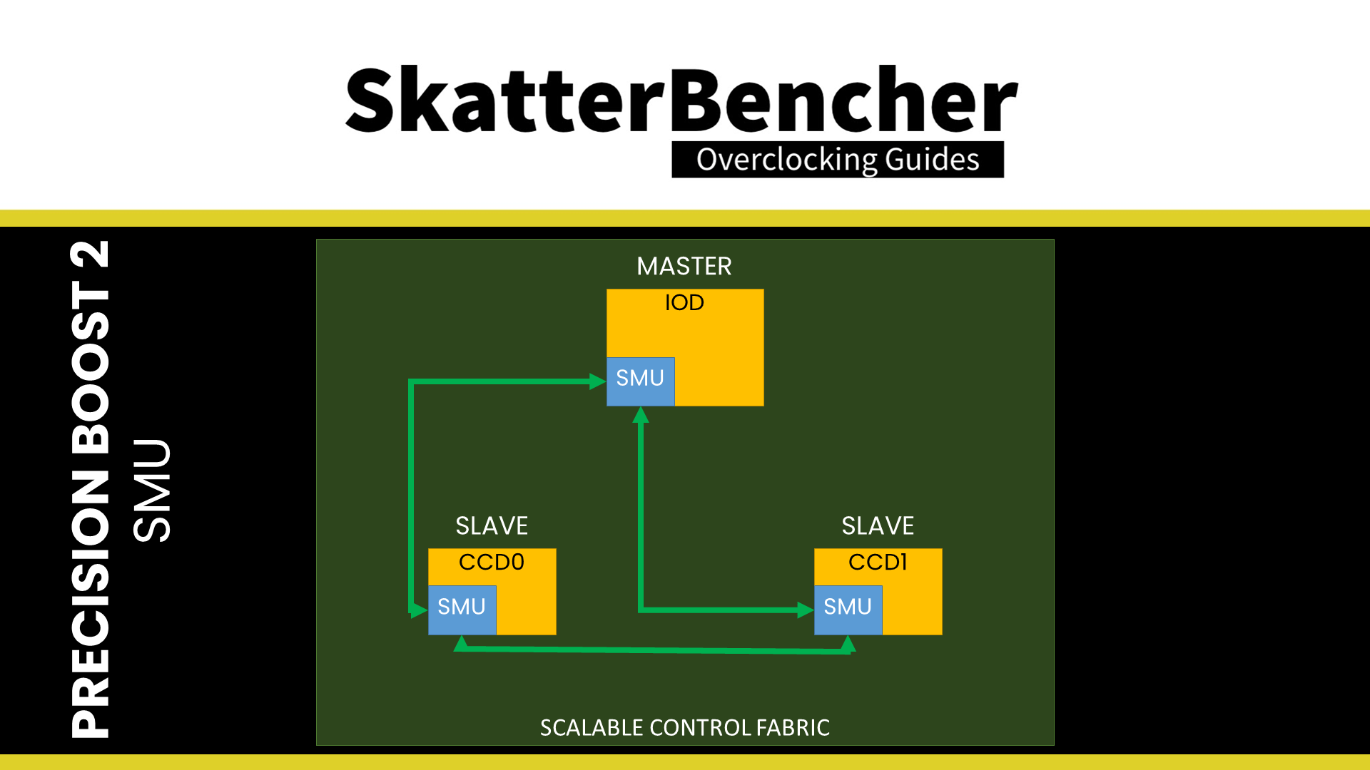
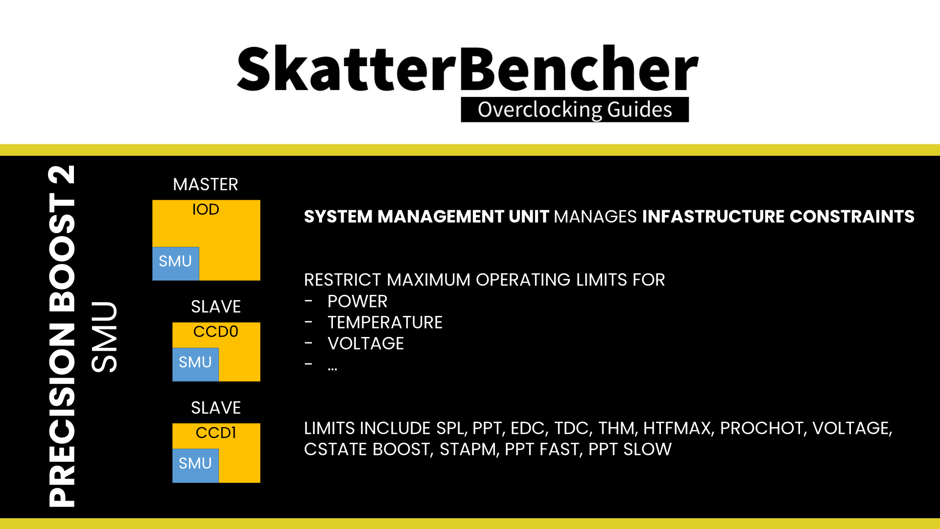
The Precision Boost magic is performed by the SMU. SMU is short for System Management Unit. Each chip on your Raphael CPU has an SMU, meaning there are 3 SMUs on a Raphael CPU with 2 CCDs and 1 IOD. One of those SMUs will work as Master SMU, while the others work as Slave SMUs. Typically, the SMU in the IO die would be the Master SMU. All SMUs are connected using a low-bandwidth control bus called SCF or Scalable Control Fabric.
The SMU has a range of capabilities, including, most importantly, the ability to manage the CPU performance within the infrastructure constraints. The infrastructure restricts the maximum operating limits on various metrics, including power draw, temperature, and voltage. We don’t have a comprehensive, confirmed list of metrics, though some are exposed to the end-user. On Raphael, the exposed infrastructure limits include the following: SPL, PPT, EDC, TDC, THM, HTFMax, ProcHot, Voltage, CState Boost, STAPM, PPT Fast, and PPT Slow. We’ll have a closer look at each of these in a minute.
The primary function of the slave SMUs is to capture the measurement data related to the infrastructure limits, then prepare that data to be sent to the master SMU. The master SMU’s primary function is to analyze the package-wide measurement data and determine the actions needed for performance management.
Each infrastructure limit has its own algorithm and is managed independently by the master SMU to determine the infrastructure limited frequency. The process for each algorithm is as follows:
- Receive data from the slave SMUs
- Aggregate the data into a single evaluation, with the output being the maximum frequency limit for a given infrastructure algorithm
- Input the result to a PID (proportional-integral-differential) controller, which smoothens out the responses over a longer period and avoids spikes or quick changes
- The changing output of the PID controller is the maximum frequency allowed by a specific infrastructure limit at a given time.
This process is repeated approximately every 1 millisecond for each algorithm.
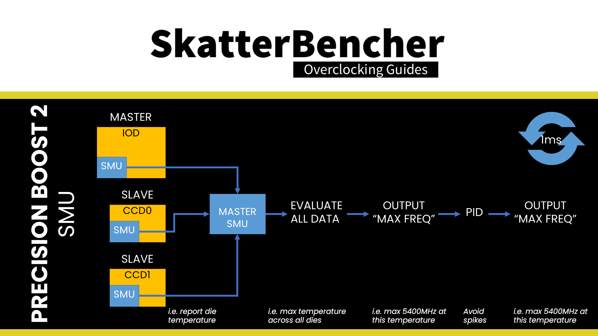
The firmware then selects the most constraining limit as the global frequency limit.
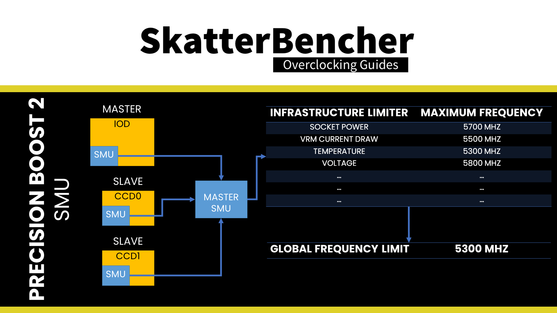
Then, either of two things can happen: the current frequency exceeds the limit, or it doesn’t. If it does, the frequency is reduced. If it doesn’t, there’s frequency headroom, and the frequency will increase.
Either way, the master SMU passes the frequency change request to the slave, and each slave applies the frequency changes to the CPU cores of the local die. The frequency changes are coordinated with the global voltage plane by the master SMU.
If the frequency increases, the master first sends a VID voltage command to the external voltage regulator before sending frequency increase commands to the slave SMUs.
If the frequency decreases, the master first sends the frequency change request to the slaves. Then it waits for the frequency change to be acknowledged. Lastly, it sends the VID voltage command to the voltage regulator.
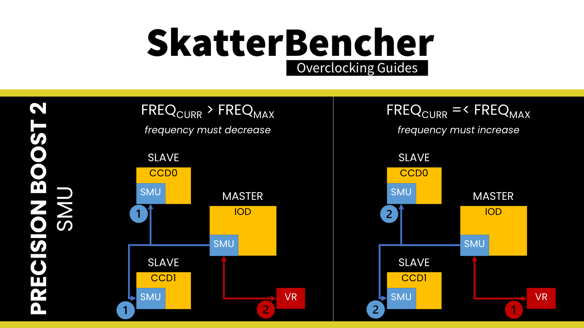
The slave SMUs can make independent decisions based on local conditions. So, it can apply lower frequencies than the frequency requested by the master SMU if the on-die conditions require so. For example, one CCX may run a lower frequency in all-core workloads than the other. Additionally, when dLDO is enabled, each SMU can independently adjust the voltage for each core within the CCX.
Precision Boost Infrastructure Limiters
Now, let’s have a closer look at the Precision Boost infrastructure limiters exposed to the end-user. While all these limiters are present on a Ryzen 7000 CPU, it doesn’t mean they’re all active or configured. Some limiters are not relevant to a desktop system and may be ignored.
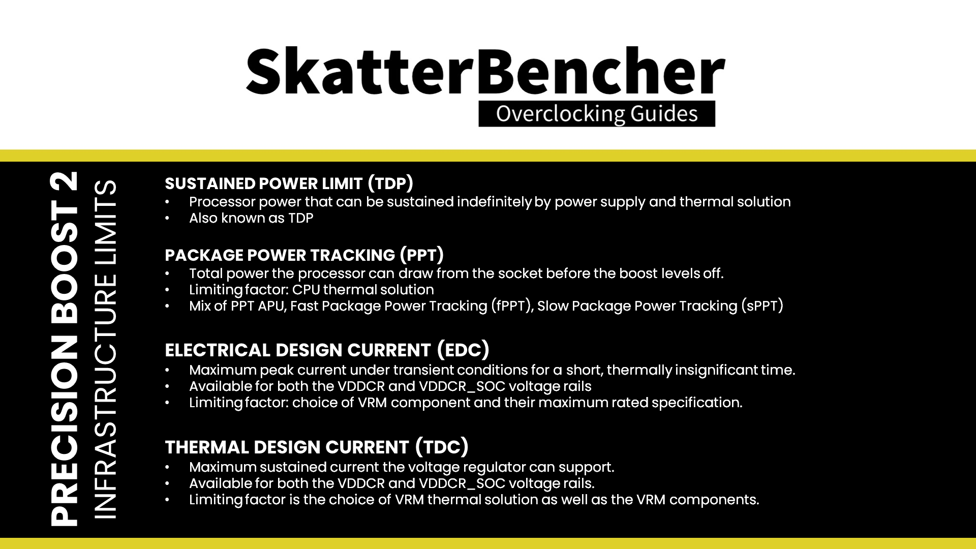
Sustained Power Limit, or SPL, is the processor power that can be sustained indefinitely by the power supply and thermal solution. It’s also known as the TDP.
Package Power Tracking, or PPT, is the total power the processor can draw from the socket before the boost levels off. Typically, the limiting factor is your CPU thermal solution.
In technical documentation, you’ll find that PPT is actually a combination of three power-related options: PPT APU (PPT), Fast Package Power Tracking (fPPT), and Slow Package Power Tracking (sPPT). Depending on your platform, some of these parameters may not be used. For desktop Raphael, Fast PPT is the parameter we override when configuring PPT.
Electrical Design Current, or EDC, represents the maximum peak current the voltage rail can demand under transient conditions for a short, thermally insignificant time. Independent EDC tuning is available for both the VDDCR and VDDCR_SOC voltage rails. Typically, the limiting factor is the choice of VRM components and their maximum rated specification.
Thermal Design Current, or TDC, represents the maximum sustained current the voltage regulator can support. Independent TDC tuning is available for both the VDDCR and VDDCR_SOC voltage rails. Typically, the limiting factor is the choice of VRM thermal solution and the VRM components.
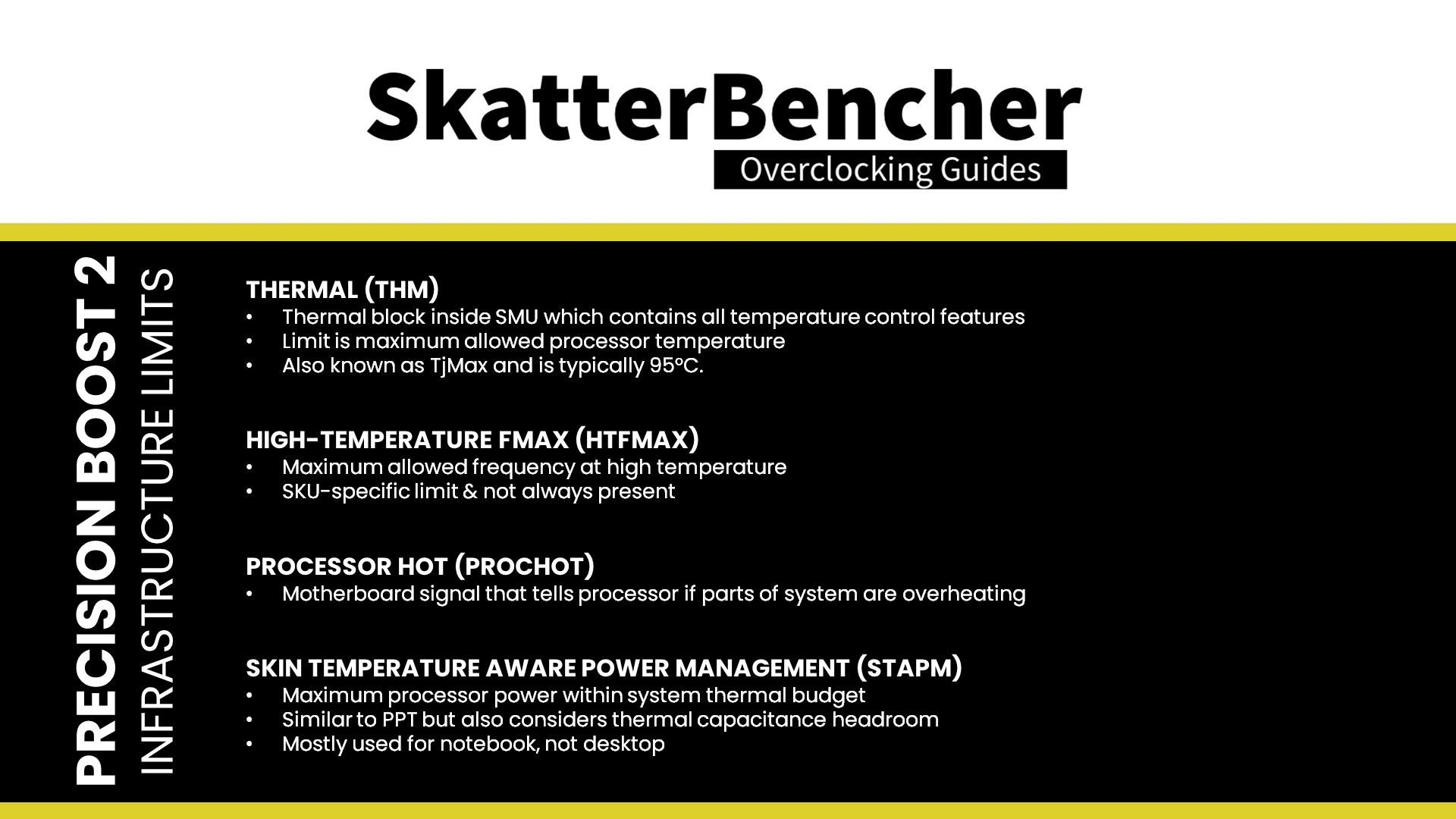
Thermal, or THM, represents the thermal block inside the SMU that contains all temperature sensors, control, and reporting features. The THM limit is the maximum allowed processor operating temperature and is commonly known as TjMax.
High-temperature Fmax, or HTFMax, represents the maximum frequency allowed at high operating temperatures. This limiter is SKU-specific and may or may not be present. For example, on the 7600X, the HTFmax limiter starts at 5450 MHz at 70 degrees Celsius. The frequency reduces linearly until it reaches 5150 MHz at 95 degrees Celsius. However, on the 7900X, this limiter does not appear to be present.
Processor Hot, or PROCHOT, is a signal within the motherboard design that tells the processor other system elements are overheating and allows the processor to throttle performance.
Skin Temperature Aware Power Management, or STAPM, represents the maximum power the processor can use within the thermal budget of the whole system. It is similar to the package power but also considers the system thermal capacitance headroom. It is primarily relevant for notebooks, not so much for desktop.
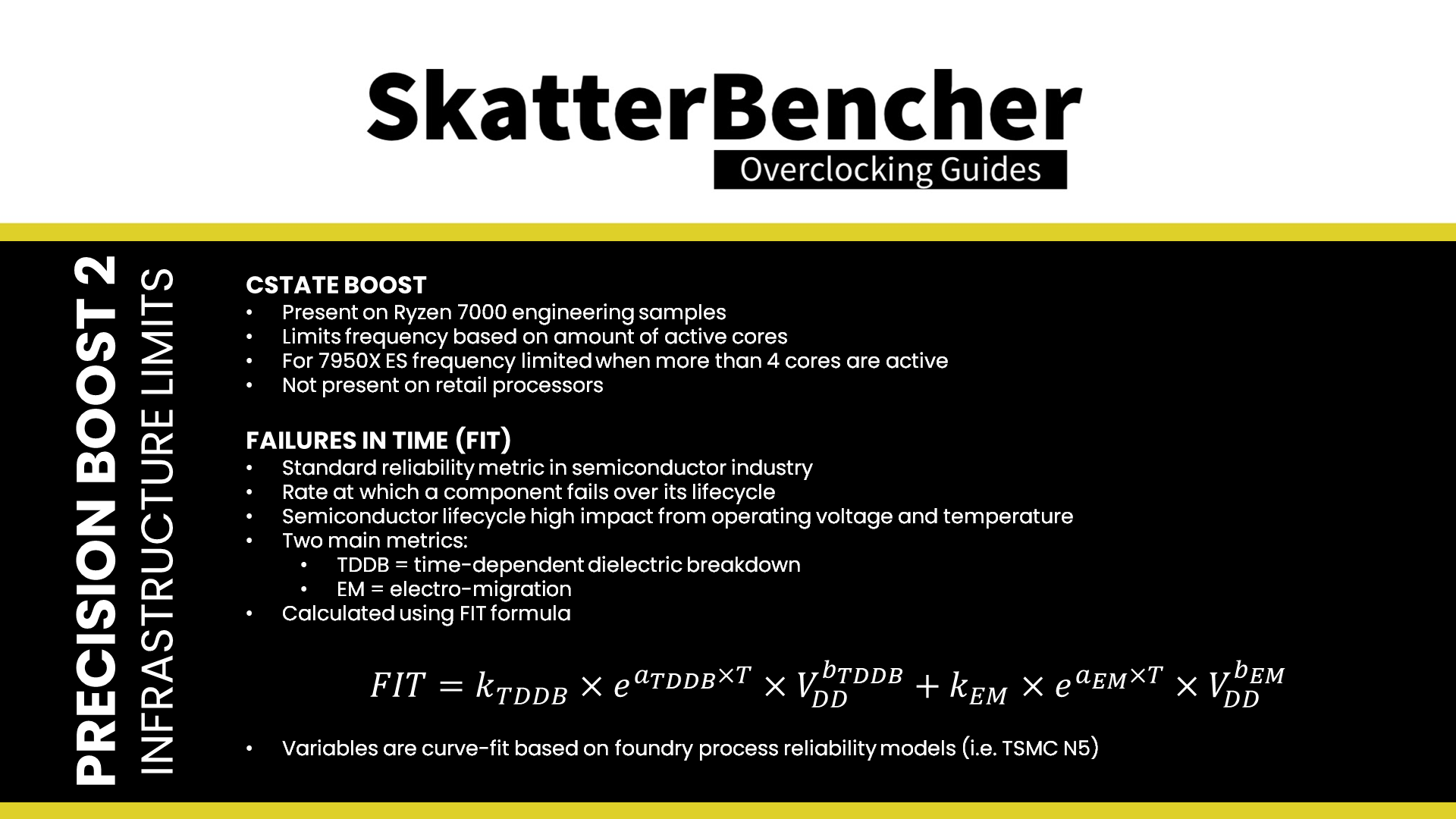
CState Boost is a specific boost limiter present on early engineering samples. Effectively, C-State Boost limits the maximum frequency when a certain number of active cores is exceeded. For the 16-core 7950X, the C-State Boost limit would force the CPU to run at 5.2 GHz when more than four cores are active. This Precision Boost limiter is not active on retail processors.
Failures in Time, or FIT, is a standard reliability engineering metric used in the semiconductor industry. It represents the rate at which a component fails over its life cycle. For semiconductors, operating voltage and temperature are the most relevant factors for failure. AMD’s real-time reliability monitoring technology incorporates two critical limiters to long-term reliability in a high-performance microprocessor: time-dependent dielectric breakdown, TDDB, and electromigration, or EM.
The FIT rate is calculated in a 1-millisecond interval using the following formula. Where the subscripted variables are curve-fit based on the foundry process reliability models. So, for Raphael, that’s based on the reliability models provided by TSMC. The calculated FIT rate then passes through a filter to ensure smoother transitions preventing the frequency from changing too quickly.In short, if the FIT rate is below the target threshold, then there’s additional frequency headroom. Suppose the FIT rate is above the target threshold. In that case, the frequency headroom is lowered to prevent any early processor failure during the product lifecycle.
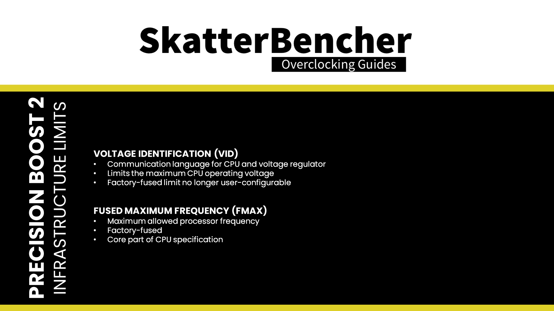
Voltage Identification, or VID, is a way for the CPU and voltage controller to communicate voltage requests. The VID limit is the maximum allowed voltage for the processor. The VID limit is factory-fused and cannot be changed by the end-user (anymore).
Fused maximum frequency, or Fmax, is the maximum allowed processor frequency. This value is fused from the factory and is obviously a core part of the CPU specification.
Adaptive Voltage Frequency Scaling
So far, I’ve talked about the Precision Boost 2 technology’s different aspects that impose limits on the maximum allowed frequency. However, we haven’t talked yet about how the maximum frequency is calculated in the first place.
Since the 2015 Carrizo APU, AMD has used Adaptive Voltage Frequency Scaling, or AVFS in short. This technology relies on Critical Path Accumulators for estimating the maximum stable frequency of circuits inside your CPU. If it sounds complicated, that’s because it is. However, I’ll try to explain it as simply as possible.

The long story short is that AMD adds replica paths to the circuit that serve no other purpose than to assess whether the circuit is stable or not. The AVFS technology extracts a Gaussian distribution statistical model from the replicate paths. It infers the stability of the “real” paths using sampling statistics. This statistical data is used by the SMU to create a Voltage-Frequency-Temperature, or VFT, table.

The VFT table is a part-specific lookup table with information on the optimal voltage for any combination of frequency and voltage. The higher the frequency and temperature, the higher the required voltage to ensure stability.


While extracting this VFT table from the CPU is impossible, I can somewhat illustrate the behavior.
In this case, I assigned a workload to a specific Zen 4 core. I tracked the VID request across different frequencies and temperatures. I configured the Precision Boost Fmax to 4600, 5000, and 5450 MHz in three scenarios

We can make three observations from the table.
First, obviously, for higher frequencies, the CPU needs higher voltages.
Two, for a given frequency, the CPU requests higher voltages as the temperature increases. For example, 4.6GHz below 40 degrees Celsius uses 1.020V, and above 90 degrees, it uses 1.068V. Similarly, 5.0GHz below 40 degrees uses 1.145V, and above 90 degrees uses 1.244V.
Third, you can see that the CPU won’t boost to the highest frequencies at high temperatures. For example, over 80 degrees Celsius, the highest frequency is 5300 MHz at 1.368V. This is the result of the Precision Boost frequency limiters we discussed before.


In 2015, this VFT table consisted of 10 rows and 8 columns, so 80 distinct data points. It’s not entirely clear if that’s still the case with the Zen 4 Ryzen 7000. Furthermore, each core inside your CPU has its own VFT table, so for a 16-core Ryzen 9 7950X, you’d have 80×16=1,280 data points.


Note that this VFT table is a factory-fused table created during manufacturing.
Boot Time Calibration
Now I hear you ask, “what if my power supply is bad?” Great question!
AMD uses automated test equipment (ATE) to fuse the VFT table onto a CPU. This test equipment typically provides a more robust, less-noisy power supply than a consumer power supply. To compensate for this, AMD uses a tester-to-platform (T2P) voltage offset. It is often a conservative over-margined value.
AMD employs a boot-time calibration (BTC) process to finetune the voltage offset. Essentially, during the boot process, the CPU can check the quality of the power delivery. Based on the quality, it then offsets the factory-fused VFT table. If you have a great power supply, the offset will be smaller. If you have a terrible power supply, then the offset will be greater.


The practical implication of boot-time calibration adjusting the voltage offset is that you can have different voltages for the same CPU depending on the power supply network. The power supply network includes the power supply, the motherboard VRM, and other electrical components between the wall socket and the CPU core.

A great power supply network would result in a smaller tester-to-platform voltage offset, thus yielding lower operating temperatures. Conversely, a poor power supply network would result in a larger boot time calibration voltage offset, thus causing higher operating temperatures.

I don’t have the time to test this in the real world, but there might be real tech media that try this out.
Boot-time calibration is an essential element of the Precision Boost technology but is disabled when switching the CPU to OC Mode.
Voltage Adaptive Operation (Clock Stretching)
Despite the advanced technologies like AVFS, the part-specific VFT table, a T2P voltage offset, and BTC, AMD cannot predict what will happen in the real world. Sometimes the voltage droop under transient conditions going from idle to load or vice versa is so significant that the system crashes.
Fortunately, AMD CPUs also have Voltage Adaptive Operation technology, more commonly known as Clock Stretching.
The technology consists of two circuits: one circuit serves as a configurable droop detector, and the second circuit functions as a configurable digital frequency synthesizer. For example, we could configure that if a voltage droop of 2.5% or more is detected, the clock period is increased by 5%.

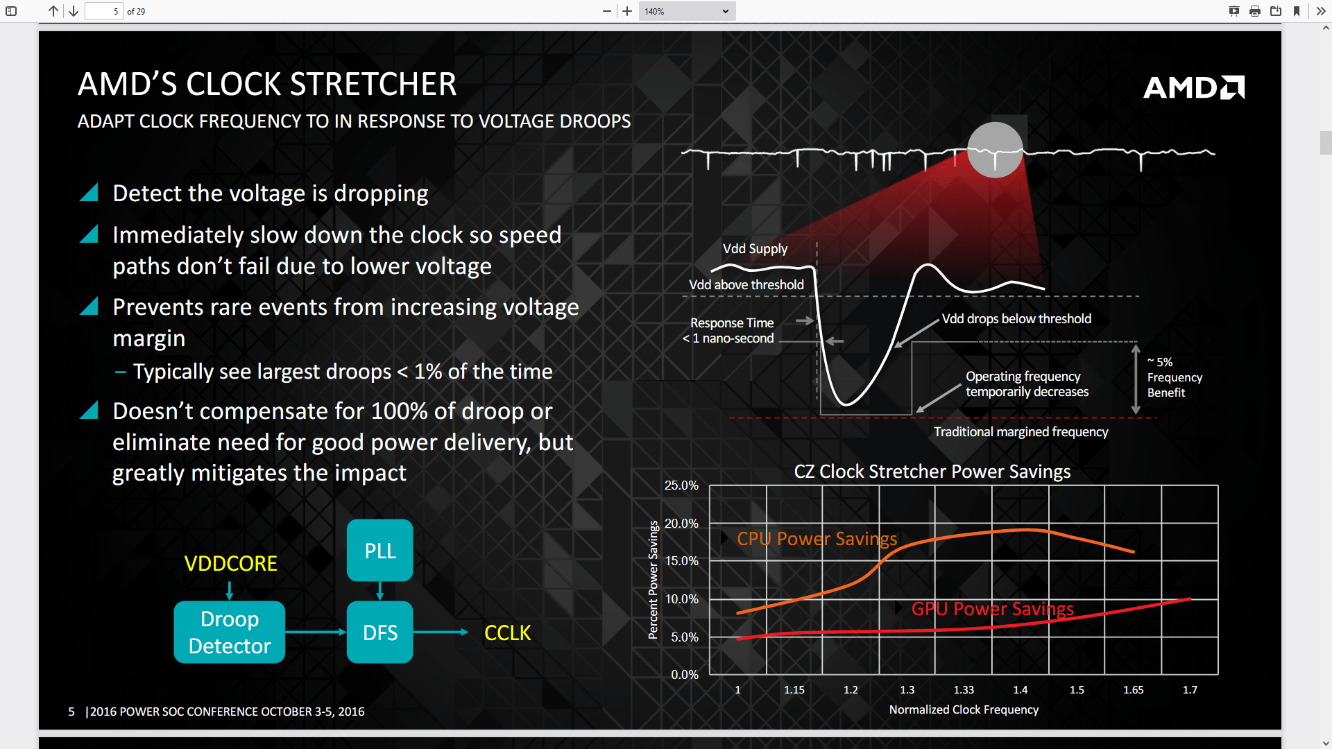
The effect is simple: if a voltage droop is detected, the effective clock frequency is lowered to ensure continuous operation instead of a system crash. In the real world, this technology is incredibly relevant when overclocking because it may cause effective performance at a given frequency to be lower than expected.
Fortunately, we can quickly check if our system is clock-stretching using tools like HWiNFO.
The practical implication of clock stretching is that the effective clock frequency will be lower than the configured core frequency.

It is essential to distinguish between these two terms.
The core frequency results from the reference clock multiplied by the CPU ratio configured by your motherboard and processor. It is a snapshot of the configured frequency at a specific moment in time. It is generally the frequency that you’ll see in tools like CPU-Z.
The effective clock frequency is the total clock cycles between two moments. It measures the actual performance of your processor within a period. You can check this value with specific tools like HWiNFO.
As illustrated in this example, the effective clock between two moments may be lower than the core frequency snapshots taken at those two moments in time. This can be due to changes in environment like workload, power-saving features when a core is idle, or clock stretching.

The best way to check if clock stretching is happening is by comparing the core frequency with the effective clock. Suppose the effective clock is significantly lower than the configured core frequency when the system is under load. In that case, clock stretching is likely happening on your system.
If you’re increasing CPU frequency but seeing stagnation or even a reduction in benchmark performance, clock stretching may be the reason.
AMD Raphael CPU Core Overclocking
Overclocking the Zen 4 Raphael CPU cores is highly similar to Zen 3 Vermeer, so it won’t be too difficult for current Ryzen users to become familiar with Raphael overclocking.
For those new to AMD Ryzen, I’ll try to quickly get you up to speed on how everything works. To keep it as simple as possible, AMD offers two routes for overclocking: Precision Boost Overdrive and OC Mode.
Precision Boost Overdrive allows you to tune some of the parameters governing the Precision Boost CPU frequency boosting algorithm. By adjusting the parameters, you can achieve better performance.
OC Mode disables the automatic frequency boosting technology and gives you manual control over some frequency and voltage parameters.
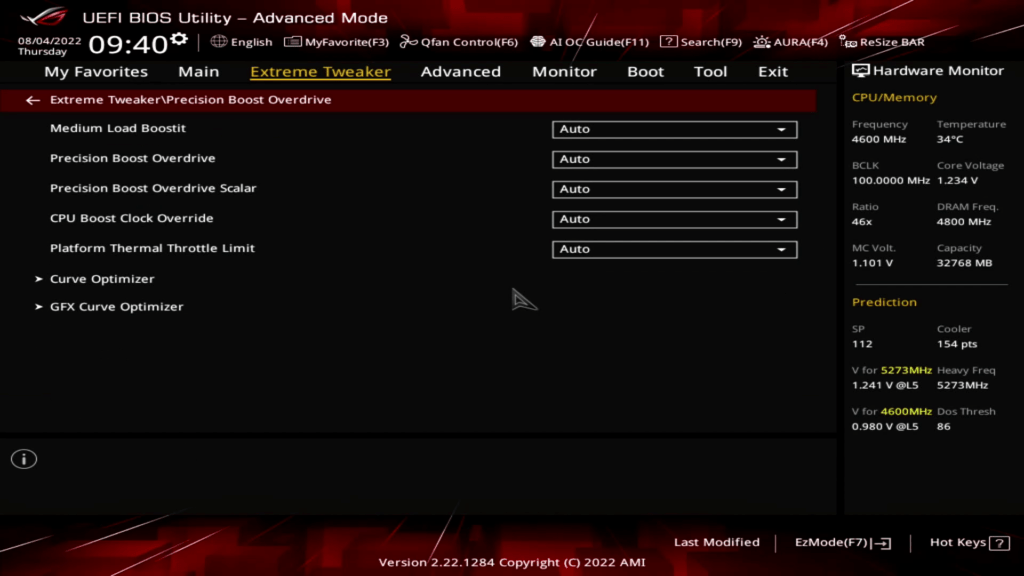
AMD Precision Boost Overdrive 2
Precision Boost Overdrive 2, or PBO 2, is AMD’s powerful overclocking toolkit that allows you to adjust some of the parameters governing the Precision Boost 2 algorithm. As a result of the tuning, you can potentially achieve higher operating frequencies for a more extended period, thus substantially improving your system’s performance.
A crucial advantage of Precision Boost Overdrive is that it retains all the intelligent frequency boosting mechanisms present in Precision Boost. That means you get both the high-frequency single-core and medium-frequency all-core boost. That sets it apart from manual overclocking, as you’ll see later in this article.

The Precision Boost Overdrive 2 toolkit for Raphael is identical to Vermeer, so anyone already familiar with the options can skip this part of the blog post. I’ll gladly reiterate how it works for those who are unaware.
There are a total of seven tools available to tune the Precision Boost 2 algorithm:
- 4x Platform Configuration Tools: PPT, EDC, TDC, Thermal Throttle
- 3x CPU Configuration Tools: Scalar, Boost Override, and Curve Optimizer.
Package Power Tracking, or PPT, is the total power the processor can draw from the socket before the boost levels off. Typically, the limiting factor is your CPU thermal solution.
Electrical Design Current, or EDC, represents the maximum peak current the voltage rail can demand under transient conditions for a short, thermally insignificant time. Independent EDC tuning is available for both the VDDCR and VDDCR_SOC voltage rails. Typically, the limiting factor is the choice of VRM components and their maximum rated specification.
Thermal Design Current, or TDC, represents the maximum sustained current the voltage regulator can support. Independent TDC tuning is available for both the VDDCR and VDDCR_SOC voltage rails. Typically, the limiting factor is the choice of VRM thermal solution and the VRM components.
Platform Thermal Throttle allows the user to decrease the maximum allowed processor temperature. The configurable values range from 0 to the product-specific TjMax, typically 95 degrees Celsius. Lowering the thermal throttling point is generally not recommended as it will negatively impact your performance. However, it can be helpful if you want to run a temperature as low as possible.

Scalar is a tool that allows the user to override the warranted silicon stress level, or FIT, to achieve higher frequency. You can adjust the maximum allowed FIT level to 10 times higher than the factory-fused limit. While the tool offers precise granularity, typically, you’ll find the available options to range between 1X and 10X in steps of 1 multiple.
The effect of increasing Scalar is that the Precision Boost algorithm should aggressively pursue higher voltages as it is less concerned with CPU lifespan.
Boost Clock Override, or Fmax Override, allows the user to override the arbitrary clock frequency limit between -1000 MHz and +200 MHz in steps of 25 MHz. It is available for both the CPU core clock and, if present, the Graphics core clock. It’s important to note that the override only adjusts the upper ceiling of the frequency and doesn’t act as a frequency offset. Ultimately, the Precision Boost 2 algorithm still determines the actual operating frequency.
On some motherboards, you may see Fmax Override options higher than +200 MHz. While it may be possible to write these values to the processor registers, they won’t actually get applied.
Curve Optimizer is a tool that allows the user to adjust the voltage margin of each individual CPU core. It does this by offsetting the voltage of the CPU core VFT table. While you don’t have exact control over the voltage of each frequency-temperature point, Curve Optimizer allows you to effectively undervolt your CPU.
Curve Optimizer allows end-users to adjust the factory-fused VFT curve, or voltage-frequency-temperature curve, for each CPU core separately. The VFT curve is a unique curve for each core inside your CPU that defines the required voltage for a given frequency at a given temperature. Higher frequencies or higher operating temperatures require higher voltage.
Curve Optimizer adjusts the VFT curve by offsetting the voltages of the factory-fused VFT curve. By setting a positive offset, you increase the voltage point. Conversely, you decrease the voltage point by setting a negative offset.
You can offset the entire curve by up to 30 steps in a positive direction and up to 300 steps in a negative direction. Each step represents around 5mV.

It may seem odd that the negative curve optimizer has expanded to 300 steps. I’ll get back to that later
The traditional overclocking approach for AMD Ryzen CPUs is to set a negative curve optimizer. Two things happen when you adjust the VFT curve with a negative point offset.
- You effectively tell the CPU that it needs less voltage for a given frequency. And, as a consequence, at a given voltage, it can apply a higher frequency. So, when the Precision Boost 2 algorithm determines sufficient power and temperature headroom to use 1.35V, with the negative point offset, it will target a higher frequency.
- The CPU temperature will be lower because you use less voltage at a given frequency. That extra thermal headroom will also encourage the Precision Boost algorithm to target higher voltages and frequencies.
Now, to get back to the negative 300 curve optimizer. This one’s a bit difficult to illustrate as BIOS options and public tools only allow up to 30 steps. However, with non-public tools, I was able to gather additional data.
The approach is straightforward: I record the actual voltage and effective clock frequency during a workload as I adjust the curve optimizer setting. I do this for three scenarios where I vary the voltage offset from the CPU Vcore voltage regulator.
As a quick reminder: the CPU will issue the voltage request to the voltage regulator with a VID request. The voltage regulator then adjusts the voltage output according to this request. When we use a negative curve offset, the VID request from the CPU is lower, and thus the voltage output from the voltage regulator is lower. We can also configure the voltage controller to add a positive offset to the VID request. Then the output voltage will be the CPU VID plus any offset from the controller.

The scenarios are: 0mV offset, +50mV offset, and +100mV offset.
First, look at the chart mapping the curve optimizer setting and the actual voltage. As you can see, adding a voltage offset to the voltage controller adjusts the impact of the negative curve optimizer on the effective voltage.

For example, at -40 curve optimizer, the actual voltage is
- 1.22V with 0mV offset,
- 1.257V with +50mV offset, and
- 1.288V with +100mV offset.

Also, 1.22V is achieved with a curve optimizer setting of
- -40 with 0mV offset,
- -52 with 50mV offset, and
- -64 with 100mV offset.

Second, let’s look at the chart mapping the voltage/frequency curve. Here we can see the impact of the curve optimizer and voltage offsets on the operating frequency. The curve is homogenous, indicating that the Precision Boost algorithm always tries to maximize the frequency for a given operating voltage regardless the curve optimizer or voltage offset.

We can see that at 1.23V, the frequency is
- 5290 MHz with a -29 curve optimizer and 0mV offset,
- 5298 MHz with a -50 curve optimizer and +50mV offset, and
- 5306 MHz with a -62 curve optimizer and +100mV offset

Further experimentation showed that up to -72 is stable with a +150mV offset. With a +750mV offset, I could test a -300 curve optimizer. Beyond -300, there was no further effect on the voltage or frequency.
In the ASUS ROG BIOS, you can access the Precision Boost Overdrive settings via the Extreme Tweaker Precision Boost Overdrive submenu. Alternatively, you can also use the Precision Boost Overdrive sub-menu settings in the AMD Overclocking menu.
OC Mode
In addition to overclocking using Precision Boost Overdrive, AMD Ryzen CPUs also offer overclockers the tools to take direct control over their CPU’s operating voltage and frequency. This is unofficially called “OC Mode.” When OC Mode is enabled, all automatic frequency boost and power-saving technologies are disabled.
One could question the use-case for manual overclocking an AMD Ryzen CPU. Just like with all past Ryzen processors, the major downside of manual overclocking is that you lose the benefits of Precision Boost technology yielding high frequency in low-threaded benchmark applications. So, whereas a 7950X can boost up to 5700 MHz with Precision Boost, it will be limited to your set fixed frequency when manually overclocking.
However, manual overclocking is not all negative and even has some benefits.
- Automatic overclocking and frequency boosting technologies leave a little margin on the table. We can exploit this margin and finetune for application- and system-specific stability when manually overclocking.
- On AMD Ryzen CPUs, you can set the frequency for each CCX separately. So, we can exploit the fact that some CCXs may overclock better than others. This is particularly relevant for the Ryzen 9 7950X and 7900X.
- By setting a fixed voltage, we avoid the CPU dynamically and rapidly updating its VID requests to the VRM controller. This alleviates stress on the VRM and typically yields lower temperatures.

The maximum frequency will depend on your desired level of stability and choice of stress-test tool.
In the ASUS ROG BIOS, you can configure a manual CPU overclock via the Extreme Tweaker CPU Core Ratio (Per CCX) submenu. Alternatively, you can manually adjust the CPU core frequency in the AMD Overclocking Manual CPU Overclocking sub-menu.

ECLK Asynchronous Mode
It is worth reminding that Raphael also supports three clock generator modes: internal clock, external clock synchronous, and external clock asynchronous. Adjusting the reference clock can also help to overclock the CPU cores, especially when using an external clock in asynchronous mode.
In asynchronous mode, there are two distinct external 100MHz reference clocks. One clock provides the 100MHz input for the CPU PLL, and another provides the 100MHz reference clock for the SOC PLLs. That means you can increase the reference clock for the CPU cores independent of your CPU’s other parts. This may come in handy when finetuning using either Precision Boost Overdrive or OC Mode.
In the ASUS ROG BIOS, you can choose the clock generator mode by setting Ai Overclock Tuner. If set to Auto, then the internal clock generator is used. If set to Manual, the external clock generator is used. You can choose synchronous or asynchronous mode for the external clock generator.

CPU Core Voltage
The CPU core voltage is provided by the VDDCR_CPU internal voltage rail, which is powered by the VDDCR external voltage rail. The internal voltage rail is bypassed; thus, the external voltage rail controls the core voltage directly.

You don’t need to adjust this voltage in regular operation with Precision Boost. However, if you want to set a manual overclock in OC Mode, you must configure the voltage directly. There are two ways to configure the voltage:
- Configure the “OCVID,” which sets the VID the CPU will request to the voltage controller
- Configure the VDDCR external voltage rail, which configures the output voltage of the voltage controller directly


In practical terms, there is no difference between the two approaches.
In the ASUS ROG BIOS, you can configure the OCVID via the Extreme Tweaker CPU Core Ratio (Per CCX) submenu. Alternatively, you can manually adjust the OCVID in the AMD Overclocking Manual CPU Overclocking sub-menu.

In the ASUS ROG BIOS, you can configure the VDDCR voltage rail directly in the Extreme Tweaker menu by adjusting the CPU Core Voltage setting.

AMD Raphael Infinity Fabric Overclocking
The Infinity Fabric, sometimes called Scalable Data Fabric, serves as the primary means of communication between all the chips on the Raphael package. Every chip on the package has a set of GMI links, short for Global Memory Interconnect, via which the CCDs communicate with the IOD.
The infinity fabric frequency and performance are most relevant for performance tuning with regards to the memory subsystem performance. Since the DDR5 memory controllers are located on the IO die, if the CPU cores need to store or retrieve data to and from the DDR5 memory, it has to go via the infinity fabric to the IO die.
Fabric Clocking
The Fabric frequency, or FCLK, is generated by the SOC PLL, derived from a 100 MHz reference clock input. The reference clock is multiplied by the FCLK ratio, which you can configure in the BIOS.

The standard operating frequency of the infinity fabric used to be 1 to 1 with the memory controller and system memory. However, that’s different on AMD Raphael. Instead, the Infinity Fabric is decoupled from the system memory and CPU memory controller frequency. By default, it runs at 1733 MHz.
It is still suggested that running the fabric clock in sync with the system memory and memory controller frequency provides the optimal performance point. Like Zen 3, a sufficiently high memory frequency can overcome any performance penalty from not running in sync. However, given the DDR5 frequency capabilities, I don’t suggest focusing too much on running everything in sync, as it’s unlikely you’ll be able to
In the ASUS ROG BIOS, you can configure the fabric frequency via the FCLK Frequency setting in the Extreme Tweaker menu. Alternatively, you can also adjust the frequency in the AMD Overclocking Infinity Fabric Frequency and Dividers sub-menu.

Fabric Voltage
The VDDG voltage supply, derived via an integrated voltage regulator from the VDDCR_MISC voltage rail, provides the fabric voltage. There are a total of four VDDG voltage rails available for manual adjustment:
- CCD0-CCD VDDG: signals sent from CCD0 to IOD are sent at this voltage
- CCD0-IOD VDDG: signals sent from IOD to CCD0 are sent at this voltage
- CCD1-CCD VDDG: signals sent from CCD1 to IOD are sent at this voltage
- CCD0-IOD VDDG: signals sent from IOD to CCD1 are sent at this voltage
Note that the VDDG voltage does not adjust automatically with VDDCR_MISC. So, if you need to increase VDDG, for example, to support higher memory frequency, you need to change it manually.

In the ASUS ROG BIOS, you can configure the VDDCR_MISC in the Extreme Tweaker menu. Alternatively, you can adjust the voltage by accessing the AMD Overclocking VDD Misc l sub-menu.

In the ASUS ROG BIOS, you can configure the VDDG voltage by accessing the AMD Overclocking VDDG Voltage Control sub-menu.

AMD Raphael Memory Controller Overclocking
AMD Raphael has two DDR5 Unified Memory Controllers, or UMC in short. Each consists of one memory channel. The memory controllers are located in the IO die. While the Zen 4 memory controller technically should support DDR4, AMD has clarified that the AM5 platform will only support DDR5 memory.
Memory Controller Clocking
The Unified Memory Controller frequency, or UCLK, is derived from the UMCCLK, one of the SOC PLLs. The UMCCLK is driven by a 100 MHz reference clock derived from either an internal or external clock generator.
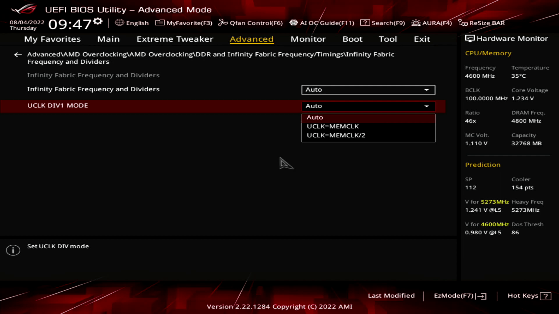
The memory controller frequency is tied directly to the system memory frequency. It can run either at the same or half its frequency. At default, the memory controller runs at the same frequency as the system memory at 2400 MHz. Still, you can theoretically increase it up to 6000 MHz when running DDR5-12000.

In the ASUS ROG BIOS, you can configure the Memory Controller frequency via the Memory Frequency setting. You can force the memory controller to run at half the memory frequency by accessing the AMD Overclocking Infinity Fabric Frequency and Dividers sub-menu and setting UCLK DIV1 Mode.
Memory Controller Voltage
The memory controller voltage is provided by the VDDCR_SOC voltage rail. You may need to increase the voltage to increase the system memory frequency. This will also increase the voltage for other IP blocks powered by the VDDCR_SOC voltage rail, such as the SMU and PSP.

In the ASUS ROG BIOS, you can configure the VDDCR_SOC voltage rail by adjusting the CPU SOC Voltage setting. Alternatively, you can change the AMD Overclocking SoC Voltage sub-menu voltage.

AMD Raphael Memory Overclocking
Raphael is AMD’s first CPU with DDR5 memory support. While it may seem like a significant technological jump from DDR4 to DDR5, the overclocking process is similar to previous AMD platforms.
There are also two new features related to memory clocking: EXPO and DDR On The Fly.
DDR5 Memory Clocking
The DDR5 memory frequency, or MCLK, is derived from the UMCCLK, one of the SOC PLLs. The UMCCLK is driven by a 100 MHz reference clock derived from either an internal or external clock generator.
Without adjusting the reference clock, you can set the memory controller frequency at 1000 MHz, 1200 MHz, or 1600 MHz, then every 100 MHz step between 1600 MHz and 6000 MHz. So all the way up to DDR5-12000.

In the ASUS ROG BIOS, you can configure the Memory frequency via the Memory Frequency setting. Alternatively, you can set the memory frequency in the AMD Overclocking DDR Timings Configuration sub-menu by adjusting the Memory Target Speed setting.

DDR5 Memory Timing Overrides
Of course, Raphael also supports overriding the DDR5 memory timings, as it’s crucial for improving memory performance. Here’s a list of supported memory timings:
DDR SPD Timing:
- Tcl: CAS latency (tAA)
- Trcd: RAS to CAS Delay Time (tRCD)
- Trp Minimum Row Precharge Delay Time (tRP)
- Tras: Minimum Active to Precharge Delay Time (tRAS)
- Trc: Minimum Active to Active/Refresh Delay Time (tRC)
- Twr: Minimum Write Recovery Time (tWR)
- Trfc1: Minimum Refresh Recovery Delay Time (tRFC1)
- Trfc2: Refresh Recovery Delay Time (tRFC2)
- TrfcSb: Refresh Recovery Delay Time (tRFCsb)
DDR non-SPD Timing
- Trtp: Read CAS# to Precharge Delay (tRTP)
- TrrdL: Activate to Activate Delay Time, same bank group (tRRD_L)
- TrrdS: Activate to Activate Delay Time, different bank group (tRRD_S)
- Tfaw: Four Activate Window Time (tFAW)
- TwtrL: Minimum Write to Read Time, same bank group (tWTR_L)
- TwtrS: Minimum Write to Read Time, different bank group (tWTR_S)
- TrdrdScL: Read to Read Delay, same chip select, same bank group
- TrdrdSc: Read to Read Delay, same chip select, different bank group
- TrdrdSd: Read to Read Delay, same DIMM
- TrdrdDd: Read to Read Delay, different DIMM
- TwrwrScL: Write to Write Delay, same chip select, same bank group
- TwrwrSc: Write to Write Delay, same chip select, different bank group
- TwrwrSd: Write to Write Delay, same DIMM
- TwrwrDd: Write to Write Delay, different DIMM
- Twrrd: Write to Read Delay
- Trdwr: Read to Write Delay

In the ASUS ROG BIOS, you can access the memory timings in the Extreme Tweaker DRAM Timing Control sub-menu. Alternatively, you can also access the memory timings in the AMD Overclocking DDR SPD Timing and DDR non-SPD Timing sub-menus.

DDR5 Memory Voltage
As we already know, there’s a significant difference between DDR4 and DDR5 regarding voltage supply to the memory. On DDR5 memory, the majority of the voltage regulation happens on the module by the PMIC. PMIC stands for Power Management Integrated Circuit.
The DDR5 PMIC has two input voltages: 5V and 3.3V. The specification further defines 4 switching output regulators for 2 times VDD, VDDQ, and VPP, and 2 LDO outputs of 1.8V and 1.0V.
- VDD is 1.1V
- VDDQ is 1.1V
- VPP is 1.8V
The PMIC also has many other features, such as I2C and I3C, over-voltage and over-temperature protection, and so on. Every DDR5 stick has its own PMIC, so you can run different voltages on the sticks. Fortunately, most motherboards will allow you to sync the voltage of your memory modules.

There’s still one memory-related voltage regulated by the CPU, the VDDP_DDR voltage. VDDP is the supply voltage for the DDR5 bus signaling and is derived from the VDDIO_MEM_S3 voltage rail. By definition, VDDP should always be 100mV lower than the VDDIO_MEM_S3 voltage.
While it is derived from the VDDIO voltage rail, VDDP does not automatically adjust with the rail. So, if you want to change the VDDP, you must manually do so via BIOS options. Of course, motherboard vendors can implement auto-rules to facilitate voltage configuration.

In the ASUS ROG BIOS, you can access the DDR5 memory voltages in the Extreme Tweaker Advanced Memory Voltages sub-menu. VDD and VDDQ are also available in the main Extreme Tweaker menu. Alternatively, you can access the DDR5 memory voltages in the AMD VDDIO Voltage Control and VPP Voltage Control sub-menus.

In the ASUS ROG BIOS, you can configure the VDDIO_MEM_S3 and VDDP_DDR voltage rails in the Extreme Tweaker sub-menu. Alternatively, you can adjust the VDDIO_MEM_S3 voltage in the AMD Overclocking VDDIO Voltage Control sub-menu under the APU VDDIO Adjust option, and the VDDP_DDR voltage in the AMD Overclocking VDDP Voltage Control sub-menu.

AMD Extended Profiles for Overclocking (EXPO)
The AMD Extended Profiles for Overclocking, or AMD EXPO, is developed to enable ubiquitous memory overclocking profiles for AMD platforms supporting DDR5 memory. Its purpose is to allow memory vendors to program higher-than-JEDEC-performance profiles onto the SPD of the memory sticks. The user can then enable these settings with a single option in the BIOS. The result is that customers can unleash their full memory performance with essentially the click of a single button.

If this sounds very familiar to you … it’s because it is.
This is not the first time AMD has ventured into high-performance memory specification. In 2012, AMD had AMD Memory Profile, or AMP, for DDR3 memory. Some of you may also remember AMD releasing their own Radeon memory sticks!


Initially, the standard was not supposed to be named EXPO but RAMP. RAMP stood for Ryzen Accelerated Memory Profile. Unfortunately, trademark issues may have prevented AMD from using that name.
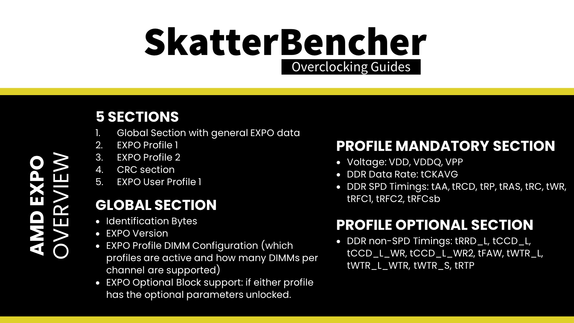
AMD EXPO has 5 main sections: one section for the general EXPO information, two sections for two EXPO profiles, a section for CRC, and a user profile section. Each EXPO profile has two sections: one with mandatory parameters and one with optional parameters.
The general EXPO section has a couple of configurable fields:
- EXPO Identification Bytes
- EXPO Version
- EXPO Profile DIMM Configuration (which profiles are active and how many DIMMs per channel are supported)
- EXPO Optional Block support: if either profile has the optional parameters unlocked.
The EXPO Profile mandatory section includes the following parameters:
- Voltage: VDD, VDDQ, VPP
- DDR Data Rate: tCKAVG
- DDR SPD Timings: tAA, tRCD, tRP, tRAS, tRC, tWR, tRFC1, tRFC2, tRFCsb
The EXPO Profile optional section includes the following parameters:
- DDR non-SPD Timings: tRRD_L, tCCD_L, tCCD_L_WR, tCCD_L_WR2, tFAW, tWTR_L, tWTR_L_WTR, tWTR_S, tRTP
At the moment of taping, it appears that AMD EXPO is a self-certification program where memory vendors can claim EXPO readiness. The EXPO specification outlines a minimum stability requirement of running memtest and 3DMark for eight hours. Additionally, a 50-cycle reboot test should be performed to ensure ACPI state transition stability.
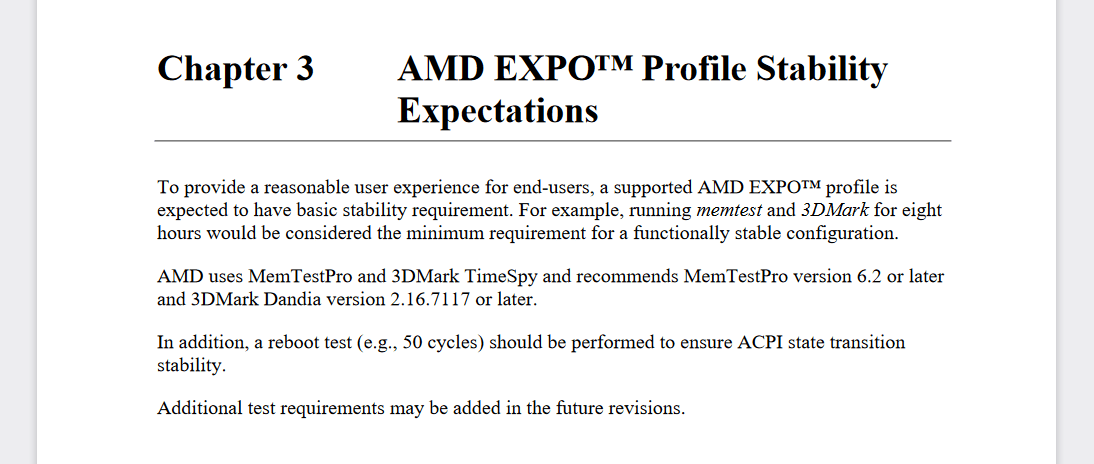
It is expected that further test and validation requirements will be added in the future.
Since the EXPO validation method is still quite rudimentary, it is expected that, initially, there will be some stability-related challenges. A lot will depend on the willingness of the motherboard and memory vendors to perform extensive compatibility and validation testing. While we should expect issues to iron out over time, be aware that you may have to accept the early adopter price when purchasing AM5 Raphael at launch.
In the ASUS ROG BIOS, you can enable EXPO in the Extreme Tweaker menu by adjusting the Ai Overclock Tuner setting. EXPO I will load only the memory primary timings, the memory frequency, and memory voltages. The rest of the profile timings is ignored and tuned by the ASUS motherboard auto-rules. EXPO II will also load the rest of the complete EXPO profile.

DDR On the Fly OC Mode
A new feature on AMD Ryzen is the ability to automatically overclock the system memory in the operating system. This feature is called “DDR On the Fly OC Mode” and is available on systems where AMD EXPO memory is installed and enabled.
DDR On The Fly OC Mode is active only when explicitly enabled. When enabled, spare DF Pstates are used to store different EXPO profiles. At boot, the CPU will train the various memory profiles. That ensures the CPU can dynamically change P-state at runtime to change the memory performance.
While DDR On The Fly OC Mode is available in the AMD BIOS, unfortunately, I could not get it to work at the time of writing. I can enable the function, but the system will not complete POST resulting in the need to clear CMOS. This function may work on another motherboard, BIOS, or with different memory.
In the ASUS ROG BIOS, you can enable DDR On The Fly OC Mode in the AMD Overclocking DDR Timing Configuration sub-menu. Navigate to the DDR and Infinity Fabric Frequency/Timings sub-menu, then DDR Options, then access the DDR Timing Configuration sub-menu. Here you can enable DDR on the fly.

Memory Context Restore
As it’s AMD’s first foray with DDR5 memory, undoubtedly, there will be memory overclocking and stability problems at launch. While memory overclocking should improve in the weeks and months following the launch, I expect early adopters to face some difficulties.
To increase the chance of a successful memory overclock, I recommend disabling a memory controller option called Memory Context Restore.
Memory Context Restore enables or disables forced DRAM re-training at every boot. Training is a DRAM process that aims to optimize the signal integrity between the CPU memory controller and DRAM memory chips. Better signal integrity means better stability at higher frequencies. Memory training can be a lengthy process. So, to improve a system’s boot-up speed, BIOS routines typically skip some parts or even the entire process.
I find that disabling this option, and thus forcing the DRAM training process on every boot, significantly improves memory stability at higher frequencies. Sadly, it also lengthens the boot-up process.
In the ASUS ROG BIOS, you can disable Memory Context Restore in the Extreme Tweaker DRAM Timing Control submenu.

AMD Raphael Integrated Graphics Overclocking
Brand new on AMD Raphael is that the desktop Ryzen CPUs now also have integrated graphics. While that would technically make it an APU, AMD still refers to it as a CPU. There are a couple of crucial differences with APUs.
First, the graphics cores are integrated into the IO die. That’s a separate chip from the CPU core dies. That’s different from APUs, where everything is integrated into a single die.

Second, the graphics on Raphael are not meant to run any kind of 3D load. It, of course, can, but it’s abysmal performance.

Since the integrated graphics are not meant for any 3D workload, overclocking the integrated graphics is currently not supported. It is unlikely to be supported in the future.
ASUS ROG Crosshair X670E Gene Overclocking Technologies
ASUS AI Overclocking Features
ASUS introduced AI Overclocking on its Z490 ROG motherboards as a next-generation automatic overclocking technology see SkatterBencher #10). Since then, it’s been present on every next Intel platform; however, not on any AMD platform. That changes with the AM5 Raphael.
ASUS AI overclocking uses a unique strategy for automatic overclocking. Instead of working with preset frequency and voltage profiles, the system monitors the CPU and cooling system throughout an initial testing phase. Based on its findings, it then predicts the optimal settings. The system automatically guides the overclocking process and adjust voltages and frequency to match your cooling system.
The better your cooling, the higher your AI overclock.

In addition to automatic overclocking, AI Overclocking provides a lot of advanced information and suggestions in the AI Features menu. The information includes:
- P0 VID and SP values for each CPU core
- Precision Boost Overdrive 2 suggested overclocking parameters
- Dynamic OC Switcher suggested overclocking parameters
The SP value is based on the combination of maximum boost frequency, temperature, and P0 VID. Generally, it indicates the quality of a particular core. A higher SP value would indicate a better-quality core with superior overclocking capabilities, though it’s not an exact science. The overclocking suggestions are based on a continued evaluation of your CPU thermal solution.

In the ASUS ROG BIOS, you can access the AI overclocking information in the Extreme Tweaker AI Features submenu.
The easiest way to get started with AI Overclocking is to first run a bunch of heavy all-core workloads in the operating system. This will help the motherboard evaluate your thermal solution. Then, go back into the BIOS and press F11. Follow the instructions and click Enable AI.

ASUS Dynamic OC Switcher
Dynamic OC Switcher, or DOS for short, is ASUS’ clever way of addressing a core challenge when overclocking AMD Ryzen processors. It was first introduced with the ASUS ROG Crosshair VIII Dark Hero motherboard (see SkatterBencher #27) and has since been included in several other ASUS motherboards.
As we know from the Raphael CPU Overclocking overview, there are two approaches to AMD Ryzen CPU core overclocking: Precision Boost Overdrive and OC mode.
- Precision Boost Overdrive has the benefit of retaining all the automatic boost algorithms, including the peak single thread frequency and associated performance.
- OC Mode enables precise per-CCX finetuning of the maximum stable all-core frequency.
So, you typically have to choose to compromise either the best single-threaded performance or the best multi-threaded performance.
ASUS Dynamic OC Switcher gives us the best of both worlds, allowing the system to actively switch between Precision Boost Overdrive and manual OC Mode at runtime. It’s most easy to conceptualize DOS as retaining all automatic Precision Boost benefits but with a manually configured frequency floor for all-core workloads.
DOS requires little additional configuration work. We need to know two things:
- What is the lowest frequency we will allow
- At which point do we want DOS to switch between PBO and OC Mode
Sadly, we cannot simply configure a minimum frequency and have the system switch based on that. Instead, we need to use a proxy metric: a specific current or temperature threshold.
In the ASUS ROG BIOS, you can access the Dynamic OC Switcher settings in the Extreme Tweaker CPU Core Ratio (Per CCX) submenu.

There is no specific method of determining the perfect threshold, so I’ll show you one example using Prime95 without AVX.
The first step is to determine your desired manual overclock. The fastest way to get to this point is by selecting your stress test tool of choice, finding the maximum CPU voltage within your thermal budget, then finding the maximum stable frequency for that voltage and temperature. In my case, I use the following settings:
- Stress Test: Prime95 non-AVX
- OCVID: 1.25V (1.12V under load)
- Loadline: Level 5 (motherboard auto-rules)
- Temperature: 90C, below TjMax of 95C
- Frequency: 5325 MHz (CCX0 = 5350 MHz, CCX1 = 5300 MHz)
We can write the settings down and switch back to tuning with Precision Boost Overdrive.
The next step is to apply all your Precision Boost Overdrive tuning settings, including any custom Curve Optimizer or Fmax Override settings. In my case, I use the following settings:
- PPT, TDC, EDC = 1000 (motherboard auto-rules)
- Fmax offset = +200
- Curve Optimizer = -15

Then go into the operating system and open your stress test tool and HWiNFO. We aim to find where the Precision Boost frequency drops below our target manual overclock of 5325 MHz and check the current use. In HWiNFO, we will monitor the CPU Core Clock and ASUS EC VRM Vcore Current.
Then we start the Prime95 non-AVX stress test and change the affinity to 1 core in task manager. Now monitor the core clock frequency. It will be higher than our target of 5325 MHz.
Now you can gradually increase the active thread count. When you reach 5325 MHz or below, check the ASUS EC VRM Vcore Current reading. This value will be our input for the DOS Current Threshold setting.
In my case, we reach the frequency of 5325 MHz at 6 active threads, and the current reads about 67A.
Now we can go back into the BIOS, add our manual overclocking settings to the already active Precision Boost Overdrive settings, and configure the Dynamic OC Switcher. In my case, I set the Current Threshold to Switch to OC Mode to 67A.
So, to reiterate what’s happening: Dynamic OC Switcher will actively switch between OC mode and Precision Boost when the CPU current hits 67A. Anything above 67A engages manual OC mode; anything below 67A will engage Precision Boost.

ASUS Voltage Suspension
Voltage Suspension is again not a new feature as it was first introduced on the Crosshair VIII Extreme motherboard (SkatterBencher #29). While it’s a relatively advanced tuning feature, I find it particularly useful for maximizing the all-core frequency when using Precision Boost Overdrive.
The term suspension is akin to a car’s suspension, though I prefer the more technical term V-Clamp. The purpose of V-Clamp is to force the Core Voltage to stay within a specific range even when using a dynamic voltage like with Precision Boost Overdrive.
To achieve that, a dedicated hardware circuitry on the motherboard PCB allows the embedded controller to read the current CPU temperature and die sense voltage. Then the controller instructs the voltage controller to adjust the voltage according to our custom suspension rules.

We can configure the Voltage Suspension by setting the voltage ceiling and floor.
Obviously, the ceiling is our maximum voltage, and the floor is our minimum voltage. We can configure the ceiling and floor in static mode or dynamic mode.
In Static mode, we set a maximum and minimum voltage. The Voltage Suspension function will try to keep the voltage between these two levels.
In Dynamic mode, we make our own voltage frequency curve, though we don’t use frequency as a parameter. Instead, we configure the ceiling and floor voltage as the function of four points defined by voltage and temperature. So, I guess it’s more like a voltage temperature curve.

It gets a little complicated in the BIOS, but here’s what it boils down to:
- Ceiling values determine the maximum upper limit of the allowed voltage
- Floor values determine the minimum lower limit of the allowed voltage
- Cold Temp sets the lower temperature target; lower typically means light workloads with few cores active
- Hot Temp sets the upper temperature target; higher typically means heavy multi-threaded workloads with all cores active
- VMin voltages are mapped against Hot Temp targets
- VMax voltages are mapped against Cold Temp targets

Maybe the best way to comprehend the feature is with an example. Let’s take the following parameters:
- Floor Low Vmin: 1.05
- Floor Hot Temp: 95
- Floor High Vmin: 1.30
- Floor Cold Temp: 50
- Ceiling Low Vmax: 1.20
- Ceiling Hot Temp: 88
- Ceiling High Vmax: 1.45
- Ceiling Cold Temp: 65
Now let’s put these parameters in our voltage temperature curve with temperature on the x-axis and voltage on the y-axis. We mark our four points on the graph, then connect the two ceiling points and the two floor points. Now we have a linearly scaling curve for our voltage as a function of the temperature.
Linear scaling means voltage suspension limits slide up and down the temperature scale. For example, suppose the temperature is 75 degrees Celsius. In that case, the voltage ceiling voltage will be about 1.35V, and the voltage floor will be 1.15V.
Note that the scaling does not continue linearly, but the ceiling and floor are the upper and lower bounds of the voltage target. So, 1.45V is the voltage ceiling at 65 degrees Celsius and below. And 1.20V is the voltage ceiling at 88 degrees Celsius and above. The same applies to the floor voltages.
Moving these four configurable points will alter the voltage temperature scaling according to your needs.

Note that Voltage Suspension is still affected by the CPU VCore load-line and doesn’t affect any undershoot or overshoot. As a reminder: voltage suspension aims to adjust the requested voltage by the CPU to stay within a pre-defined upper and lower limit. Any effect of the load-line occurs after this re-adjustment.

I found five situations where Voltage Suspension can be effective in helping you achieve higher performance when overclocking.
- Increase maximum overclocking frequency
- Increase peak effective clock
- Mitigate instability caused by aggressive Curve Optimizer settings
- Improve temperature, stability, and frequency for heavy multi-threaded workloads
- Mitigate instability caused by rapid fluctuations from heavy all-core load to idle and back
First, the obvious one: when you increase the PBO frequency using the reference clock, you will need higher voltages to ensure stability. You can use a higher ceiling voltage to have a higher voltage than Precision Boost requests. This may help you stabilize the overclock.
Second, you can achieve slightly higher peak effective clock frequencies for light workloads by trimming the maximum voltage using the voltage ceiling. The starting point would be to check the peak voltage first, then lower it step by step using the dynamic ceiling Vmax. Capping the peak voltage with our manual ceiling may trigger the CPU to sense the voltage for a given frequency is too low and increase the requested VID. That could help push the frequency slightly higher. Of course, you must check carefully for clock stretching, as trimming the voltage may cause instability.
Third, you can use Voltage Suspension to mitigate instability when running aggressive Curve Optimizer settings. As you know, Curve Optimizer allows us to manipulate the voltage frequency curve of each of our CPU cores. When using a negative curve optimizer setting, the Precision Boost algorithm will use less voltage for a given frequency. Or, of course, achieve a higher frequency for a given voltage.
However, too low voltage will result in instability. You can configure the floor Vmax so that the voltage would not drop below a certain level at light loads.
The fourth application of Voltage Suspension is the one I found most helpful. Namely mitigating the effects of using a voltage offset on heavy workload stability. An excellent illustration is when I used Voltage Suspension with the Ryzen 7 5800X3D processor in SkatterBencher #39. In my second overclocking strategy, I used reference clock and a voltage offset to achieve a higher peak frequency. This increased the voltage under load. Using Voltage Suspension, I could reduce the effective operating voltage and achieve about 200 MHz higher frequency under an all-core Prime95 workload.
Lastly, you can use Voltage Suspension to mitigate the effects of a transient load. In some situations, you may find that the workload rapidly switches between full and no load. The difference in load and its effect on the effective voltage could result in an unstable system. You can try to mitigate this issue by setting an appropriate voltage floor.
In the ASUS ROG BIOS, you can access the Voltage Suspension options in the Extreme Tweaker DIGI + VRM submenu.
ASUS Custom Algorithms
Custom Algorithms is a brand-new feature that allows you to modify the Precision Boost behavior according to your wishes. The function works like an “If This Then That” where the system monitors if a specific condition is met, then takes a specified action.
There are a total of three available algorithms. For each algorithm, you can specify a condition to monitor, two thresholds defining condition states, and 3 actions for each condition state.
There are three available conditions:
- CPU Temperature,
- Core Voltage, and
- Core Current
For each condition, you have three states: Below Level 1, between Level 1 and 2, and above Level 2. The condition measurement units are degrees Celsius for CPU Temperature, millivolts for Core Voltage, and amps for Core Current.
The system will take action based on the current state of the monitored condition.
There are eight available actions:
- Package Power Limit Fast (PPT Fast),
- Package Power Limit Slow (PPT Slow),
- Thermal Limit (THM),
- Vcore TDC Limit (CPU TDC),
- Vcore EDC Limit (CPU EDC),
- SOC TDC Limit (SOC TDC),
- SOC EDC Limit (SOC EDC), and
- ECLK ASynch BCLK
For each of the three states, we can set an action. Power is in watts, temperature is in degrees Celsius, current is in amps, and BCLK is in MHz.

Let’s give two examples.
In our first example, we want to exploit the fact that overclocking headroom is typically better at low temperatures than at high temperatures. So, we want to adjust the reference clock based on the CPU temperature. In that case, we set the following:
- Algorithm 1: Enabled
- Algorithm 1 Condition: CPU Temperature
- Algorithm 1 Action: ECLK ASynch BCLK
- Level 1 Threshold Value: 50
- Level 2 Threshold Value: 80
- Level 1 Action Value: 105
- Level 2 Action Value: 103
- Level 3 Action Value: 101
This will have the following effect:
- When the CPU temperature is below 50 degrees Celsius, the reference clock is 105 MHz
- When the CPU temperature is between 50 and 80 degrees Celsius, the reference clock is 103 MHz
- When the CPU temperature is above 80 degrees Celsius, the reference clock is 101 MHz.
That gives us a performance increase of 5%, 3%, and 1%, respectively.

In our second example, we are concerned about Precision Boost applying high voltage when the CPU temperature is very high. So, we want to adjust the thermal limit based on the CPU voltage. In that case, we set the following:
- Algorithm 1: Enabled
- Algorithm 1 Condition: Core Voltage
- Algorithm 1 Action: Thermal Limit
- Level 1 Threshold Value: 1200
- Level 2 Threshold Value: 1300
- Level 1 Action Value: 85
- Level 2 Action Value: 75
- Level 3 Action Value: 65
This will have the following effect:
- When the Core Voltage is below 1.2 volts, the thermal limit is 85 degrees Celsius
- When the Core Voltage is between 1.2 and 1.3 volt, the thermal limit is 75 degrees Celsius
- When the Core Voltage is above 1.3 volts, the thermal limit is 65 degrees Celsius

In the ASUS ROG BIOS, you can access the Custom Algorithm options in the Extreme Tweaker Custom Algorithms submenu.

ROG True Voltician
ROG True Voltician was first introduced on select ROG Z690 motherboards and is now also available on the ROG Crosshair X670E Gene and Extreme. The term Voltician is a combination of voltage and optician. As you can already guess, it’s a tool for observing the voltages of your system. On the ROG X670E boards, there are three channels for Vcore, SOC voltage, and CPU current.
The Voltician is a USB oscilloscope. You can use it on your system directly or connect it via USB to a second system. The two options require a slightly different setup.
If you want to use the Voltician to check the voltage on your system, simply plug the device into an available USB header on the motherboard. Then connect the 3 channel inputs to the OSC Sense pin headers on the motherboard.
You’ll need to use the micro-USB cable if you want to connect the Voltician to a separate system. Then, you need to connect the Voltician Ground pin to any ground on the motherboard. For example, using one of the FAN headers.
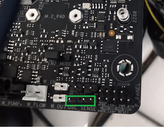


Remote monitoring has 2 main benefits:
- You can continue to monitor the voltage even if the target system shuts down
- The monitoring speed is not affected by the system load
By default, the Voltician has a voltage range from 0 to 3.3V. However, using different pin configurations, you can also enable 0 to 5V or 0 to 12V range.
You can use the ROG True Voltician Dashboard application to monitor the voltage. The dashboard has two main functions: Oscilloscope System and Data Analysis.


You can monitor the three channels at run time in the Oscilloscope system. There are several options to finetune your view so you can set it up as you please.
In the Data Analysis, you can record the voltage data, export it to a CSV file, then analyze the data afterward.
One example of how you can use the Voltician is to analyze the behavior of the CPU VRM loadline. In my example, I’ve set the CPU ratio to 45X, the CPU voltage to 1.15V, and I’m using Prime95 Small FFTs without AVX on all cores. As you can see, the difference between LLC1 and LLC8 is substantial, with LLC1 having an average voltage of 0.933V and LLC8 having an average voltage of 1.116V. Choosing the right loadline can mean the difference between stability and instability under heavy workloads.

AMD Raphael Overclocking Expectations
We can split the overclocking expectations into ambient cooling and extreme cooling.
For ambient overclocking, I expect the following maximum overclocking results when using a 16-core Raphael CPU with high-end custom loop water cooling.
- 6.0 GHz at 1.50V for 1-core maximum frequency
- 5.9 GHz at 1.45V for 1-core gaming stable frequency
- 5.5 GHz at 1.30V for 8-core gaming stable frequency
- 5.4 GHz at 1.25V for all-core gaming stable frequency
- 5.2 GHz at 1.15V for all-core maximum stable frequency
- 5.1 GHz at 1.05V for all-core AVX-512 maximum stable frequency
- 2.133 GHz for FCLK maximum stable frequency
- 3.2 GHz for UCLK maximum stable frequency
- DDR5-6400 for maximum stable memory frequency
- VDDCR_SOC = VDD = VDDQ = 1.4V
- 175 MHz for the reference clock frequency
This is almost the overclock I managed during one of my early recorded test sessions.

So, compared to Ryzen 5000 Zen 3 Vermeer:
- 700 MHz more for the single-core frequency range
- 700 MHz more for the single-CCX frequency range
- 600 MHz more for the dual-CCX frequency range
- 700 MHz more for the dual-CCX AVX frequency range
- Similar overclocking capability for the fabric frequency
- 1000 MHz for the memory controller frequency
- 1200 MHz more for memory frequency
These overclocking margins are also in line with what we can see for extreme overclocking.
AMD Raphael Overclocking Example
Now that we have learned all there is to know about AM5 and Raphael overclocking, we can move on to the practical part. I will first review the overclocking concept and then show a practical example.
Overclocking Concept
Raphael offers an incredible range of overclocking strategies and opportunities. Ryzen overclockers are already familiar with the main avenues of Precision Boost Overdrive and OC Mode. Now there’s a third route in the form of Asynchronous Eclk.
- Use Precision Boost Overdrive platform configuration tools like PPT, TDC, and EDC, which will allow for higher frequencies to be maintained for longer
- Use Precision Boost Overdrive processor configuration tools like Fmax, Scalar, and Curve Optimizer.
- Fmax increases the frequency ceiling, allowing for higher frequencies in lighter loads
- Scalar lowers the reliability concern, allowing for the use of higher voltages
- Curve Optimizer offsets the voltage-frequency-temperature table, forcing lower voltages at a given frequency-temperature point, thus enabling boosting to higher frequencies at a given voltage
- Use OC Mode, which allows us to manually finetune the CPU to work at a specific voltage-frequency point regardless of the temperature
- Use Asynchronous Eclk with Precision Boost, which increases the frequency at a specific voltage-temperature point

The trade-off between Precision Boost Overdrive and OC Mode is well-known to Ryzen overclockers. While OC Mode generally allows for a more finetuned and higher all-core overclock, you give up the high-frequency boost in lighter fewer-core workloads. With Ryzen 7000’s higher frequencies, the difference between all-core and single-core maximum frequency can be 500 MHz or more.

Asynchronous Eclk throws a curve ball to the traditional approach of using Precision Boost Overdrive as it’s the antithesis to Curve Optimizer. Whereas Curve Optimizer will lower the voltage for a given frequency-temperature point, Eclk will increase the frequency for a given voltage-temperature point. Logically, tuning one knob will affect the tuning range of the other.
This makes it more difficult to find an optimal tuning process. I spent some time trying to find the best approach to tuning a Ryzen 7000 CPU. I will detail the process so you can try it out for yourself as well and, if you want to, share your findings in the comments below.
Overclocking Process: Baseline
First, let’s establish the goal.
The goal of our tuning is to increase the maximum frequency, average frequency, and minimum frequency across all cores, workload types, and thread count. I use a tool by Shamino, which measures the average core frequency across all active cores in a fixed workload from 1 to 31 active threads.
Our baseline configuration is with Precision Boost Overdrive enabled (unleashes PPT, EDC, TDC) and 100 MHz Eclk.
Please note that I’m using an engineering sample CPU, so the boost frequencies don’t match the retail CPUs. That said, the general tuning process still applies to retail CPUs.
The baseline frequency is characterized by this line and ranges from 5398 MHz at 1 active thread to 5100 MHz with 31 active threads. The programmed Fmax is 5450 MHz, meaning the base configuration effective Fmax is 99% of the programmed Fmax. This will be important later on. The average frequency is 5200 MHz, and the minimum frequency is 5100 MHz.

Then, I try three variations of the Precision Boost Overdrive processor configuration tools:
- Curve Optimizer all cores with -30 negative offset
- The above, but with an added Fmax offset of +200 MHz
- The above, but with an adjusted Scalar of 10X.
The Curve Optimized frequency ranges from 5450 MHz at 1 active thread to 5293 MHz with 31 active threads. The programmed Fmax is 5450 MHz, meaning the base configuration effective Fmax is 100% of the programmed Fmax. This is why I add the +200MHz Fmax in the next variation. The average frequency is 5365 MHz (+165MHz over base) and the minimum frequency is 5293 MHz (+193MHz over base).
The Fmax adjusted frequency ranges from 5526 MHz at 1 active thread to 5304 MHz with 31 active threads. The programmed Fmax is 5650 MHz which means our effective Fmax is at 97.8%. The average frequency is 5366 MHz (+1MHz over CO) and the minimum frequency is 5304 MHz (+9MHz over CO).
Unfortunately, the scalar adjustment made no difference in maximum, average, or minimum frequency.

In the next step, I tried exploring the overclocking headroom provided by the asynchronous eclk. For each of the three variations (base, curve optimizer, and fmax), I tried to find the maximum stable Eclk.
The base case, that’s 106 MHz, for the Curve Optimized case is 102.25 MHz, and the Fmax Offset case is 102.25 MHz. The base case with maximum Eclk provides both the highest maximum frequency and average frequency. It is matched by the Fmax Offset case in minimum frequency.
The base case with Eclk frequency ranges from 5684 MHz at 1 active thread to 5436 MHz with 31 active threads. The programmed Fmax is 5777 MHz which means our effective Fmax is 98.4%. The average frequency is 5495 MHz (+295 MHz over base), and the minimum frequency is 5421 MHz (+321 MHz over base).

Then, further finetuning can begin. The next step is to find the sweet spot between Eclk and Curve Optimizer. I increase the all-core Curve Optimizer in steps of negative five and adjust the Eclk to ensure stability. I find that the sweet spot is negative 10 CO with an Eclk of 104.75 MHz.
The sweet spot case frequency ranges from 5688 MHz at 1 active thread to 5430 MHz with 31 active threads. The programmed Fmax is 5736 MHz which means our effective Fmax is at 99.2%. The average frequency is 5500 MHz (+300 MHz over base), and the minimum frequency is 5430 MHz (+330 MHz over base).

Overclocking Process: Finetuning
The initial overclocking process has provided a good baseline, but there’s still much work left. We’ll tackle maximizing frequency while retaining stability in various applications in the finetuning part of the overclocking process.
The frequency will be maximized by finetuning the Curve Optimizer settings on a per-core basis. This will exploit the fact that some cores can overclock better than others.
Ensuring stability will require us to run a more extensive set of benchmarks and stress test applications than the one we’ve used in our baseline tuning process. The benchmark applications range from the lightest single-threaded workload to the most demanding all-core workload. There is no definitive set of workloads to stress-test, so you are free to define stability according to your own interpretation.
In my case, the lightest workload is NOP Bench, and the most challenging workload is 30 minutes of Prime 95 small FFTs with AVX enabled. There’s a set of benchmarks I regularly use that fit between those two extremes: Geekbench 5, Cinebench R23, CS:GO, 3DMark, AI Benchmark, etc. My typical requirement for a stable overclock is that my system must be able to run all these workloads consecutively.

A quick word on NOP Bench. This is a small application written by Elmor from Elmorlabs. It essentially loads the CPU cores by running a NOP instruction. NOP is a one-byte instruction that means no operation. So, effectively we’re asking the CPU to do nothing as fast as possible. In my opinion, the overclocking community may consider this a better frequency validation standard.
Next, a word on Prime95. I had some difficulties getting AVX512 to run on the latest Prime95 version. So, this time, I will ignore my requirements and use Prime95 Small FFTs without AVX as a worst-case stress test.
After a couple more hours of finetuning, we can go into the BIOS and configure what I think could be a typical high-performance overclock with a Ryzen 9 7950X Engineering Sample and EK-Quantum custom loop water cooling.
Overclocking Process: Example
Upon entering the BIOS
- Go to the Extreme Tweaker menu
- Set Ai Overclock Tuner to EXPO I
- Set eCLK Mode to Asynchronous mode
- Set BCLK2 Frequency to 104
- Set FCLK Frequency to 2000 MHz
- Enter the Precision Boost Overdrive sub-menu
- Set Medium Load Boostit to Enabled
- Set Precision Boost Overdrive to Enabled
- Set CPU Boost Clock Override to Enabled (Positive)
- Set Max CPU Boost Clock Override(+) to 200
- Enter the Curve Optimizer sub-menu
- Set Curve Optimizer to Per Core
- Set Core 0 Curve Optimizer Sign to Negative
- Set Core 0 Curve Optimizer Magnitude to 20
- Set Core 1 Curve Optimizer Sign to Negative
- Set Core 1 Curve Optimizer Magnitude to 20
- Set Core 2 Curve Optimizer Sign to Negative
- Set Core 2 Curve Optimizer Magnitude to 20
- Set Core 3 Curve Optimizer Sign to Negative
- Set Core 3 Curve Optimizer Magnitude to 5
- Set Core 4 Curve Optimizer Sign to Negative
- Set Core 4 Curve Optimizer Magnitude to 15
- Set Core 5 Curve Optimizer Sign to Negative
- Set Core 5 Curve Optimizer Magnitude to 15
- Set Core 6 Curve Optimizer Sign to Negative
- Set Core 6 Curve Optimizer Magnitude to 20
- Set Core 7 Curve Optimizer Sign to Negative
- Set Core 7 Curve Optimizer Magnitude to 10
- Set Core 8 Curve Optimizer Sign to Negative
- Set Core 8 Curve Optimizer Magnitude to 5
- Set Core 9 Curve Optimizer Sign to Negative
- Set Core 9 Curve Optimizer Magnitude to 10
- Set Core 10 Curve Optimizer Sign to Negative
- Set Core 10 Curve Optimizer Magnitude to 20
- Set Core 11 Curve Optimizer Sign to Negative
- Set Core 11 Curve Optimizer Magnitude to 20
- Set Core 12 Curve Optimizer Sign to Negative
- Set Core 12 Curve Optimizer Magnitude to 5
- Set Core 13 Curve Optimizer Sign to Negative
- Set Core 13 Curve Optimizer Magnitude to 20
- Set Core 14 Curve Optimizer Sign to Negative
- Set Core 14 Curve Optimizer Magnitude to 10
- Set Core 15 Curve Optimizer Sign to Negative
- Set Core 15 Curve Optimizer Magnitude to 0
- Leave the Curve Optimizer sub-menu
- Leave the Precision Boost Overdrive sub-menu
Then save and exit the BIOS.
This was just a first look at Ryzen 7000 overclocking. I will provide more detailed overclocking information in future SkatterBencher overclocking guides.
When running Prime 95 Small FFTs with AVX disabled at stock, the average CPU effective clock is 4821 MHz with 1.1 volts. The average CPU temperature is 82.3 degrees Celsius, and the average CPU package power is 207.8 watts. The Precision Boost algorithm is limited by the CPU TDC, which is maxed out at 160A.

When running Prime 95 Small FFTs with AVX disabled overclocked, the average CPU effective clock is 5146 MHz with 1.129 volts. The average CPU temperature is 95.2 degrees Celsius, and the average CPU package power is 260.5 watts. The Precision Boost algorithm is limited by the maximum allowed CPU temperature.

Conclusion
Alright, that’s it for this article.
As you can see, there’s much to talk about regarding AM5 and Raphael overclocking. This is the most exciting AMD platform for overclocking in a very long time, and I expect enthusiasts to thoroughly enjoy tuning their system.
In the coming weeks, I’ll put out some SkatterBencher overclocking guides for Raphael CPUs. So, stay tuned for that.
I’d like to thank my Patreon supporters for supporting my work.
As usual, if you have any questions or comments, feel free to drop them in the comment section below.
See you next time!
Animag771
How did you get past the -30 CO limit?
I’ve been experimenting with low wattage tuning on my 5700X. I have limited it to 49W PPT and when under such tight power limits it appears that the lower I can get the voltage, the higher my all-core frequency is able to go. I’m currently using -30 CO all-cores and an additional -72mV VCore offset. Without the negative Vcore offset it only gets 2.6GHz all-core but with the negative offset I’m able to hit 3.4GHz (effective) and 4.947GHz single-core (102 BCLK). The problem is, more negative VCore offset will lower the voltage too far and it won’t be able to maintain the high single-core frequency.
It seems like the best option would be to further reduce Curve Optimizer and get rid of some of that negative VCore offset.
PS: Yes it clock stretches under all-core loads but if I tune for no clock stretching the real performance is much lower.
SkatterBencher #76: AMD Ryzen 7 8700F Overclocked to 5250 MHz - SkatterBencher
[…] most recently took a deep dive into the Precision Boost Overdrive 2 toolkit in my Ryzen 7000 launch content. If you want to learn more about the impact of each of these settings, I suggest you check out that […]
SkatterBencher #72: AMD Ryzen 5 8600G Overclocked to 5250 MHz - SkatterBencher
[…] most recently took a deep dive into the Precision Boost Overdrive 2 toolkit in my Ryzen 7000 launch content. If you want to learn more about the impact of each of these settings, I suggest you check out that […]
SkatterBencher #71: AMD Ryzen Threadripper 7960X Overclocked to 5715 MHz - SkatterBencher
[…] most recently took a deep dive into the Precision Boost Overdrive 2 toolkit in my Ryzen 7000 launch content. If you want to learn more about the impact of each of these settings, I suggest you check out that […]
SkatterBencher #69: AMD Ryzen 7 8700G Overclocked to 5350 MHz - SkatterBencher
[…] most recently took a deep dive into the Precision Boost Overdrive 2 toolkit in my Ryzen 7000 launch content. If you want to learn more about the impact of each of these settings, I suggest you check out that […]
9 New Things About Overclocking Ryzen Threadripper 7000 - SkatterBencher
[…] counterparts. In fact, it is so similar to Ryzen 7000 overclocking that I suggest you check out my Raphael launch content for more details on how AMD Ryzen 7000 overclocking […]
SkatterBencher #60: AMD Ryzen 7 7800X3D Overclocked to 5400 MHz - SkatterBencher
[…] explored the ins and outs of Precision Boost Overdrive 2 tuning in my AMD Raphael Overclocking launch article. If you want to learn more about the impact of each of these settings, I suggest you check out that […]
ScomComputersHello Peter
Hi Peter!
Since I have been following you and watching your videos for a very long time, I have a question! What do you think is the maximum safe voltage for Ryzen 7000 processors for fixed vcore and fixed clock speed 24/7 ? Igors Lab here defines it as 1.300-1.450V , depending on the processor !
Please tell me what your opinion is !
https://www.igorslab.de/en/ryzen-7000-tuning-guide-infinity-fabric-expo-dual-rank-samsung-and-hynix-ddr5-in-practice-test-with-benchmarks-recommendations/10/
Pieter
In my experience, liquid-cooled dual-CCD Zen 4 hits 95~100C at 1.15-1.25V in all-core workloads. So naturally that would be my limit. For single-CCD, probably 100mV higher would be fine.
That’s of course my suggestion for “daily” systems, not what’s the maximum “safe” limit.
ScomComputers
Thank you for your reply!
So you’re saying that for a 7600X and a 7700X with allcore OC 24/7 1.350V is safe?
I read many places that they would not go above 1.2V,then this is fake news right ?
Thanks for your help !
Pieter
I don’t know the context of why it was said above 1.20V isn’t safe, so I cannot say it’s fake news or not.
For the 7600X and 7700X, you can look at my SkatterBencher guide. In particular, look at the voltage in OC Strategies where I rely on PBO. You’ll find that AMD’s own Precision Boost algorithm boosts to 1.35-1.38V under Prime95 all-core load. My perspective is that if it’s safe enough for AMD’s Precision Boost (which comes with a 3Y warranty), it’s probably safe enough for a manual overclock.
MJ
I’m using 7950x3d and I’m trying to overclock memory and I found this post while searching for vdd misc voltage. I read it with concentration using a translator. Thank you for the good information
Update on Ryzen 7000 C-State Boost Limiter - SkatterBencher
[…] I want to shed more light on the Precision Boost C-State Boost limiter I discussed previously in my Raphael launch blog. Here is what I had to say about this […]
Let's Talk 6 GHz Raptor Lake - SkatterBencher
[…] overclocking guides, plus Arc A380, in August. Obviously, that did not work out. Not only because Raphael’s testing took up all of the available time with new AGESAs and so many different tuning tactics to uncover. […]
SkatterBencher #48: AMD Ryzen 5 7600X Overclocked to 5544 MHz - SkatterBencher
[…] explored the ins and outs of Precision Boost Overdrive 2 tuning in my AMD Raphael Overclocking launch article. If you want to learn more about the impact of each of these settings, I suggest you check out that […]
SkatterBencher #46: AMD Ryzen 9 7900X Overclocked to 5900 MHz - SkatterBencher
[…] explored the ins and outs of Precision Boost Overdrive 2 tuning in my AMD Raphael Overclocking launch article. If you want to learn more about the impact of each of these settings, I suggest you check out that […]
SkatterBencher #45: AMD Ryzen 9 7950X Overclocked to 5950 MHz - SkatterBencher
[…] my AMD Raphael overclocking launch article, I explored the ins and outs of Curve Optimizing with Precision Boost Overdrive 2. If you want to […]
SkatterBencher #47: AMD Ryzen 7 7700X Overclocked to 5750 MHz - SkatterBencher
[…] explored the ins and outs of Precision Boost Overdrive 2 tuning in my AMD Raphael Overclocking launch article. If you want to learn more about the impact of each of these settings, I suggest you check out that […]